EP0107290A2 - Nichtflüchtige Halbleiterspeicheranordnung mit Funktionen für elektrische Wahl, Löschung und Programmierung - Google Patents
Nichtflüchtige Halbleiterspeicheranordnung mit Funktionen für elektrische Wahl, Löschung und Programmierung Download PDFInfo
- Publication number
- EP0107290A2 EP0107290A2 EP83304916A EP83304916A EP0107290A2 EP 0107290 A2 EP0107290 A2 EP 0107290A2 EP 83304916 A EP83304916 A EP 83304916A EP 83304916 A EP83304916 A EP 83304916A EP 0107290 A2 EP0107290 A2 EP 0107290A2
- Authority
- EP
- European Patent Office
- Prior art keywords
- inverter
- timing signal
- program
- delay
- mos transistor
- Prior art date
- Legal status (The legal status is an assumption and is not a legal conclusion. Google has not performed a legal analysis and makes no representation as to the accuracy of the status listed.)
- Granted
Links
Images


Classifications
-
- G—PHYSICS
- G11—INFORMATION STORAGE
- G11C—STATIC STORES
- G11C16/00—Erasable programmable read-only memories
- G11C16/02—Erasable programmable read-only memories electrically programmable
- G11C16/06—Auxiliary circuits, e.g. for writing into memory
- G11C16/34—Determination of programming status, e.g. threshold voltage, overprogramming or underprogramming, retention
- G11C16/3418—Disturbance prevention or evaluation; Refreshing of disturbed memory data
- G11C16/3427—Circuits or methods to prevent or reduce disturbance of the state of a memory cell when neighbouring cells are read or written
-
- G—PHYSICS
- G11—INFORMATION STORAGE
- G11C—STATIC STORES
- G11C16/00—Erasable programmable read-only memories
- G11C16/02—Erasable programmable read-only memories electrically programmable
- G11C16/06—Auxiliary circuits, e.g. for writing into memory
- G11C16/32—Timing circuits
-
- G—PHYSICS
- G11—INFORMATION STORAGE
- G11C—STATIC STORES
- G11C16/00—Erasable programmable read-only memories
- G11C16/02—Erasable programmable read-only memories electrically programmable
- G11C16/06—Auxiliary circuits, e.g. for writing into memory
- G11C16/34—Determination of programming status, e.g. threshold voltage, overprogramming or underprogramming, retention
- G11C16/3418—Disturbance prevention or evaluation; Refreshing of disturbed memory data
Definitions
- This invention relates to a nonvolatile semiconductor memory device which is electrically selectable, erasable and programmable.
- MOS FET type memory cell with a floating gate and a control gate, as shown in Fig. 1.
- data is electrically selectable, erasable and programmable.
- Each memory cell has a source S and a drain D which are formed on the semiconductor substrate, a floating gate FG formed on a channel region between the source S and the drain D, first and second control gates CG1 and CG2 capacitance-coupled with the floating gate FG, and a program electrode EG for programming the data at the floating gate.
- the program electrode EG opposes the floating gate FG with a very thin insulating film interposed therebetween to allow a tunnel current to flow.
- FIG. 2 A matrix array of the memory cells of this type, i.e., 4-bit memory, is shown in Fig. 2.
- Memory cells Ml - M4 are so connected that the drains and the first control gates in the same column are interconnected, respectively, the second control gates in the same row are interconnected, and the sources S and the electrodes EG of all the memory cells are interconnected.
- the memory device is of the N-channel MOS FET type.
- the drain Dl and the second control gate CG21 are set at high potential, while the remaining electrodes are set at low potential.
- the memory cell Ml is logical "1”
- a channel current flows into the memory cell Ml.
- no channel current flows into this memory cell.
- the memory cell Ml is in the logical "1" state when no charge is written in the floating gate FG; it is in the logical "0” state when electrons are injected in the floating gate FG and the threshold voltage Vtl is high and positive.
- the first and second gates CG11 and CG21 are set at high potential, while the remaining terminals are set at low potential.
- the potential at the floating gate FG is sufficiently higher than that at the program electrode EG.
- the first and second control gates CG11 and CG21 are set at low potential, while the remaining terminals are set at high potential to erase the contents of the memory cell M1.
- the potential at the gate FG is sufficiently lower than that at the electrode EG. Therefore, a tunnel current flows between the floating gate FG and the program electrode EG, thus programming the memory cell Ml.
- the potentials at the first and second control gates CGl and CG2 and the program electrode EG concurrently change at the program start time point to.
- the nonvolatile semiconductor memory device is electrically selectable, erasable and programmable.
- the memory device involves the following problems.
- the potentials at the electrodes and gates of the memory cells are externally controlled, and some time delay is inevitable in transferring signals for such potential control. Therefore, it is difficult to obtain the ideal and simultaneous potential changes as shown in Fig. 3.
- the first and second control gates CG1 and CG2 are at high potential and the program electrode EG is at low potential.
- the first and second control gates CG1 and CG2 are at low potential and the program electrode EG is at high potential. In either case, undesirable change of the contents of the memory cells may occur.
- the object of the present invention is to provide a nonvolatile semiconductor memory device which can be electrically selectable, erasable and programmable and in which the contents of the memory cells other than the selected do not change.
- the nonvolatile semiconductor memory device electrically selectable, erasable and programmable functions, which comprises a plurality of memory cells arranged in rows and columns, each of the memory cells including a source and a drain separately formed on the semiconductor substrate, a floating gate formed on an insulating film formed on a channel region between the source and drain, a program electorde opposing the floating gate with a very thin insulation film interposed therebetween, and first and second control gates formed in a capacitance-coupled manner on an insulation film formed on the floating gate, the first control gates of the memory cells of each column being connected to one another and the second control gates of the memory cells of each row being connected to one another; select circuit for properly selecting memory cell by setting a potential relation between the first and second control gates; and .timing circuit for providing a program inhibition period ranging over a period including a time point at which a program potential for programming the contents in the memory cell selected by the select circuit is supplied to the program electrode, the timing means keeping one of
- the nonvolatile semiconductor memory device is reliable.
- FIGs. 4 to 7 show a nonvolatile semiconductor memory device according to the present invention.
- a source 2 and a drain 3, both being of N + type, are fabricated in the surface region of a P type silicon substrate 1.
- a gate insulation layer 4a is formed on a channel region located between the source 2 and the drain 3.
- a floating gate 5 is formed on this gate insulation layer 4a.
- a first control gate 6 and a second control gate 7 are formed above the floating gate 5 in a capacitance-coupled manner.
- a gate insulating film 4b is interposed between the gate 5 and the first control gate 6, and a gate insulating film 4c is interposed between the gate 5 and the second control gate 7.
- N + layer 8 i.e., a program electrode formed integrally with the source 2 is located adjacent to the channel region.
- the floating gate 5 extends over the N + layer 8 and opposes the N + layer 8 with a very thin insulating film 4d interposed therebetween.
- the first control gate 6, i.e., a program control electrode extends in the column direction of a memory matrix.
- the second control gate 7 used for the program control and for a read gate and the floating gate 5 cover the channel region.
- the gate 7 extends in the row direction of the memory matrix.
- the source 2 continuously extends in the row direction, while the drains 3 are connected by a metal interconnection wire extending in the column direction.
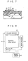
- a nonvolatile semiconductor memory device using the matrix memory array 11 described above is schematically illustrated in Fig. 8.
- a column decoder 12 is used to control the potential on the first control gate 6; a row decoder 13 to control the potential on the second control gate 7; a write/erase (W/E) control circuit 14 to apply a high potential of 20 V, for example, or a low potential of 0 V, for example, to all N + layer 8 of each memory cell.
- a timing circuit 15 is provided to control the potentials on the column decoder 12, row decoder 13 and W/E control circuit 14.
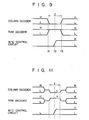
- Fig. 9 The operation of the nonvolatile semiconductor memory device in a program mode will be described, referring to Fig. 9.
- time t2 (corresponding to to in Fig. 3) data is to be programmed.
- program inhibit period T Before and after the program point t2 is program inhibit period T, from time tl to time t3, which extends over time t2.
- all outputs of the column decoder 12 are set at low potential, while all outputs of the row decoder 13 are set at high potential.
- the first control gate 6 and the second control gate 7 are set at low potential and high potential, respectively.
- the W/E control circuit 14 supplies a program control signal of high potential to the N + layer 8 in all memory cells.
- the control gates 6 and 7 are not at high or low potential. Therefore, the data of the memory cell is not changed.
- the column decoder 12 and the row decoder 13 produce the outputs for selecting a desired memory cell, to thereby program that memory cell.
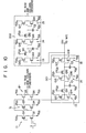
- the actual structure of the timing circuit 15 is illustrated in Fig. 10.
- a timing signal S from this circuit 15 is applied to the row and column decoders, through inverters Il and I2 connected in series and through a buffer Bl.
- the inverter Il is composed of a depletion mode MOS transistor Ql and an enhancement mode MOS transistor Q2.
- the source-drain paths of these transistors Ql and Q2 are connected to each other in series.
- the gate of the MOS transistor Ql is connected to the source of the MOS transistor Q1.
- the inverter I2 is comprised of a depletion mode MOS transistor Q3 and an enhancement mode MOS transistor Q4.
- the source-drain paths of these transistors Q3 and Q4 are series-connected.
- the gate of the MOS transistor Q3 is connected to the source of the MOS transistor.
- the buffer Bl is comprised of enhancement mode MOS transistors Q5 and Q6 whose source-drain paths are series-connected to each other.
- the gate of the MOS transistor Q5 is supplied with the output of the inverter Il, and the gate of the MOS transistor Q6 with the output of the inverter I2.
- a timing signal Sl is produced from the node of the source-drain paths of the MOS transistors Q5 and Q6, and is applied to the row and column decoders. In response to the timing signal Sl, all outputs of the column decoder 12 are set at low potential, while all outputs of the row decoder 13 are set at high potential.
- the output signal of the inverter I2 is supplied to a first delay circuit DC1, which produces a first delay timing signal DS1 with a fixed time delay.
- the signal DS1 is applied to the W/E control circuit 14, which applies a high potential, for example, + 20 V, to the N + layers 8 of all memory cells.
- the first delay circuit DC1 is comprised of inverters 13 to 15, depletion mode MOS transistors Qll and Q12, and capacitors Cl and C2.
- the inverter I3 is supplied with the output of the inverter 12.
- the output terminal of the inverter I3 is connected to the input terminal of the inverter I4 through the source-drain path of the MOS transistor Qll.
- the gate of the MOS transistor Qll is connected to a power source V DD .
- the output terminal of the inverter I4 is connected to the input terminal of the inverter I5 through the source-drain path of the MOS transistor Q12.
- the gate of the MOS transistor Q12 is connected to the power source V DD .
- the input terminals of the inverters I4 and I5 are connected to a reference voltage source V SS via the capacitors Cl and C2, respectively.
- the inverter I3 is comprised of a depletion mode MOS transistor Q13 and an enhancement mode MOS transistor Q14.
- the inverter I4 is composed of a depletion mode MOS transistor Q15 and an enhancement mode MOS transistor Q16.
- the inverter I5 is comprised of a depletion mode MOS transistor Q17 and an enhancement mode MOS transistor Q18.
- the first delay timing signal DS1 is applied to the W/E control circuit 14, delayed a given time behind the timing signal Sl.
- the first delay timing signal DS1 is also supplied to a second delay circuit DC2, which produces a second delay timing signal DS2 further delayed a predetermined time.
- the signal DS2 is applied to the row and column decoders 12 and 13, which then produce output signals to select a desired memory cell. In response to these signals, the memory cell is selected and programmed.
- the second delay circuit DC2 is identical with the first delay circuit DC1 in structure. Like symbols are used to designate like or the same elements as these of the circuit DC1.
- the potential on the first and second control gates and the program electrode are nonconcurrently changed in programming the memory cell in the memory array.
- the program inhibit period is provided for all the memory cells. In this period, one of the first and second control gates is at high potential while the other is at low potential. At the midpoint of the program inhibit period the programming potential is set. Therefore, only a desired memory cell is programmed without adversely affecting the remaining memory cells.
Landscapes
- Read Only Memory (AREA)
- Semiconductor Memories (AREA)
- Non-Volatile Memory (AREA)
Applications Claiming Priority (2)
| Application Number | Priority Date | Filing Date | Title |
|---|---|---|---|
| JP171381/82 | 1982-09-30 | ||
| JP57171381A JPS5960797A (ja) | 1982-09-30 | 1982-09-30 | 不揮発性半導体メモリ装置 |
Publications (3)
| Publication Number | Publication Date |
|---|---|
| EP0107290A2 true EP0107290A2 (de) | 1984-05-02 |
| EP0107290A3 EP0107290A3 (en) | 1987-01-14 |
| EP0107290B1 EP0107290B1 (de) | 1989-12-20 |
Family
ID=15922119
Family Applications (1)
| Application Number | Title | Priority Date | Filing Date |
|---|---|---|---|
| EP83304916A Expired EP0107290B1 (de) | 1982-09-30 | 1983-08-25 | Nichtflüchtige Halbleiterspeicheranordnung mit Funktionen für elektrische Wahl, Löschung und Programmierung |
Country Status (4)
| Country | Link |
|---|---|
| US (1) | US4571705A (de) |
| EP (1) | EP0107290B1 (de) |
| JP (1) | JPS5960797A (de) |
| DE (1) | DE3380998D1 (de) |
Families Citing this family (8)
| Publication number | Priority date | Publication date | Assignee | Title |
|---|---|---|---|---|
| GB2138230B (en) * | 1983-04-12 | 1986-12-03 | Sony Corp | Dynamic random access memory arrangements |
| US4780750A (en) * | 1986-01-03 | 1988-10-25 | Sierra Semiconductor Corporation | Electrically alterable non-volatile memory device |
| USRE37308E1 (en) * | 1986-12-22 | 2001-08-07 | Stmicroelectronics S.R.L. | EEPROM memory cell with a single level of polysilicon programmable and erasable bit by bit |
| IT1199828B (it) * | 1986-12-22 | 1989-01-05 | Sgs Microelettronica Spa | Cella di memoria eeprom a singolo livello di polisilicio scrivibile e cancellabile bit a bit |
| JPH0810728B2 (ja) * | 1990-02-01 | 1996-01-31 | 株式会社東芝 | 半導体記憶装置 |
| US5097449A (en) * | 1990-03-15 | 1992-03-17 | Vlsi Technology, Inc. | Non-volatile memory structure |
| US5818082A (en) * | 1996-03-04 | 1998-10-06 | Advanced Micro Devices, Inc. | E2 PROM device having erase gate in oxide isolation region in shallow trench and method of manufacture thereof |
| US6788614B2 (en) * | 2001-06-14 | 2004-09-07 | Micron Technology, Inc. | Semiconductor memory with wordline timing |
Family Cites Families (10)
| Publication number | Priority date | Publication date | Assignee | Title |
|---|---|---|---|---|
| US3728695A (en) * | 1971-10-06 | 1973-04-17 | Intel Corp | Random-access floating gate mos memory array |
| US4110842A (en) * | 1976-11-15 | 1978-08-29 | Advanced Micro Devices, Inc. | Random access memory with memory status for improved access and cycle times |
| JPS594790B2 (ja) * | 1978-05-18 | 1984-01-31 | 株式会社東芝 | メモリ−回路 |
| US4314265A (en) * | 1979-01-24 | 1982-02-02 | Xicor, Inc. | Dense nonvolatile electrically-alterable memory devices with four layer electrodes |
| US4393481A (en) * | 1979-08-31 | 1983-07-12 | Xicor, Inc. | Nonvolatile static random access memory system |
| US4344154A (en) * | 1980-02-04 | 1982-08-10 | Texas Instruments Incorporated | Programming sequence for electrically programmable memory |
| US4334292A (en) * | 1980-05-27 | 1982-06-08 | International Business Machines Corp. | Low voltage electrically erasable programmable read only memory |
| US4377857A (en) * | 1980-11-18 | 1983-03-22 | Fairchild Camera & Instrument | Electrically erasable programmable read-only memory |
| JPS57141969A (en) * | 1981-02-27 | 1982-09-02 | Toshiba Corp | Nonvolatile semiconductor memory |
| US4398269A (en) * | 1981-07-23 | 1983-08-09 | Sperry Corporation | MNOS Over-write protection circuitry |
-
1982
- 1982-09-30 JP JP57171381A patent/JPS5960797A/ja active Pending
-
1983
- 1983-08-25 EP EP83304916A patent/EP0107290B1/de not_active Expired
- 1983-08-25 DE DE8383304916T patent/DE3380998D1/de not_active Expired - Lifetime
- 1983-08-29 US US06/527,483 patent/US4571705A/en not_active Expired - Fee Related
Also Published As
| Publication number | Publication date |
|---|---|
| EP0107290B1 (de) | 1989-12-20 |
| US4571705A (en) | 1986-02-18 |
| DE3380998D1 (de) | 1990-01-25 |
| EP0107290A3 (en) | 1987-01-14 |
| JPS5960797A (ja) | 1984-04-06 |
Similar Documents
| Publication | Publication Date | Title |
|---|---|---|
| US4377857A (en) | Electrically erasable programmable read-only memory | |
| US4233526A (en) | Semiconductor memory device having multi-gate transistors | |
| JP2710521B2 (ja) | 反転層を含む半導体メモリ・セルおよびメモリ・アレイ | |
| US4175290A (en) | Integrated semiconductor memory array having improved logic latch circuitry | |
| US4380804A (en) | Earom cell matrix and logic arrays with common memory gate | |
| KR910019060A (ko) | 불휘발성 반도체 기억장치 | |
| EP0083194A2 (de) | Programmierbare und elektrisch löschbare Festwertspeicherzelle mit einem einzigen Transistor | |
| US4527259A (en) | Semiconductor device having insulated gate type non-volatile semiconductor memory elements | |
| US6288941B1 (en) | Electrically erasable semiconductor non-volatile memory device having memory cell array divided into memory blocks | |
| US4142251A (en) | Field programmable read-only-memory | |
| US4630087A (en) | Nonvolatile semiconductor memory device | |
| JPH0146949B2 (de) | ||
| EP1067557B1 (de) | Flashkompatibler EEPROM Speicher | |
| US4571705A (en) | Nonvolatile semiconductor memory device with electrically selectable, erasable and programmable function | |
| US5812453A (en) | Programmable semiconductor memory | |
| US4805150A (en) | Programmable semiconductor memory device having grouped high voltage supply circuits for writing data | |
| US3858060A (en) | Integrated driver circuit | |
| US5487034A (en) | Semiconductor memory device and method for writing data therein | |
| EP0317323A2 (de) | Programmierbarer Halbleiterspeicher | |
| US4636984A (en) | Semiconductor device having non-volatile storage transistors | |
| EP0508552B1 (de) | Programmierbarer Halbleiterspeicher | |
| JP2732070B2 (ja) | 不揮発性半導体記憶装置の書込み方法 | |
| US5245566A (en) | Programmable semiconductor | |
| EP0365721B1 (de) | Programmierbarer Halbleiterspeicher | |
| US20040156236A1 (en) | Programmable semiconductor memory |
Legal Events
| Date | Code | Title | Description |
|---|---|---|---|
| PUAI | Public reference made under article 153(3) epc to a published international application that has entered the european phase |
Free format text: ORIGINAL CODE: 0009012 |
|
| 17P | Request for examination filed |
Effective date: 19830908 |
|
| AK | Designated contracting states |
Designated state(s): DE FR GB IT NL |
|
| RAP1 | Party data changed (applicant data changed or rights of an application transferred) |
Owner name: KABUSHIKI KAISHA TOSHIBA |
|
| PUAL | Search report despatched |
Free format text: ORIGINAL CODE: 0009013 |
|
| AK | Designated contracting states |
Kind code of ref document: A3 Designated state(s): DE FR GB IT NL |
|
| 17Q | First examination report despatched |
Effective date: 19880224 |
|
| GRAA | (expected) grant |
Free format text: ORIGINAL CODE: 0009210 |
|
| AK | Designated contracting states |
Kind code of ref document: B1 Designated state(s): DE FR GB IT NL |
|
| PG25 | Lapsed in a contracting state [announced via postgrant information from national office to epo] |
Ref country code: NL Effective date: 19891220 Ref country code: IT Free format text: LAPSE BECAUSE OF FAILURE TO SUBMIT A TRANSLATION OF THE DESCRIPTION OR TO PAY THE FEE WITHIN THE PRESCRIBED TIME-LIMIT;WARNING: LAPSES OF ITALIAN PATENTS WITH EFFECTIVE DATE BEFORE 2007 MAY HAVE OCCURRED AT ANY TIME BEFORE 2007. THE CORRECT EFFECTIVE DATE MAY BE DIFFERENT FROM THE ONE RECORDED. Effective date: 19891220 |
|
| REF | Corresponds to: |
Ref document number: 3380998 Country of ref document: DE Date of ref document: 19900125 |
|
| ET | Fr: translation filed | ||
| NLV1 | Nl: lapsed or annulled due to failure to fulfill the requirements of art. 29p and 29m of the patents act | ||
| PLBE | No opposition filed within time limit |
Free format text: ORIGINAL CODE: 0009261 |
|
| STAA | Information on the status of an ep patent application or granted ep patent |
Free format text: STATUS: NO OPPOSITION FILED WITHIN TIME LIMIT |
|
| 26N | No opposition filed | ||
| PGFP | Annual fee paid to national office [announced via postgrant information from national office to epo] |
Ref country code: FR Payment date: 19930805 Year of fee payment: 11 |
|
| PGFP | Annual fee paid to national office [announced via postgrant information from national office to epo] |
Ref country code: GB Payment date: 19930817 Year of fee payment: 11 |
|
| PGFP | Annual fee paid to national office [announced via postgrant information from national office to epo] |
Ref country code: DE Payment date: 19930823 Year of fee payment: 11 |
|
| PG25 | Lapsed in a contracting state [announced via postgrant information from national office to epo] |
Ref country code: GB Effective date: 19940825 |
|
| GBPC | Gb: european patent ceased through non-payment of renewal fee |
Effective date: 19940825 |
|
| PG25 | Lapsed in a contracting state [announced via postgrant information from national office to epo] |
Ref country code: FR Effective date: 19950428 |
|
| PG25 | Lapsed in a contracting state [announced via postgrant information from national office to epo] |
Ref country code: DE Effective date: 19950503 |
|
| REG | Reference to a national code |
Ref country code: FR Ref legal event code: ST |