EP0099708B1 - Magnetic apparatus for reducing substrate warpage - Google Patents
Magnetic apparatus for reducing substrate warpage Download PDFInfo
- Publication number
- EP0099708B1 EP0099708B1 EP83303993A EP83303993A EP0099708B1 EP 0099708 B1 EP0099708 B1 EP 0099708B1 EP 83303993 A EP83303993 A EP 83303993A EP 83303993 A EP83303993 A EP 83303993A EP 0099708 B1 EP0099708 B1 EP 0099708B1
- Authority
- EP
- European Patent Office
- Prior art keywords
- web
- magnets
- substrate material
- travel
- deposition
- Prior art date
- Legal status (The legal status is an assumption and is not a legal conclusion. Google has not performed a legal analysis and makes no representation as to the accuracy of the status listed.)
- Expired
Links
Images

Classifications
-
- H10P72/3204—
-
- C—CHEMISTRY; METALLURGY
- C23—COATING METALLIC MATERIAL; COATING MATERIAL WITH METALLIC MATERIAL; CHEMICAL SURFACE TREATMENT; DIFFUSION TREATMENT OF METALLIC MATERIAL; COATING BY VACUUM EVAPORATION, BY SPUTTERING, BY ION IMPLANTATION OR BY CHEMICAL VAPOUR DEPOSITION, IN GENERAL; INHIBITING CORROSION OF METALLIC MATERIAL OR INCRUSTATION IN GENERAL
- C23C—COATING METALLIC MATERIAL; COATING MATERIAL WITH METALLIC MATERIAL; SURFACE TREATMENT OF METALLIC MATERIAL BY DIFFUSION INTO THE SURFACE, BY CHEMICAL CONVERSION OR SUBSTITUTION; COATING BY VACUUM EVAPORATION, BY SPUTTERING, BY ION IMPLANTATION OR BY CHEMICAL VAPOUR DEPOSITION, IN GENERAL
- C23C16/00—Chemical coating by decomposition of gaseous compounds, without leaving reaction products of surface material in the coating, i.e. chemical vapour deposition [CVD] processes
- C23C16/44—Chemical coating by decomposition of gaseous compounds, without leaving reaction products of surface material in the coating, i.e. chemical vapour deposition [CVD] processes characterised by the method of coating
- C23C16/54—Apparatus specially adapted for continuous coating
- C23C16/545—Apparatus specially adapted for continuous coating for coating elongated substrates
-
- H—ELECTRICITY
- H01—ELECTRIC ELEMENTS
- H01J—ELECTRIC DISCHARGE TUBES OR DISCHARGE LAMPS
- H01J37/00—Discharge tubes with provision for introducing objects or material to be exposed to the discharge, e.g. for the purpose of examination or processing thereof
- H01J37/32—Gas-filled discharge tubes
- H01J37/32431—Constructional details of the reactor
- H01J37/32733—Means for moving the material to be treated
- H01J37/32752—Means for moving the material to be treated for moving the material across the discharge
- H01J37/32761—Continuous moving
- H01J37/3277—Continuous moving of continuous material
-
- H—ELECTRICITY
- H01—ELECTRIC ELEMENTS
- H01J—ELECTRIC DISCHARGE TUBES OR DISCHARGE LAMPS
- H01J37/00—Discharge tubes with provision for introducing objects or material to be exposed to the discharge, e.g. for the purpose of examination or processing thereof
- H01J37/32—Gas-filled discharge tubes
- H01J37/34—Gas-filled discharge tubes operating with cathodic sputtering
-
- H10P72/3314—
Definitions
- This invention relates generally to apparatus for producing improved photovoltaic devices and more particularly to apparatus adapted to substantially reduce warping of a magnetic web of substrate material so as to produce more efficient large area photovoltaic cells.
- the present invention relates to apparatus for substantially reducing warpage of relatively large area, relatively thin webs of substrate material onto which amorphous silicon alloy layers are deposited by continuous glow discharge production techniques performed within dedicated deposition chambers. More particularly, in the continuous production glow discharge deposition apparatus of the prior art, the web of substrate material is moved, under tension, from a supply core through a plurality of deposition chambers wherein successive amorphous alloy layers are deposited. While moving through the plurality of -deposition chambers and onto a take-up core, the web of substrate material assumes a normal, elongated path of travel.
- the apparatus of the present invention is adapted to establish a plurality of substantially equally spaced magnetic fields within each of the plurality of deposition chambers for urging the web of substrate material out of its normal, sagging elongated path of travel through the plurality of deposition chambers and into a substantially planar path oftravel. In this manner, the web of substrate material is "flattened” so as to provide a substantially planar deposition surface onto which uniform amorphous alloy layers may be deposited. The result is the production of improved, more efficient large area photovoltaic devices.
- phosphine gas (PH 3 ) for n-type conduction, or diborane (B 2 H 6 ) gas, for p-type conduction is premixed with the silane gas and passed through the glow discharge reaction tube under the same operating conditions.
- the material so deposited includes supposedly sulistitutional phosphorus or boron dopants and is shown to be extrinsic and of n or p conduction type.
- the hydrogen in the silane was found to combine, at an optimum temperature, with many of the dangling bonds of the silicon during the glow discharge deposition to reduce the density of the localized states in the energy gap, thereby causing the amorphous material to more nearly approximate the corresponding crystalline material.
- Activated fluorine readily diffuses into, and bonds to, amorphous silicon in a matrix body to substantially decrease the density of localized defect states therein. This is because the small size of the fluorine atoms enables them to be readily introduced into an amorphous silicon matrix.
- Fluorine is considered to be a more efficient compensating or altering element than hydrogen when employed alone or with hydrogen, because of its exceedingly small size, high reactivity, specificity in chemical bonding, and high electronegativity.
- Compensation may be achieved with fluorine, alone or in combination with hydrogen, upon the addition of such element(s) in very small quantities (e.g., fractions of one atomic percent).
- the amounts of fluorine and hydrogen most desirably used are much greater than such small percentages, permitting the elements to form a silicon-hydrogen-fluorine alloy.
- alloying amounts of fluorine and hydrogen may, for example, be used in a range of 0.1 to 5 percent or greater.
- the alloy thus formed has a lower density of defect states in the energy gap than can be achieved by the mere neutralization of dangling bonds and similar defect states.
- fluorine participates substantially in effecting a new structural configuration of an amorphous silicon-containing material and facilitates the addition of other alloying materials, such as germanium.
- Fluorine in addition to the aforementioned characteristics, is an organizer of local structure in the silicon-containing alloy through inductive and ionic effects. Fluorine, also influences the bonding of hydrogen by acting to decrease the density of the defect states which hydrogen normally contributes. The ionic role that fluorine plays in such an alloy is an important factor in terms of the nearest neighbor relationships.
- the multiple cell structures therein discussed utilized p-n junction crystalline semi- conductor devices. Essentially the concept is directed to utilizing different band gap devices to more efficiently collect various portions of the solar spectrum and to increase open circuit voltage (Voc).
- the tandem cell device has two or more cells with the light directed serially through each cell, with a large band gap material followed by a smaller band gap material to absorb the light passed through the first cell or layer. By substantially matching the generated currents from each cell, the overall open circuit voltage is increased without substantially decreasing the short circuit current.
- the cascade cell is hereinafter referred to as a multiple cell without a separation or insulating layer therebetween.
- Each of the cells was made of an Si-H material of the same band gap in a p-i-n junction configuration. Matching of the short circuit current (J sc ) was attempted by increasing the thickness of the cells in the serial light path. As expected, the overall open circuit voltage (Voc) of the device increased and was proportional to the number of cells utilized.
- band gap adjusting element(s) such as germanium and carbon, can be activated and are added in vapor deposition, sputtering or glow discharge processes.
- the band gap is adjusted as required for specific device applications by introducing the necessary amounts of one or more of the adjusting elements into the deposited alloy cells in at least the photocurrent generation region thereof.
- the cell alloy maintains high electronic qualities and photoconductivity when the adjusting element(s) are added to tailor the device wavelength characteristics for a specific photoresponse application.
- the addition of hydrogen, either with fluorine or after deposition, can further enhance the fluorine compensated or altered alloy.
- the post deposition incorporation of hydrogen is advantageous when it is desired to utilize the higher deposition substrate temperatures allowed by fluorine.
- amorphous silicon alloys can be deposited in multiple layers over relatively large area substrates to form solar cells in a high volume, continuous processing system.
- Continuous processing systems of this kind are disclosed, for example, in EP-A-0041773 for A Method of Making P-Doped Silicon Films and Devices Made Therefrom and for a Continuous Amorphous Solar Cell Production System; EP-A-0060651 for Continuous Systems For Depositing Amorphous Semiconductor Material; and EP-A-0076426 for Multiple Chamber Deposition and Isolation System and Method.
- a web of substrate material may be continuously advanced through a succession of deposition chambers, wherein each chamber is dedicated to the glow discharge deposition of a specific amorphous semiconductor alloy material.
- the first chamber is dedicated for depositing a p-type amorphous silicon alloy layer onto the substrater
- the second chamber is dedicated for depositing an intrinsic amorphous silicon alloy layer atop the p-type layer
- the third chamber is dedicated for depositing an n-type amorphous silicon alloy layer atop the intrinsic layer.
- each one of the alloy layers be of substantially uniform thickness.
- the deposition apparatus of the prior art is unable to prevent (1) transverse warping (warping may synonymously be termed buckling or canoeing) of the web of substrate material caused by the force of gravity acting on the substrate, the elongated path of travel which the substrate follows, stresses on the web itself, the high deposition temperatures to which the substrate is continuously subjected; or (2) longitudinal warping of the web of substrate material which occurs when the tension on the substrate initiated by drive and tensioning motors is not very carefully adjusted.
- peaks and valleys are formed. It is common to have greater thicknesses of amorphous alloy materials deposited in the valleys while none or lesser thicknesses of amorphous alloy materials are deposited at the peaks.
- Such nonuniform deposition of the amorphous semiconductor alloy layers is undesirable, can create short circuits and generally serves to impair efficiency and operation of the large area photovoltaic devices produced therefrom.
- a plurality of paired punch rollers acts as an edge guide and web-tensioner for the advancing substrate.
- One method of increasing the efficiency of photovoltaic cells produced on relatively large area, relatively thin, elongated webs of substrate material is to eliminate or substantially reduce transverse and longitudinal warpage of webs of substrate material travelling through the deposition chambers. It is to this end that the apparatus of the present invention is directed.
- an apparatus for producing improved photovoltaic devices by substantially reducing warpage of a relatively large area, relatively thin, elongate web of electrically conductive, magnetically attractable substrate material following an elongate path of travel through at least one isolated deposition chamber wherein an amorphous semiconductor alloy layer is deposited onto one surface of the substrate is characterised in that a plurality of spaced magnets are disposed within the at least one deposition chamber across substantially the full width of the web of substrate material to attract and urge the web out of its normal path of travel and into a flattened, substantially planar, path of travel through the at least one deposition chamber, such that warpage of the web of substrate material is substantially reduced so that a uniform amorphous semiconductor alloy layer may be deposited onto the one surface of the web.
- the magnets are arranged in a plurality of spaced rows of magnets, each row extending transversely with respect to the path of travel of the web.
- the magnets of each spaced row may be encapsulated by means comprising, for example, a plurality of tubes for receiving the magnets.
- the encapsulated rows of magnets are preferably equally spaced at substantially 20 to 25 cm intervals.
- the magnets may be rotatably mounted whereby the web is urged into rolling contact therewith so as to reduce frictional forces therebetween.
- each row of magnets may be mounted on an axle rotatably fixed within the at least one deposition chamber.
- the unlayered surface of the magnetic web of substrate material is urged into rolling contact with the magnetic element so as not only to increase the tension and produce a flat deposition surface on the web of substrate material, but also to reduce frictional contact between the unlayered surface of the magnetic web of substrate material and the magnetic elements.
- the reduction of surface friction becomes increasingly important as the length of the path of travel of the substrate through the deposition chambers increases.
- the web of substrate material assumes a very lengthy path of travel. Since it is undesirable to provide drive motors of great power to overcome the stationary magnetic forces acting on the web, the rotatably magnetic elements become increasingly important.
- the magnetic eJements are rotatably supported within each one of the deposition chambers so as to extend substantially across the entire transverse width of the magnetic web of substrate material.
- the magnetic elements may either be a plurality of ceramic magnets having a circular periphery rotatably mounted on an axle and encapsulated by a hollow tube, or may be an electromagnetic coil rotatably disposed about an axle and encap- tulated by a tube.
- the preferred embodiment contemplates the establishment of magnetic fields about every 20 to 25 cm (eight to ten inches) along the longitudinal extent of the deposition chambers so as to reduce warpage by flattening the magnetic web of substrate material.
- a tandem or cascade-type photovoltaic cell formed of successive p-i-n layers each including an amorphous semi-conductor alloy, is shown generally by the numberal 10. It is for the mass production of this type of photovoltaic device, wherein amorphous alloy layers are continuously deposited onto a moving web of substrate material in successive isolated triads of deposition chambers that the apparatus of the present invention for substantially reducing warpage of the web of substrate material was developed.
- Figure 1 shows a plurality of p-i-n type photovoltaic devices such as solar cells 12a, 12b and 12c.
- a substrate 11 which may be transparent or formed from a metallic surfaced foil.
- the term "substrate” shall include not only a flexible film, but also any elements added thereto by preliminary processing.
- the substrate material 11 may be stainless steel, aluminum, tantalum, molybdenum or chrome.
- Each of the cells 12a, 12b and 12c are fabricated with an amorphous alloy body containing at least a silicon alloy.
- Each of the alloy bodies includes an n-type conductivity region or layer 20a, 20b and 20c; an intrinsic region or layer 18a, 18b and 18c; and a p-type conductivity region or layer 16a, 16b and 16c.
- cell 12b is an intermediate cell and, as indicated in Figure 1, additional intermediate cells may be stacked atop the illustrated cells without departing from the spirit or scope of the present invention.
- tandem p-i-n cells are illustrated, the substrate warpage reduction apparatus of this invention is utilized equally well in (1) multiple chamber apparatus which is adapted to produce tandem n-i-p cells or in (2) multiple chamber apparatus which is adapted to produce Schottky or MIS cells.
- the present invention may be utilized with any apparatus wherein warpage of large area substrates is a problem.
- the p-type layers are characterized by light absorptive, high conductivity alloy layers.
- the intrinsic alloy layers are characterized by an adjusted wavelength threshold for solar photoresponse, high light absorption, low dark conductivity and high photoconductivity, including sufficient amounts of a band gap adjusting element or elements to optimize the band gap for the particular cell application.
- the intrinsic layers are band gap adjusted to provide cell 12a with the smallest band gap, cell 12c with the largest band gap, and cell 12b with a band gap between the other two.
- the n-type layers are characterized by low light absorption, high conductivity alloy layers.
- the thickness of the n-type layers can be in the range of about 2.5 to 10 nm (25 to 100 angstroms).
- the thickness of the band gap adjusted, amorphous intrinsic alloy layers can be between about 200 to 300 nm (2,000 to 3,000 angstroms).
- the thickness of p-type layers can be between 5 to 20 nm (50 to 200 angstroms). Due to the shorter diffusion length of the holes, the p-type layers generally will be as thin as possible. Further the outermost layer, here the n-type layer 20c, will be as thin as possible to avoid absorption of light and need not include the band gap adjusting element.
- a further deposition step may be performed in a separate environment.
- a TCO (transparent conductive oxide) layer 22 is added, which layer may, for example, be indium tin oxide (ITO), cadmium stannate (Cd 2 Sn0 4 ), or doped tin oxide (Sn0 2 ).
- ITO indium tin oxide
- Cd 2 Sn0 4 cadmium stannate
- Sn0 2 doped tin oxide
- an electrode grid 24 may be added to the device, for a tandem cell having a sufficiently small area the TCO layer 22 is generally sufficiently conductive so the grid 24 is not necessary. If the tandem cell is of a sufficiently large area, or if the conductivity of the TCO layer 22 is insufficient, the grid 24 may be placed on the layer 22 to shorten the carrier path and increase the conduction efficiency thereof.
- FIG. 2 a diagrammatic representation of multiple glow discharge chamber deposition apparatus for the continuous production of the tandem photovoltaic cells, previously described with reference to Figure 1, is generally illustrated by the reference numeral 26.
- the apparatus 26 includes a plurality of isolated, dedicated deposition chambers 28, 30 and 32, adjacent chambers being operatively interconnected by a gas gate 42.
- the apparatus 26 is adapted to produce a high volume of large area, amorphous photovoltaic cells having a p-i-n configuration on the deposition surface of a web of substrate material 11 which is continually fed therethrough.
- the apparatus 26 includes at least one triad of deposition chambers, each triad comprising: a first deposition chamber 28 in which a p-type conductivity amorphous alloy layer is deposited onto the deposition surface of the web of substrate material 11 as the web of substrate material 11 passes therethrough; a second deposition chamber 30 in which an intrinsic amorphous alloy layer is deposited atop the p-type alloy layer on the deposition surface of the web of substrate material 11 as the web of substrate material 11 passes therethrough; and a third deposition chamber 32 in which an n-type conductivity alloy layer is deposited atop the intrinsic layer on the deposition surface of the web of substrate material 11 as the web of substrate material 11 passes therethrough; and a third deposition chamber 32 in which an n-type conductivity alloy layer is
- the magnetic field forming apparatus of the present invention finds application in reducing warpage in any environment wherein an elongated, relatively thin, relatively large area web of substrate material assumes an elongated path of travel and in which warping of the web represents an undesirable characteristic.
- the present invention would be of particular value in any high temperature, low pressure process.
- the apparatus 26 is employed to produce tandem p-i-n or n-i-p type photovoltaic cells, additional triads of deposition chambers are operatively connected to the triad of deposition chambers shown in Figure 2.
- the apparatus 26 would further include an intermediate chamber (not shown) for isolating the n-type reaction gas mixture flowing through the third deposition chamber 32 and the p-type reaction gas mixture flowing through the first deposition chamber of the succeeding triad.
- Each deposition chamber 28, 30 and 32 of the triad is adapted to deposit a single amorphous silicon alloy, by glow discharge deposition onto the web of substrate material 11.
- each of the deposition chambers 28, 30 and 32 includes: a cathode 34; a shield 35 disposed to surround three sides of each of the cathodes 34; a gas supply conduit 36; an inert sweep gas conduit 37 disposed on opposed sides of the intrinsic deposition chamber; a radio frequency generator 38; a plurality of radiant heating elements shown schematically as 40 in Figure 2; and a gas gate 42 separating each of the deposition chambers.
- the supply conduits 36 are operatively associated with the respective cathodes 34 to deliver reaction gas mixtures to the plasma regions created in each deposition chamber 28, 30 and 32 between said cathodes 34, the cathode shields 35 and the substrate 11 traveling therepast.
- the cathode shields 35 operate in conjunction with the web of substrate material 11 to substantially confine the plasma within the cathode region of the deposition chambers.
- a supply core 11 a for the web of substrate material 11 is shown rotatably positioned in the first deposition chamber 28 and a take-up core 116 for the web of substrate material is shown rotatably positioned in the third deposition chamber 32, it is to be understood that the supply core 11a a and take-up core 11b may be preferably positioned in other chambers operatively connected to the illustrated triad of chambers without departing from the spirit or scope of the present invention.
- the radio frequency generators 38 operate in conjunction with the cathodes 34, the radiant heaters 40 and the grounded substrate 11 to form the plasma regions by dissociating the elemental reaction gases entering the deposition chambers 28, 30 and 32 into deposition species.
- the deposition species are then deposited onto the web of substrate material 11 as amorphous silicon alloy layers.
- a p-type amorphous silicon layer is deposited onto the web of substrate material 11 in the deposition chamber 28, an intrinsic amorphous silicon alloy layer is deposited atop the p-type layer in the deposition chamber 30 and an n-type amorphous silicon alloy layer is deposited atop the intrinsic layer in the deposition chamber 32.
- the apparatus 26 deposites at least three amorphous silicon alloy layers onto the web of substrate material 11.
- the intrinsic layer deposited in deposition chamber 30 differs in composition from the layers deposited in deposition chambers 28 and 32 by the substantial absence of at least one element which will be referred to as the dopant or doping species.
- each one of the amorphous alloy layers deposited onto the substrate 11 be (1) of high purity, and (2) of substantially uniform thickness in order to produce photovoltaic devices 10 of high efficiency.
- One step in achieving pure layers is to substantially isolate the intrinsic deposition chamber 30, which has introduced thereinto only intrinsic gases for forming the intrinsic alloy layer, from the dopant deposition chambers 28 and 32 wherein the doping species gases are introduced. Although the isolation must be sufficient to provide a ratio of at least 10 3 in the concentration of the intrinsic gases in the deposition chamber 30 to the doping species gases in the dopant deposition chamber 28 and 32, an even greater degree of isolation produces cells of even higher efficiencies.
- the use of magnetic gas gates such as 42 enables the apparatus to substantially reduce contamination by reducing the size of the opening through which the substrate passes.
- warpage of the substrate becomes more critical because the layered peaks of the warped substrate can contact and scrape against walls of the gas gate opening, thereby adversely effecting the operability of photovoltaic devices produced therefrom. It therefore becomes more necessary to control warpage of substrates within the deposition apparatus.
- flattening of the web of substrate material not only allows uniform semiconductor layers to be deposited, but those semiconductor layers are not removed by scraping the gas gate opening walls.
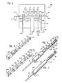
- FIG. 3 an enlarged diagrammatic view of an examplary one of the plurality of deposition chambers described hereinabove is illustrated by the reference numeral 29.
- a cathode 34 operatively disposed within the interior of the deposition chamber 29 is a cathode 34, a cathode shield 35, a power source 38, a supply conduit 36, oppositely disposed gas gates 42 and an inert sweep gas conduit 37 adjacent each gas gate 42.
- a plurality of elongated, equally spaced radiant heating elements 40 are disposed above and angled relative to the plane of the substrate 11 which assumes the normal path of travel indicated, in Figure 3, by undulating solid line 46a.
- the angular disposition of the elongated heating elements 40 whereby the heating elements 40 are closest to the substrate 11 adjacent the central portion thereof, provides a uniform temperature distribution across the transverse width of the substrate 11. This concept is fully disclosed in EP-A-0099257.
- the gas gates 42 provide relatively narrow passageways 43 operatively connecting adjacent deposition chambers such as chambers 28, 30 and 32 illustrated in Figure 2, while substantially preventing contamination due to the backflow or diffusion of reaction gas constituents from the dopant deposition chambers 28 and 32 into the intrinsic chamber 30.
- an inert gas such as argon is introduced at the high pressure (intrinsic deposition chamber) side of the gas gates 42 so that the inert gas is drawn on both sides of the web of substrate material 11 into the low pressure dopant deposition chambers 28 and 32; and (2) a plurality of magnetic elements are employed in the gate to create a magnetic field which urges the unlayered surface of the magnetic web of substrate material 11 into sliding contact with one of the passageway walls. Since the unlayered surface of the substrate 11 is urged against one wall of the passageway 43, the height of the opening may be reduced without causing the layered surface of the substrate 11 to contact and be scratched by the opposite passageway wall.
- the reduced passageway opening while making possible a substantial decrease in back-diffusion of dopant species into the intrinsic deposition chamber, does not prevent the web of substrate material from sagging (albeit a shallow sag) as it travels along its normal elongated path of travel.
- the elongated web is at an uppermost elevation when passing through the gas gates 42 and at a lowermost elevation adjacent the center of the deposition chamber.
- the shallow sag occurs despite the use of (1) a substrate moving motor driving the takeup core; (2) a substrate tensioning motor connected to the supply core; and (3) magnetic gas gates.
- the shallow sag of the substrate traveling through the chambers is not, in and of itself, harmful to the final photovoltaic device produced by the apparatus. If the elevated temperatures to which the heating elements 40 raise the web of substrate material 11, the elongated path of travel of the web, the uneven temperature distribution across the web and the force of gravity did not combine to warp the substrate 11, the web flattening apparatus of the present invention would not be necessary. However, in view of the resulting transverse undulations 46a which are defined by the warped web of substrate material 11, it is possible that semiconductor alloy layers deposited thereon could be of relatively great thicknesses in the valleys and of relatively thin thicknesses on the peaks.
- the attractive force for substantially flattening the web of substrate material 11 is established by a plurality of spaced magnets, generally 50.
- the magnets 50 are preferably fashioned from a ceramic material (such as BaO-6Fe 2 O 3 ) because such ceramic materials are inherently lightweight, relatively inexpensive, stable at elevated temperatures and capable of creating strong magnetic fields.
- the magnets 50 are illustrated in Figures 3-5 as approximately 2.5 cm wide by 2.5 cm high by 5 cm long rectangular bars, the magnets 50 are not limited (1) in dimension, (2) in configuration or (3) to a ceramic material. It is only necessary that the magnets 50 be capable of providing non-contaminating, strong substrate attractive forces at the elevated temperatures and low pressures required for the deposition of amorphous semi- conductor alloy layers onto the magnetic web of substrate material 11.
- Figure 4 illustrates a first preferred embodiment of the present invention, wherein a plurality of the generally rectangular ceramic magnets 50 are adapted to be received within an elongated, generally rectangularly-shaped, relatively thin-walled hollow tube 52.
- the hollow tube 52 is adapted to extend substantially across the transverse width of the web of substrate material 11 and to be secured, by any well known mechanical equipment, to the opposite walls of the deposition chamber.
- the tube 52 provides a convenient mechanism (1) for "stringing" a plurality of commercially available sizes of ceramic magnets 50 across the transverse width of the web of substrate material, and (2) for encapsulating the magnets 50 to prevent contamination caused by outgassing when the magnets are cyclically heated and cooled.
- the encapsulated ceramic magnets 50 For a 40 cm wide web of substrate material, at least eight (8) of the 5 cm long ceramic magnets 50 are inserted into a tube 52 which must therefore be at least 40 cm in length. An end cap 54 is used to seal the end of the tube 52 and complete the encapsulation. In order to develop a sufficiently strong attractive (magnetic) force, it has been determined that the encapsulated ceramic magnets 50 should be spaced at substantially equal, approximately 20 to 25 cm intervals along the entire longitudinal extent of the elongated path of travel of the web of substrate material 11 through each of the deposition chambers 29.
- the magnets 50 offer the additional benefit of helping to confine the plasma to the cathode region.
- the encapsulated ceramic magnets 50 are disposed at a height above the normal elongated path of travel of the web of substrate material 11 (shown by the solid line in Figure 3) of approximately 3 mm adjacent the gas gates 42 and a height of approximately 6.5 mm adjacent the center of the deposition chamber.
- the magnetic web of substrate material 11 is urged, under the tension created by the magnetic field, out of its normal path of travel and into the flat, generally planar path of travel shown by the phantom line 46b of Figure 3. Because of the magnetic field, warpage is substantially reduced, thereby providing a flat surface onto which amorphous semiconductor layers of uniform thickness can be deposited.
- Figure 5 illustrates a second preferred embodiment of the instant invention wherein an individual, relatively short, generally rectangularly-shaped, relatively thin-walled, hollow tube 52a with a correspondingly shaped end cap 54a is provided to encapsulate each one of the ceramic magnets 50.
- the number of tube-magnet assemblies in each transverse row is, as described with respect to Figure 4, sufficient to substantially extend across the transverse width of the web of substrate material 11.
- the number of rows of tube magnet assemblies and their height above the web of substrate material 11 is also the same as the number of rows and height illustrated in Figure 4 and discussed hereinabove.
- Figures 6-7 depict further embodiments of the present invention which are specially adapted for use in those mass production machines having a plurality of p-i-n type glow discharge deposition chambers in which the web of substrate material 11 follows a very lengthy path of travel.
- the multiple chamber machine it is undesirable to provide drive motors having high horsepower capabilities when that high power is necessary for the sole purpose of overcoming the initial inertial and frictional forces created by the magnetic fields acting on the magnetic web of substrate material.
- the magnetic elements take the form of one or more axially apertured, generally cylindrically-shaped, ceramic magnets 50a.
- the axial aperture 56 is adapted to receive therein an elongated axle 58.
- An elongated, hollow, generally cylindrically-shaped tube 60 having an internal diameter approximately equal to the outer diameter of the cylindrical magnets 50a, is adapted to receive therein a plurality of those cylindrical magnets 50a.
- the cylindrically-shaped tube 60 has an aperture 62 formed through the closed end 64 thereof and a corresponding aperture 70 formed through the end wall 66 of an end cap 68 which cooperates with the tube 60 to encapsulate the cylindrical magnets 50a.
- the length of the elongated tube 60 is approximately equal to the transverse width of the web of substrate material 11.
- the number of ceramic, cylindrical magnets received within the cylindrical tube 60 is dependent upon the length of each individual magnet, and must, preferably, provide an attractive field across the entire transverse width of the web of substrate material.
- (1) a sufficient number of tubular assemblies should be provided to space said assemblies at 20 to 25 cm intervals along the length of each of the deposition chambers; and (2) the assemblies should be disposed at a height above the web of substrate material of approximately 3 mm adjacent the gas gates and 6.5 mm adjacent the center of the deposition chamber.
- the tubes 60 are rotatably mounted within the deposition chamber 29.
- said assemblies rotate about the axles 58, thereby reducing the force necessary to move the web through the deposition apparatus.
- FIG. 7 a final preferred embodiment of the present invention wherein the substrate-attracting force is established by rotatably mounted electromagnetic coils (the leads to the electrical power supply are not shown), illustrated by the reference numeral 72.
- the electromagnetic coils 72 are schematically shown wrapped about metal rod 74, it should be apparent that the axle 58a, itself, could be employed to develop the magnetic field.
- an elongated, cylindrically-shaped tube 60a and a correspondingly shaped end cap 68 (which includes an end wall 66 having an aperture 70 therethrough) are adapted to receive and encapsulate the electromagnetic assembly.
- An axle 58a slides through a bore 62 in the end wall 64 of the tube 60a, the rod 74 and the apertured end cap 66 before being rotatably mounted within the deposition chamber.
- the apparatus of the present invention is adapted to substantially reduced warpage of webs of substrate material by establishing an attractive, web flattening force.
- the web is then provided with a generally planar surface, onto which uniform semiconductor layers may be deposited.
Landscapes
- Chemical & Material Sciences (AREA)
- Engineering & Computer Science (AREA)
- Physics & Mathematics (AREA)
- Analytical Chemistry (AREA)
- Plasma & Fusion (AREA)
- Materials Engineering (AREA)
- Metallurgy (AREA)
- Organic Chemistry (AREA)
- Mechanical Engineering (AREA)
- Chemical Kinetics & Catalysis (AREA)
- General Chemical & Material Sciences (AREA)
- Photovoltaic Devices (AREA)
- Manufacturing Of Magnetic Record Carriers (AREA)
- Moulds For Moulding Plastics Or The Like (AREA)
- Manufacturing Of Printed Wiring (AREA)
- Devices For Checking Fares Or Tickets At Control Points (AREA)
- Magnetic Record Carriers (AREA)
Priority Applications (1)
| Application Number | Priority Date | Filing Date | Title |
|---|---|---|---|
| AT83303993T ATE19101T1 (de) | 1982-07-12 | 1983-07-08 | Magnetisches geraet zur reduzierung der substratverwerfung. |
Applications Claiming Priority (2)
| Application Number | Priority Date | Filing Date | Title |
|---|---|---|---|
| US397190 | 1982-07-12 | ||
| US06/397,190 US4440107A (en) | 1982-07-12 | 1982-07-12 | Magnetic apparatus for reducing substrate warpage |
Publications (2)
| Publication Number | Publication Date |
|---|---|
| EP0099708A1 EP0099708A1 (en) | 1984-02-01 |
| EP0099708B1 true EP0099708B1 (en) | 1986-04-09 |
Family
ID=23570183
Family Applications (1)
| Application Number | Title | Priority Date | Filing Date |
|---|---|---|---|
| EP83303993A Expired EP0099708B1 (en) | 1982-07-12 | 1983-07-08 | Magnetic apparatus for reducing substrate warpage |
Country Status (13)
| Country | Link |
|---|---|
| US (1) | US4440107A (OSRAM) |
| EP (1) | EP0099708B1 (OSRAM) |
| JP (1) | JPS5923573A (OSRAM) |
| AT (1) | ATE19101T1 (OSRAM) |
| AU (1) | AU556673B2 (OSRAM) |
| CA (1) | CA1189174A (OSRAM) |
| DE (1) | DE3362914D1 (OSRAM) |
| IE (1) | IE54608B1 (OSRAM) |
| IL (1) | IL69153A (OSRAM) |
| IN (1) | IN158687B (OSRAM) |
| MX (1) | MX153562A (OSRAM) |
| PH (1) | PH19759A (OSRAM) |
| ZA (1) | ZA835032B (OSRAM) |
Cited By (1)
| Publication number | Priority date | Publication date | Assignee | Title |
|---|---|---|---|---|
| DE19830402A1 (de) * | 1998-07-08 | 2000-01-13 | Ardenne Anlagentech Gmbh | Verfahren und Vorrichtung zur Abscheidung von Funktionsschichten auf bewegten Substraten in einem PECVD-Prozeß |
Families Citing this family (19)
| Publication number | Priority date | Publication date | Assignee | Title |
|---|---|---|---|---|
| US4512284A (en) * | 1983-12-19 | 1985-04-23 | Rca Corporation | Glow discharge apparatus for use in coating a disc-shaped substrate |
| DE3427057A1 (de) * | 1984-07-23 | 1986-01-23 | Standard Elektrik Lorenz Ag, 7000 Stuttgart | Anlage zum herstellen von halbleiter-schichtstrukturen durch epitaktisches wachstum |
| US4664951A (en) * | 1985-07-31 | 1987-05-12 | Energy Conversion Devices, Inc. | Method provided for corrective lateral displacement of a longitudinally moving web held in a planar configuration |
| DE4324320B4 (de) * | 1992-07-24 | 2006-08-31 | Fuji Electric Co., Ltd., Kawasaki | Verfahren und Vorrichtung zur Herstellung einer als dünne Schicht ausgebildeten fotovoltaischen Umwandlungsvorrichtung |
| JPH06280026A (ja) * | 1993-03-24 | 1994-10-04 | Semiconductor Energy Lab Co Ltd | 成膜装置及び成膜方法 |
| FR2703073B1 (fr) * | 1993-03-26 | 1995-05-05 | Lorraine Laminage | Procédé et dispositif pour le revêtement en continu d'un matériau métallique en défilement par un dépôt de polymère à gradient de composition, et produit obtenu par ce procédé. |
| JP3332700B2 (ja) | 1995-12-22 | 2002-10-07 | キヤノン株式会社 | 堆積膜形成方法及び堆積膜形成装置 |
| TW303480B (en) | 1996-01-24 | 1997-04-21 | Applied Materials Inc | Magnetically confined plasma reactor for processing a semiconductor wafer |
| US6863835B1 (en) | 2000-04-25 | 2005-03-08 | James D. Carducci | Magnetic barrier for plasma in chamber exhaust |
| US20060278163A1 (en) * | 2002-08-27 | 2006-12-14 | Ovshinsky Stanford R | High throughput deposition apparatus with magnetic support |
| US20060096536A1 (en) * | 2004-11-10 | 2006-05-11 | Daystar Technologies, Inc. | Pressure control system in a photovoltaic substrate deposition apparatus |
| JP2008538450A (ja) * | 2004-11-10 | 2008-10-23 | デイスター テクノロジーズ,インコーポレイティド | 薄膜太陽電池を形成するためのパレットを基盤としたシステム |
| US20100028533A1 (en) * | 2008-03-04 | 2010-02-04 | Brent Bollman | Methods and Devices for Processing a Precursor Layer in a Group VIA Environment |
| US9252318B2 (en) * | 2008-03-05 | 2016-02-02 | Hanergy Hi-Tech Power (Hk) Limited | Solution containment during buffer layer deposition |
| US20110081487A1 (en) * | 2009-03-04 | 2011-04-07 | Brent Bollman | Methods and devices for processing a precursor layer in a group via environment |
| US8062384B2 (en) * | 2009-06-12 | 2011-11-22 | Miasole | Systems, methods and apparatuses for magnetic processing of solar modules |
| US9105778B2 (en) * | 2009-06-12 | 2015-08-11 | Apollo Precision (Kunming) Yuanhong Limited | Systems methods and apparatuses for magnetic processing of solar modules |
| JP6261967B2 (ja) * | 2013-12-03 | 2018-01-17 | 株式会社ディスコ | 加工装置 |
| CN104862650B (zh) * | 2015-05-15 | 2017-04-19 | 京东方科技集团股份有限公司 | 一种柔性基板蒸镀装置及蒸镀方法 |
Family Cites Families (11)
| Publication number | Priority date | Publication date | Assignee | Title |
|---|---|---|---|---|
| US2731212A (en) * | 1953-02-13 | 1956-01-17 | Richard S Baker | Polyphase electromagnet strip guiding and tension device |
| US2925062A (en) * | 1953-05-15 | 1960-02-16 | Heraeus Gmbh W C | Coating apparatus |
| GB1157120A (en) * | 1966-08-15 | 1969-07-02 | Templeborough Rolling Mills Lt | Methods of and apparatus for Treating Steel Rod or Wire |
| FR2043492A7 (en) * | 1970-03-26 | 1971-02-19 | Nivelet Et Barbier | Metallic strip unwinding and shearing - apparatus |
| US3661116A (en) * | 1970-11-23 | 1972-05-09 | Bethlehem Steel Corp | Magnetic stabilizing means for strip |
| LU69013A1 (OSRAM) * | 1973-03-07 | 1974-02-22 | ||
| JPS5642054B2 (OSRAM) * | 1973-07-25 | 1981-10-02 | ||
| US4410558A (en) * | 1980-05-19 | 1983-10-18 | Energy Conversion Devices, Inc. | Continuous amorphous solar cell production system |
| JPS5736437A (en) * | 1980-08-14 | 1982-02-27 | Fuji Photo Film Co Ltd | Producing device of magnetic recording medium |
| US4369730A (en) * | 1981-03-16 | 1983-01-25 | Energy Conversion Devices, Inc. | Cathode for generating a plasma |
| US4389970A (en) * | 1981-03-16 | 1983-06-28 | Energy Conversion Devices, Inc. | Apparatus for regulating substrate temperature in a continuous plasma deposition process |
-
1982
- 1982-07-12 US US06/397,190 patent/US4440107A/en not_active Expired - Lifetime
-
1983
- 1983-07-04 IL IL69153A patent/IL69153A/xx unknown
- 1983-07-07 AU AU16658/83A patent/AU556673B2/en not_active Ceased
- 1983-07-07 PH PH29189A patent/PH19759A/en unknown
- 1983-07-08 MX MX197984A patent/MX153562A/es unknown
- 1983-07-08 JP JP58124567A patent/JPS5923573A/ja active Granted
- 1983-07-08 IN IN845/CAL/83A patent/IN158687B/en unknown
- 1983-07-08 IE IE1602/83A patent/IE54608B1/en not_active IP Right Cessation
- 1983-07-08 AT AT83303993T patent/ATE19101T1/de not_active IP Right Cessation
- 1983-07-08 EP EP83303993A patent/EP0099708B1/en not_active Expired
- 1983-07-08 DE DE8383303993T patent/DE3362914D1/de not_active Expired
- 1983-07-11 ZA ZA835032A patent/ZA835032B/xx unknown
- 1983-07-12 CA CA000432237A patent/CA1189174A/en not_active Expired
Cited By (2)
| Publication number | Priority date | Publication date | Assignee | Title |
|---|---|---|---|---|
| DE19830402A1 (de) * | 1998-07-08 | 2000-01-13 | Ardenne Anlagentech Gmbh | Verfahren und Vorrichtung zur Abscheidung von Funktionsschichten auf bewegten Substraten in einem PECVD-Prozeß |
| DE19830402C2 (de) * | 1998-07-08 | 2001-02-22 | Ardenne Anlagentech Gmbh | Verfahren und Vorrichtung zur Abscheidung von Funktionsschichten auf bewegten Substraten in einem PECVD-Prozeß |
Also Published As
| Publication number | Publication date |
|---|---|
| AU1665883A (en) | 1984-01-19 |
| IN158687B (OSRAM) | 1987-01-03 |
| PH19759A (en) | 1986-06-26 |
| ZA835032B (en) | 1984-04-25 |
| IE54608B1 (en) | 1989-12-06 |
| EP0099708A1 (en) | 1984-02-01 |
| DE3362914D1 (en) | 1986-05-15 |
| US4440107A (en) | 1984-04-03 |
| CA1189174A (en) | 1985-06-18 |
| AU556673B2 (en) | 1986-11-13 |
| IL69153A0 (en) | 1983-11-30 |
| JPH0376595B2 (OSRAM) | 1991-12-05 |
| IE831602L (en) | 1984-01-12 |
| ATE19101T1 (de) | 1986-04-15 |
| IL69153A (en) | 1986-10-31 |
| MX153562A (es) | 1986-11-14 |
| JPS5923573A (ja) | 1984-02-07 |
Similar Documents
| Publication | Publication Date | Title |
|---|---|---|
| EP0099708B1 (en) | Magnetic apparatus for reducing substrate warpage | |
| US4678679A (en) | Continuous deposition of activated process gases | |
| US4664951A (en) | Method provided for corrective lateral displacement of a longitudinally moving web held in a planar configuration | |
| US4438724A (en) | Grooved gas gate | |
| CA1186787A (en) | Magnetic gas gate | |
| US4514437A (en) | Apparatus for plasma assisted evaporation of thin films and corresponding method of deposition | |
| US4600801A (en) | Fluorinated, p-doped microcrystalline silicon semiconductor alloy material | |
| EP0099257B1 (en) | Apparatus for uniformly heating a substrate | |
| EP0101286B1 (en) | Grooved gas gate | |
| US6204197B1 (en) | Semiconductor device, manufacturing method, and system | |
| JPH05121338A (ja) | 堆積膜形成方法および堆積膜形成装置 | |
| JPH0468390B2 (OSRAM) | ||
| US4609771A (en) | Tandem junction solar cell devices incorporating improved microcrystalline p-doped semiconductor alloy material | |
| EP0181113A2 (en) | Improved boron doped semiconductor materials and method for producing | |
| EP0695376B1 (en) | Magnetic roller gas gate employing transonic sweep gas flow | |
| US4574733A (en) | Substrate shield for preventing the deposition of nonhomogeneous films | |
| US4513684A (en) | Upstream cathode assembly | |
| US4608943A (en) | Cathode assembly with localized profiling capabilities | |
| EP0118643B1 (en) | Cathode assembly for glow discharge deposition apparatus | |
| EP0848434A2 (en) | Method of forming semiconductor thin film | |
| JP3017423B2 (ja) | 光起電力素子の形成方法 |
Legal Events
| Date | Code | Title | Description |
|---|---|---|---|
| PUAI | Public reference made under article 153(3) epc to a published international application that has entered the european phase |
Free format text: ORIGINAL CODE: 0009012 |
|
| AK | Designated contracting states |
Designated state(s): AT BE CH DE FR GB IT LI LU NL SE |
|
| 17P | Request for examination filed |
Effective date: 19840712 |
|
| GRAA | (expected) grant |
Free format text: ORIGINAL CODE: 0009210 |
|
| AK | Designated contracting states |
Kind code of ref document: B1 Designated state(s): AT BE CH DE FR GB IT LI LU NL SE |
|
| PG25 | Lapsed in a contracting state [announced via postgrant information from national office to epo] |
Ref country code: BE Effective date: 19860409 Ref country code: AT Effective date: 19860409 |
|
| REF | Corresponds to: |
Ref document number: 19101 Country of ref document: AT Date of ref document: 19860415 Kind code of ref document: T |
|
| PG25 | Lapsed in a contracting state [announced via postgrant information from national office to epo] |
Ref country code: SE Effective date: 19860430 |
|
| ITF | It: translation for a ep patent filed | ||
| REF | Corresponds to: |
Ref document number: 3362914 Country of ref document: DE Date of ref document: 19860515 |
|
| ET | Fr: translation filed | ||
| PG25 | Lapsed in a contracting state [announced via postgrant information from national office to epo] |
Ref country code: LU Free format text: LAPSE BECAUSE OF NON-PAYMENT OF DUE FEES Effective date: 19860731 |
|
| PGFP | Annual fee paid to national office [announced via postgrant information from national office to epo] |
Ref country code: NL Payment date: 19860731 Year of fee payment: 4 |
|
| PLBE | No opposition filed within time limit |
Free format text: ORIGINAL CODE: 0009261 |
|
| STAA | Information on the status of an ep patent application or granted ep patent |
Free format text: STATUS: NO OPPOSITION FILED WITHIN TIME LIMIT |
|
| 26N | No opposition filed | ||
| PG25 | Lapsed in a contracting state [announced via postgrant information from national office to epo] |
Ref country code: LI Effective date: 19870731 Ref country code: CH Effective date: 19870731 |
|
| PG25 | Lapsed in a contracting state [announced via postgrant information from national office to epo] |
Ref country code: NL Effective date: 19880201 |
|
| NLV4 | Nl: lapsed or anulled due to non-payment of the annual fee | ||
| REG | Reference to a national code |
Ref country code: CH Ref legal event code: PL |
|
| ITTA | It: last paid annual fee | ||
| PGFP | Annual fee paid to national office [announced via postgrant information from national office to epo] |
Ref country code: GB Payment date: 20000614 Year of fee payment: 18 |
|
| PGFP | Annual fee paid to national office [announced via postgrant information from national office to epo] |
Ref country code: FR Payment date: 20000707 Year of fee payment: 18 |
|
| PGFP | Annual fee paid to national office [announced via postgrant information from national office to epo] |
Ref country code: DE Payment date: 20000727 Year of fee payment: 18 |
|
| PG25 | Lapsed in a contracting state [announced via postgrant information from national office to epo] |
Ref country code: GB Free format text: LAPSE BECAUSE OF NON-PAYMENT OF DUE FEES Effective date: 20010708 |
|
| GBPC | Gb: european patent ceased through non-payment of renewal fee |
Effective date: 20010708 |
|
| PG25 | Lapsed in a contracting state [announced via postgrant information from national office to epo] |
Ref country code: FR Free format text: LAPSE BECAUSE OF NON-PAYMENT OF DUE FEES Effective date: 20020329 |
|
| PG25 | Lapsed in a contracting state [announced via postgrant information from national office to epo] |
Ref country code: DE Free format text: LAPSE BECAUSE OF NON-PAYMENT OF DUE FEES Effective date: 20020501 |
|
| REG | Reference to a national code |
Ref country code: FR Ref legal event code: ST |