EP0098723B1 - Contrôle automatique de couleur pour un récepteur de télévision digital - Google Patents
Contrôle automatique de couleur pour un récepteur de télévision digital Download PDFInfo
- Publication number
- EP0098723B1 EP0098723B1 EP83303701A EP83303701A EP0098723B1 EP 0098723 B1 EP0098723 B1 EP 0098723B1 EP 83303701 A EP83303701 A EP 83303701A EP 83303701 A EP83303701 A EP 83303701A EP 0098723 B1 EP0098723 B1 EP 0098723B1
- Authority
- EP
- European Patent Office
- Prior art keywords
- digital
- signal
- chroma
- signals
- burst
- Prior art date
- Legal status (The legal status is an assumption and is not a legal conclusion. Google has not performed a legal analysis and makes no representation as to the accuracy of the status listed.)
- Expired
Links
Images


Classifications
-
- H—ELECTRICITY
- H04—ELECTRIC COMMUNICATION TECHNIQUE
- H04N—PICTORIAL COMMUNICATION, e.g. TELEVISION
- H04N9/00—Details of colour television systems
- H04N9/64—Circuits for processing colour signals
- H04N9/68—Circuits for processing colour signals for controlling the amplitude of colour signals, e.g. automatic chroma control circuits
Definitions
- the present invention relates to automatic color control for a digital television receiver and, in particular, to digital chroma gain control apparatus.
- an analog video signal for example, the baseband video signal
- ADC analog-to-digital
- the digital samples are processed in a digital comb filter to produce digital samples representing separated luminance and chrominance information.
- the digital luminance and chrominance samples are processed in respective channels of a digital signal processing section which perform functions similar to those performed by analog luminance and chrominance channels found in presently commercially available television receivers.
- the digital samples produced by the luminance and chrominance channels of the digital signal processing section are converted into analog signals representing image display information. The conversion is performed by digital-to-analog converters (DAC) the outputs of which are coupled to a kinescope in conventional fashion.
- DAC digital-to-analog converters
- the Nyquist sampling criteria requires that the frequency at which the analog baseband signal is sampled must be at least twice the highest frequency of interest of the analog baseband video signal. Because it is desirable that the sampling signal be consistently related in phase to the analog baseband video signal in order not to introduce distortion in the reproduced image, the sampling signal is derived from the color reference burst signal component of the baseband video signal.
- the frequency of the color reference burst signal is usually referred to as the color subcarrier frequency f sc .
- the sampling signal may be derived by an arrangement which extracts the color reference burst component from the baseband video signal and a phase-locked loop (PLL) which locks an oscillator to an integer multiple of the subcarrier frequency f sc of the reference burst signal.
- PLL phase-locked loop
- the highest baseband video signal frequency of interest is around 4.2 MHz and the color subcarrier frequency f sc is approximately 3.58 MHz. Accordingly, the lowest sampling signal frequency at an integer multiple of the color burst signal which satisfies the Nyquist criterion is 3f sc f. Because demodulation of color burst signals, as described below, can more readily be realized when the sampling signal is an even multiple of the color subcarrier frequency, the most often proposed sampling frequency is 4f so (approximately 14.32 MHz).
- One function performed by the chrominance channel of the digital signal processing section is color demodulation by which the digital chrominance samples occurring at times corresponding to predetermined phase angles of the color reference burst component associated with respective color demodulation color reference vectors are selected and provided at respective outputs.
- the resultant digital samples can then be used to produce color signals for determining the color content of the reproduced image.
- the color reference vectors chosen for color demodulation correspond either to the 0° and 90° phase points or to the 57° and 147° phase points with respect to the color reference burst signal.
- the former are commonly referred to as the -(B-Y) and (R-Y) color reference vectors and the latter are commonly referrd to as the I and Q color reference vectors.
- the human eye is more sensitive to such signals because the I signal corresponds to flesh tones.
- the chrominance channel of the digital signal processing section be responsive to user controls for adjusting the tint or hue of the reproduced image as desired.
- color demodulation is accomplished by aligning the phase of the sampling signal so that samples are produced by the A/D converter at times corresponding to the phase angles of the color burst signal associated with the I, Q, -1 and -Q color reference vectors. The samples which occur at times corresponding to the I and Q color reference vectors are selectively demodulated and provided at respective I and Q outputs. Tint control is accomplished by adjusting the phase angle of the sampling signal relative to the phase of the color reference burst signal.
- the automatic color control apparatus includes a burst sampler which examines the peak magnitude of digital chrominance channel samples which occur during the color burst interval. The peak digital chrominance burst samples are compared to a digital reference level to generate a color amplitude control signal.
- the phase of the sampling signal is aligned so that digital samples corresponding to the peaks of the color burst signal are available in order to obtain the highest possible amplitude for the samples and therefore improve the noise performance of the system.
- the peaks of the color burst signal occur at 360° multiples of the 0° phase point thereof which corresponds to the -(B-Y) color reference vector.
- a digital color television signal processing system including an arrangement for determining the amplitude of the color burst signal for the purpose of chrominance gain control which is not disturbed by the phase of the sampling signal being varied for the purpose of tint control.
- German published application DE-A1-2854236 discloses a digital TV receiver in which digital chroma signals are supplied to gain controlled processing means including means for producing a chroma signal scaled in response to a chroma control signal but it does not consider the requirements associated with the generation of the chroma control signal.
- a digital chroma gain control apparatus for a television system wherein the magnitude of a digital chroma reference burst component of sampled digital chroma signals is determined from first and second digital chroma reference signals which are in quadrature with respect to each other.
- first and second digital chroma reference signals are produced by sampling the chroma reference burst component of the digital chroma signals and a digital sum indicative of the magnitude of the sum of the respective squares of the magnitudes of the first and second digital chroma reference signals is developed.
- a chroma control signal is produced in response to the digital sum signal departing from a predetermined value for causing a processing device to scale the chroma signals to have a predetermined magnitude.
- the broad arrows represent digital data connections for passing digital words having eight bits in parallel, unless a different arrangement is specified.
- IF signal processor 14 supplies the IF signal to video detector 16 which develops a composite baseband video signal therefrom.
- Tuner 12, IF processor 14 and video detector 16 can be of conventional implementation as used in presently commercially available television receivers.
- Timing signals for digital processing are developed by clock generator 18 in response to the composite video signal, one horizontal line (1 H) of which is shown in FIGURE 3a.
- Each horizontal line 1H includes a horizontal blanking interval 300 during which no image information is present.
- Horizontal blanking interval portion 300 includes horizontal synchronizing pulse 302 followed by a color subcarrier reference burst signal 304 including a minimum of eight cycles of the 3.58 MHz color subcarrier signal.
- the remaining portion 306 of horizontal line 1H provides image information in accordance with the NTSC standards in which the luminance (brightness) information is related to amplitude and in which the chrominance (color) information modulates the 3.58 MHz subcarrier.
- FIGURE 2 shows the relative phases of the chroma reference vectors with the -(B-Y) component being defined at 0° phase with respect to the positive peak of the chroma reference burst signal.
- the I component is retarded by 57° and is in quadrature with-the Q component which is further retarded by 90°, i.e. at 147°.
- the -I and -Q components are 180° out of phase with the I and Q components, respectively.
- the R-Y, B-Y and -(R-Y) components are at 90°, 180° and 270° phase angles, respectively.
- Clock generator 18 provides a burst gate signal shown in FIGURE 3b which includes a pulse 310 of duration less than that of the color subcarrier reference burst signal 304 and which is positioned in time, for example, by predetermined delay after horizontal sync pulse 302.
- a phase-locked loop (PLL) included in clock generator 18 produces a clock signal at 4f so which is phase locked to the color subcarrier reference burst signal with phase correction being made during the time interval defined by pulse 310 of the burst gate signal. Phase lock is maintained by the PLL throughout the horizontal line 1H.
- Phase shifter 20 provides advancement or retardation of the phase of the 4f sc clock signal in relation to the phase of color subcarrier burst signal f sc in response to a tint reference signal which is manually adjustable by the user.
- the 4f so clock signal at the output of phase shifter 20 is shifted in phase relative to the phase of the color subcarrier reference burst signal f sc by 57° plus or minus the user introduced variation tp control tint.
- it is unimportant whether the nominal 57° phase lag is provided by ctock generator 18 or by phase shifter 20.
- the composite video signal from video detector 16 is also applied to analog-to-digital converter 24 which also receives the 4f sc clock signal and converts the analog baseband composite video signal to representative eight-bit digital samples at the 4f sampling frequency.
- Each digital sample includes a group of eight bits representing the magnitude and polarity of the baseband video signal at the time the sample is taken.
- the eight-bit samples employed in the arrangement herein described provides satisfactory signal resolution.
- the present invention may be employed with arrangements which process digital words having greater or lesser numbers of bits.
- Digital video samples from ADC 24 are coupled to digital comb filter 26 which produces digital samples Y representative of luminance informa- ton and digital samples C representative of chrominance information.
- Digital comb filter 26 includes, for example, a delay element comprising a 910-stage, eight-bit parallel shift register (not shown) to provide a 1 H time delay in the NTSC system using the 4f sc sampling frequency.
- the delayed digital samples produced at the output of the 910-stage shift register are combined with undelayed digital samples by an adder (not shown) to produce digital luminance samples (Y) and are combined by a subtractor (not shown) to produce digital chrominance samples (C).
- Luminance processor 50 receives digital luminance samples Y and processes them in response to the 4f sr sampling signal.
- the processed luminance digital signals are applied to digital-to-analog converter and low pass filter 52 to develop an analog luminance signal Y'.
- Digital chrominance samples C are processed by chrominance processor 90, including chroma amplifier and peaker 28, I demodulator and low pass filter 30, and Q demodulator and low pass filter 32, to develop I and Q digital chroma signals.
- chroma processor 90 The operation of chroma processor 90 is described in detail below.
- the I and Q digital chrominance signals are applied to digital-to-analog converters and low pass filters 54 and 56, respectively, which produce analog chroma signals I' and Q', respectively.
- Matrix 58 receives the analog luminance signal Y' and analog chroma signals I' and Q' and develops, in conventional fashion, red R, green G and blue B signals which are applied to kinescope KS.
- Deflection processor 60 produces horizontal and vertical deflection signals which are applied to kinescope deflection yoke DY in response to the synchronizing information encoded in the digital video samples produced by ADC 24.
- the raster produced on kinescope KS in response to the signals applied to deflection yoke DY cooperates with the R, G, and B signals to produce an image display on KS in conventional fashion.
- Digital chrominance processor 90 of FIGURE 1 operates in response to the sampling signal 4f sc received from phase shifter 20 and the digital chrominance samples C received from comb filter 26.
- Sampling signal 4f sc shown in FIGURE 4b is nominally shifted by 57° with respect to the phase of reference burst signal 304 shown in FIGURE 4a so as to occur at times corresponding to the I, Q, -I and -Q vectors, as shown in FIGURE 2.
- FIGURE 4 depicts signal waveforms in a time interval within a portion of the horizontal blanking interval 300 of horizontal line 1H shown in FIGURE 3; this time relationship is indicated by the phantom lines with arrowheads pointing between FIGURES 3 and 4.
- the timing signals shown in FIGURES 4b, 4c and 4d are present throughout the entire horizontal line 1H thereby producing a series of digital chroma samples I and Q shown in FIGURES 4h and 4i throughout each horizontal line 1 H.
- the values of the I and Q samples will be zero during horizontal blanking interval 300 except during the portion thereof when color reference burst 304 is present. Picture information is not present during blanking interval 300 but is present during the remaining portion 306 of horizontal line 1 H.
- Digital chrominance samples C are processed by chroma amplifier and peaker 28, shown in detail in FIGURE 5, which provides scaling of the magnitudes of chrominance samples C.
- Coarse gain shifter 110 comprises a controllable, eight-bit parallel shift register controlled by shift signals provided by microprocessor 120. The magnitude of chroma digital words C is increased in increments of 6dB for each shift to the left by one bit position (e.g., to a more significant bit location) provided by gain shifter 110. Conversely, the magnitude of chroma sample C is decreased in increments of 6dB for each shift to the right by one bit location.
- Chroma words produced at the output of gain shifter 110 are applied to chroma bandpass filter 112 which may comprise, for example, a finite impulse response (FIR) filter. Chroma samples from bandpass filter 112 are coupled to fine gain section 113 in which they are applied to the address inputs of random access memory (RAM) 114 and to one input of adder 116.
- RAM 114 is an eight-bit by 256 register memory. The output from RAM 114 is coupled to a second input of adder 116. The sum produced by adder 116 is then coupled to I demodulator 30 and Q demodulator 32 of FIGURE 1.
- microprocessor 120 calculates the required gain and controls gain shifter 110 to produce the required number of shifts left or right to achieve the 6 dB gain increment next below the required scaling.
- Microprocessor 120 calculates a scaling factor having a value between one and two which will cause fine gain section 113 to exhibit the gain which, in combination with coarse gain shifter 110, produces the required gain.
- a table of scaling values comprising the RAM addresses times the scaling factor developed by microprocessor 120 is loaded into buffer register 122.
- Register 122 has 256 eight-bit register locations corresponding to the addressable registers of RAM 114. At the appropriate time, such as during the vertical blanking interval, microprocessor 120 enables RAM 114 to be loaded with the table of scaling values stored in buffer register 122.
- gain shifter 110 is controlled to produce two left shifts of the digital chroma samples C to provide a gain of +12 dB.
- the table of scaling values calculated for RAM 114 then corresponds to a scaling factor of one-third.
- Chroma samples C scaled by one-third by RAM 114 when added to the chroma samples C from bandpass filter 112 by adder 11.6, produce chroma samples scaled by a value of four-thirds, which corresponds to a gain of 2.5 dB.
- Patent Application Serial Number 359,433 of Lewis, Jr et al entitled DIGITAL TELEVISION RECEIVER AUTOMATIC CHROMA CONTROL SYSTEM corresponding to GB-A-2118800 provides a more detailed description of an embodiment of chroma amplifier and peaker 28 of the sort described herein.
- I and Q clock generator 22 develops I clock and Q clock signals shown in FIGURES 4c and 4d, respectively, in response to sampling signal 4f sc .
- the I clock signal is at a high level at times corresponding to the I phase of the reference burst signal 304 and the Q clock signal is at a high level at times corresponding to the Q phase thereof.
- the I clock and Q clock signals are therefore in quadrature with each other and nominally at 57° and 147°, respectively, with respect to the phase of the color subcarrier signal f sc as is required for demodulation and sampling of the I and Q digital samples.
- Digital chroma signals from chroma amplifier and peaker 28 are applied to I demodulator and low pass filter 30 shown in FIGURE 6.
- Chroma samples C are applied to a nine-stage, eight-bit parallel shift register 200 and are shifted therethrough in response to the I clock signal applied to each stage thereof.
- the digital values of +1 samples are stored in each of the nine stages of shift register 200 and are applied to the corresponding ones of the nine weighting devices 202.
- Each weighting device 202 is, for example, a multiplier which multiplies the +1 sample digital word applied at its input by the weighting value shown within the blocks in FIGURE 6.
- the respective weighted digital values from weighting devices 202 are summed by a nine-input, eight-bit adder 204 and are applied to signal averager 206.
- Averager 206 may simply be a latch to avoid producing erroneous I values during the time required for multipliers 202 and adder 204 to settle.
- This arrangement 30 provides low pass filtering to produce demodulated digital chroma signals I.
- Q demodulator and low pass filter 32 is implemented similarly to the I demodulator and low pass filter 30 just described except that its shift register is clocked by the Q clock and its output signal is the demodulated digital chroma signal Q.
- Digital chroma signals I and Q shown in FIGURES 4h and 4i, comprise respective series of eight-bit digital words representing the +1 sample values, and the +Q sample values. The value of each digital word is unchanged during the time intervals defined between the vertical dividing lines in FIGURES 4h and 4i corresponding in time with the I clock and Q clock signals.
- the digital values of the I and Q samples occurring during the reference burst signal 304 are employed for automatically controlling the chrominance processor gain.
- This sampling interval corresponds to the duration of burst gate pulse 310 shown in FIGURE 4e which is selected to include a number of the at least eight cycles of the reference burst signal 304, but excluding at least the first and last cycle thereof. This exclusion avoids error which would be introduced owing to the attack time and decay times of reference burst signal 304, i.e. because it is not at its full amplitude during its first and last cycles.
- the value of digital chroma signal I is sampled and stored by I burst latch 36 during the interval defined by burst gate pulse 310 in response to sample signal SI which includes I sampling pulse 312 shown in FIGURE 4f.
- the value of digital chroma signal Q is sampled and stored in Q burst latch 42 in response to sample signal SQ which includes Q sampling pulse 314 shown in FIGURE 4g.
- Latches 36 and 42 are eight-bit parallel latches.
- Sampling signal SI is developed by I burst strobe 34 shown in FIGURE 7.
- Burst gate pulse 310 is applied to set input S offlip flop FF1 to apply a high logic level from output Q of FF1 to a first input of AND gate 102.
- I sampling pulse 312 is developed at the output of AND gate 102. That I sampling pulse is applied, after a suitable delay 104, to the reset input R of FF1 causing its Q outputto become a low logic level.As a result, coincidence at the inputs of AND gate 102 is lost thereby terminating sampling pulse 312.
- a suitable delay is introduced, for example, by a plurality of inverters 104.
- Q burst strobe 40 is of similar structure to that of I burst strobe 34 except that it responds to the Q clock signal to develop sampling pulse 314 of the SQ sampling signal shown in FIGURE 4g.
- a digital word representing the value of the +1 chroma signal sample corresponding to the reference burst signal 304 during time interval 310 is stored in I burst latch 36, and a digital word representing the value ofthe +Q chroma signal sample atthattime is stored in Q burst latch 42.
- I burst squarer 38 receives the stored +1 chroma reference sample from I burst latch 36, develops a digital word corresponding to the square thereof, and applies that squared +I reference sample to a first input of adder 46.
- Q burst squarer 44 receives the value of the stored +Q chroma reference sample, develops the square thereof, and applies that squared +Q reference sample to a second input of adder 46.
- Adder 46 provides a digital word corresponding to the sum of the squared +1 chroma reference sample and the squared +Q chroma reference sample to digital comparator 48.
- square of an eight-bit word can be a sixteen-bitword.
- squarers 38 and 44, adder 46 and comparator 48 can be sixteen-bit devices. But, lesser numbers of bits will provide sufficient resolution to satisfactorily control chroma gain. Therefore, only the eight most significant bits are employed and eight-bit devices are satisfactory.
- Each of I burst squarer 38 and Q burst squarer 44 comprises, for example, a read only memory (ROM) having 256 addressable registers each of which stores an eight-bit digital word corresponding to the eight most significant bits of the square of its address.
- the +I and +Q digital chroma reference samples are applied to the address inputs of the respective I and Q ROMs 38 and 44 causing each ROM to produce at its output a digital word whose value represents the square of the chroma reference sample applied as the register address.
- Digital magnitude comparator 48 receives a chroma reference word corresponding to a predetermined desired amplitude of the reference burst signal 304, for example, nominally 20 IRE units zero-to-peak in an NTSC TV system in which one volt peak-to-peak corresponds to 140 IRE units.
- the chroma reference word is compared to the eight most significant bits of the squared chroma reference sum produced by adder 46.
- the chroma reference word value is responsive, at least in part, to a user adjustment for color level.
- Comparator 48 produces an automatic chroma control signal,E which indicates departure of the squared chroma reference sum value from the predetermined chroma reference word value.
- control signal E is a two-bit parallel word'having, for example, the value 00 indicating no departure, 10 indicating that the squared chroma reference sum value exceeds that of the chroma reference word value, and 01 indicating that the chroma reference word value exceeds the squared chroma reference sum value.
- Microprocessor 120 in chroma amplifier and peaker 28 (FIGURE 5) responds to these two flag bits by incrementing or decrementing the scaling factor each time a comparison is made by digital comparator 48, e.g., at the horizontal line rate 1H or at the vertical field rate.
- automatic chroma control signal E can be an eight-bit word representing the value of the difference between the squared chroma reference sum value and the chroma reference word value.
- microprocessor 120 calculates the required scaling factor and adjusts the scaling factor table for RAM 114 to substantially eliminate the amplitude deviation of the chroma reference signal. I.e. microprocessor 120 causes RAM 114 to be loaded with a scaling factor table which makes the range of possible values of chroma samples C correspond to a predetermined range of values.
- microprocessor 120' directly receives the chroma reference word value and the values of the I and Q chroma reference samples stored in I burst latch 36 and in Q burst latch 42, respectively.
- Microprocessor 120' in addition to the operations previously described, performs the squaring operation described in relation to I burst squarer 38 and Q burst squarer 44, the addition operation described in relation to adder 46, and the magnitude comparison described in relation to digital comparator 48.
- Equation 1 mathematically reduces to It is noted that the digital value of the squared reference chroma sum produced by adder 46 is responsive to the amplitude of the chroma reference burst signal 304 and is unaffected by the particular phase angle X at which chroma reference burst signal 304 is sampled. Therefore, tint control accomplished by adjusting the phase angle of the sampling signal 4f sc relative to the phase of the color burst reference signal 304 will not disturb operation of the automatic chroma control arrangement of the present invention.
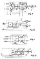
- FIGURE 9 shows an arrangement in which I burst squarer 38' and Q burst squarer 44' employ a single ROM 140 in place of the two separate ROMs 38 and 44 described above.
- I burst latch 36' is an eight-bit parallel latch which stores the I reference sample applied to its input in response to pulse 312 of sampling signal SI which is applied to its strobe terminal ST.
- Latch 36' supplies the stored word at its output terminal in response to pulse 320 of timing signal T1, shown in FIGURE 3c, applied to its output enable terminal OE.
- Eight-bit parallel Q burst latch 42' stores a Q reference sample in response to pulse 314 of sampling signal SQ which is applied to its strobe terminal ST and provides the stored Q reference sample at its output terminal in response to pulse 322-of signal T2, shown in FIGURE 3d, applied to its output enable terminal OE.
- ROM 140 has 256 addressable registers each of which stores an eight-bit digital word corresponding to the eight most significant bits of the square of its address.
- ROM 140 receives the stored I reference sample and develops the square thereof which is stored in I-squared latch 142.
- ROM 140 receives the stored Q reference sample and produces the square thereof which is stored in Q-squared latch 144.
- the squared I reference sample stored in I-squared latch 142 is applied to a first input of eight-bit parallel adder 46 and the squared Q reference sample stored in Q-squared latch 144 is applied to a second input thereof.
- the sum developed at the output of adder 46 is applied to latch 47 in which it is stored during the interval defined by pulse 324 of signal T3, shown in FIGURE 3e.
- Pulses 320, 322 and 324 may be developed, for example, by appropriate delays referenced, to horizontal synchronizing pulse 302 or to the burst gate pulse 310. These delays are conveniently realized by counting down sampling clock 4f sc . The order in which pulses 320 and 322 are developed is immaterial, however, pulse 324 must be developed thereafter to control latch 47. This arrangement prevents erroneous sums developed by adder 46 during the time sequencing of ROM 140 by T1 and T2 from being supplied to comparator 48.
- FIGURE 10 shows a modification in which I burst strobe 34 and Q burst strobe 40 are replaced by strobe generator 35.
- Flip flop FF1, AND gate 102 and delay elements 104 produce a pulse at the output of AND gate 102 as described above in relation to FIGURE 7. That pulse is delayed in time by delay device 152 to produce common sampling signal SC shown in FIGURE 4j.
- Delay interval 51 is selected so that the single pulse of sampling signal SC occurs at a time when both the I samples and Q samples shown in FIGURE 4h and 4i are present and unchanging.
- sampling single SC can be applied to both I burst latch 36 and Q burst latch 42 to sample both the I and Q reference signals simultaneously.
- FIGURES 11 and 12 show a modification in which a plurality of I reference samples and Q reference samples are taken and an average value for each is determined. This arrangement advantageously reduces the effect of any errors introduced by random deviations which might be present in any particular sample of the chroma reference burst signal 304 caused, for example, by noise.
- Sampling pulses SI' and SQ' shown in FIGURES 4k and 4m are developed by the arrangement shown in FIGURE 11.
- the I clock signal and the Q clock signal are respectively applied to set input S and reset input R of flip flop FF2 to produce out-of-phase clock signals at the outputs Q and Q thereof.
- the clocking signal developed at output Q of FF2 is passed by AND gate 160 to become sampling signal SI' during the time interval when burst gate pulse 310 is applied to the second input of AND gate 160.
- the clocking signal at the Q output of FF2 is passed by AND gate 164 to develop sampling signal SQ' during a time interval of equal duration to that of burst gate pulse 310.
- Delay device 162 is interposed to delay application of burst gate pulse 310 to the input of AND gate 164.
- Delay device 162 is provided so that an equal number of I reference samples and Q reference samples will be obtained, e.g., four samples.
- Delay interval ⁇ 2 is selected to be of sufficient duration to avoid generation of a sampling pulse in sampling signal SQ' during the interval 62 immediately following the rising edge of burst gate pulse 310, as shown in FIGURE 4m.
- FIGURE 12 shows modified I burst latch 36" which, in addition to latching the I chroma reference sample, receives a plurality of I chroma reference samples and develops a digital word representative of the average of those samples.
- latch 184 initially stores a zero value to which it has been a reset by horizontal drive signal H.DR. which is applied to its reset input R in response to horizontal synchronizing pulse 302.
- a first I chroma reference sample is applied to an input of parallel adder 182.
- Adder 182 produces a digital word equal to the sum of the digital words applied to its inputs from I sample demodulator 30 and latch 184. This sum is thereafter stored by latch 184 in response to inverted sampling signal SI' provided to its strobe terminal ST by inverter 186.
- Q burst latch 42 is replaced by structure identical to that of latch 36' but which receives Q reference samples and sampling signal SQ'.
- adder 182 is an ten-bit parallel adder and latch 184 is an ten-bit parallel latch. Satisfactory accuracy is-obtained, however, when an eight-bit word is supplied to ROM 38". This is conveniently accomplished by using the eight most significant bits from latch 184. Fortuitously, when four samples are to be averaged, discarding the two least significant bits of the word stored in latch 184 has the same effect as shifting to the right by two bit positions which is equivalent to dividing by four. Therefore, the eight-bit word supplied to ROM 38" is the average of the four I chroma samples.
- each of the addressable registers in ROM 38" can be loaded with a digital word corresponding to the square of its address divided by the square of the number of samples taken during the averag-. ing operation.
- the squared addresses would be divided by 16 and the quotient thereof loaded into the respective registers of ROM 38".
- the same end could be achieved by increasing the value of the chroma reference word applied to digital comparator 48 by a multiplying factor equal the square of the number of samples averaged.
- sampling signals SI' and SQ' can be modified to include eight pulses to cause eight I and eight Q reference samples to be averaged within four cycles of chroma reference burst signal 304.
- control signal E developed by digital comparator 48 of FIGURE 1 is converted to an analog gain control signal by a digital-to-analog converter (not shown).
- the analog gain control signal is applied to at least one of tuner 12, IF processor 14, and video detector 16 which include conventional gain varying arrangements such as those found in commercially available television receivers.
- ADC 24 includes a reference voltage source (not shown) to which the analog baseband composite video signal is compared.
- the range of input voltages applied to 4DC 24 to obtain the full eight-bit digital range of its digital output word is directly dependent upon the magnitude of that reference voltage. I.e. the scaling factor of ADC 24 directly depends upon its reference voltage.
- automatic chroma control signal E developed by digital magnitude comparator 48 is applied via digital data bus 62 (shown in phantom) to the reference voltage source of ADC 24. Since control signal E is a digital word representing the departure of error in the chroma signal level, it can be applied to produce an analog voltage which is employed as all or part of the reference voltage of ADC 24. Control signal E is poled to increase the reference voltage of ADC 24 when the analog signal is too large to thereby decrease the scaling factor, and vice versa. This modification performs adjustment of the digital signal levels of luminance Y and chrominance C digital signals as well as of the digital signals supplied to deflection processor 60.
- the squaring arrangement shown in FIGURE 9 in conjunction with the averaging latch arrangement 36' shown in FIGURE 12.
- the squaring operation e.g., as performed by ROM 38" in FIGURE 12 or the equivalent embodiment shown in FIGURE 9
- the squaring operation can be performed directly on the I chroma reference samples and the averaging operation performed thereafter by averaging arrangement 36'. It appears, however, that errors introduced by random effects such as noise are less pronounced in the preferred arrangement in which the averaging operation preceeds the squaring operation.
- pulses 312 and 314 of sampling signals SI and SQ of FIGURES 4f and 4g may be developed at other times during the time interval defined by burst gate pulse 310 of FIGURE 4e. Any delays which maintain the proper relation between pulses 312 and 314 and the phase of the color reference burst signal 304 are satisfactory.
- Squarers 38 and 44 may each employ an eight bit multiplier, such as the TDC 1008J commercially available from TRW Inc., having the stored I and Q values applied to both of their inputs, respectively.
- TDC 1008J commercially available from TRW Inc.
Landscapes
- Engineering & Computer Science (AREA)
- Multimedia (AREA)
- Signal Processing (AREA)
- Processing Of Color Television Signals (AREA)
Claims (12)
Applications Claiming Priority (4)
| Application Number | Priority Date | Filing Date | Title |
|---|---|---|---|
| US39483982A | 1982-07-02 | 1982-07-02 | |
| US394839 | 1982-07-02 | ||
| US437825 | 1982-10-29 | ||
| US06/437,825 US4482916A (en) | 1982-07-02 | 1982-10-29 | Automatic color control for a digital television receiver |
Publications (2)
| Publication Number | Publication Date |
|---|---|
| EP0098723A1 EP0098723A1 (fr) | 1984-01-18 |
| EP0098723B1 true EP0098723B1 (fr) | 1986-07-30 |
Family
ID=27014885
Family Applications (1)
| Application Number | Title | Priority Date | Filing Date |
|---|---|---|---|
| EP83303701A Expired EP0098723B1 (fr) | 1982-07-02 | 1983-06-27 | Contrôle automatique de couleur pour un récepteur de télévision digital |
Country Status (5)
| Country | Link |
|---|---|
| US (1) | US4482916A (fr) |
| EP (1) | EP0098723B1 (fr) |
| JP (1) | JPS59501389A (fr) |
| DE (1) | DE3364939D1 (fr) |
| WO (1) | WO1984000273A1 (fr) |
Families Citing this family (12)
| Publication number | Priority date | Publication date | Assignee | Title |
|---|---|---|---|---|
| US4673970A (en) * | 1984-06-08 | 1987-06-16 | Matsushita Electric Industrial Co., Ltd. | Chrominance signal processing system |
| NL8402286A (nl) * | 1984-07-19 | 1986-02-17 | Philips Nv | Kleurentelevisieontvanger bevattende een chrominantiesignaalverwerkingsschakeling en een geintegreerde schakeling daarvoor. |
| EP0226649B1 (fr) * | 1985-12-19 | 1989-08-09 | Deutsche ITT Industries GmbH | Circuit de réglage de chrominance d'un récepteur numérique de télévision |
| US5187568A (en) * | 1991-10-03 | 1993-02-16 | Zenith Electronics Corporation | Video processor having improved clamping system for color television receivers |
| KR0165281B1 (ko) * | 1992-11-24 | 1999-03-20 | 김광호 | 색 버스트신호의 이득검출방법 및 그 장치 |
| JPH06243580A (ja) * | 1993-02-15 | 1994-09-02 | Hitachi Ltd | Agc回路 |
| US5777688A (en) * | 1995-05-11 | 1998-07-07 | Matsushita Electric Industrial Co., Ltd. | Signal processor |
| US5675339A (en) * | 1995-07-31 | 1997-10-07 | Harris Corporation | A/D reference level adjustment circuit to maintain optimum dynamic range at the A/D |
| FR2739519B1 (fr) * | 1995-09-29 | 1997-12-12 | Sgs Thomson Microelectronics | Dispositif de correction de teinte d'un signal de television selon la norme ntsc |
| US6031478A (en) * | 1998-02-19 | 2000-02-29 | Nortel Networks Corporation | Dynamic range extension of wideband receiver |
| US6333707B1 (en) * | 1998-02-19 | 2001-12-25 | Nortel Networks Limited | Dynamic range extension of wideband receiver |
| JP3895887B2 (ja) * | 1999-06-25 | 2007-03-22 | 日本電気株式会社 | デシベルレベル調整装置 |
Family Cites Families (9)
| Publication number | Priority date | Publication date | Assignee | Title |
|---|---|---|---|---|
| US3732358A (en) * | 1969-05-08 | 1973-05-08 | Rca Corp | Automatic chroma control circuits |
| US3962723A (en) * | 1973-10-25 | 1976-06-08 | Gte Sylvania Incorporated | Automatic peak color control circuit |
| JPS6024429B2 (ja) * | 1977-08-15 | 1985-06-12 | 沖電気工業株式会社 | デイジタル走査変換方式 |
| FR2428348A1 (fr) * | 1978-06-08 | 1980-01-04 | Trt Telecom Radio Electr | Regulateur numerique du niveau d'un signal multiplex en frequence |
| DE2854236C2 (de) * | 1978-12-15 | 1982-06-09 | Deutsche Itt Industries Gmbh, 7800 Freiburg | Farbfernsehempfänger mit mindestens teilweise digitaler Signalverarbeitung und mit mindestens einer integrierten Schaltung für das Luminanzsignal und die Chrominanzsignale |
| US4250458A (en) * | 1979-05-31 | 1981-02-10 | Digital Communications Corporation | Baseband DC offset detector and control circuit for DC coupled digital demodulator |
| US4270177A (en) * | 1979-06-20 | 1981-05-26 | Tokyo Shibaura Denki Kabushiki Kaisha | Digital amplitude control for digital audio signal |
| US4313174A (en) * | 1980-03-17 | 1982-01-26 | Rockwell International Corporation | ROM-Based parallel digital arithmetic device |
| DE3069073D1 (en) * | 1980-10-30 | 1984-10-04 | Itt Ind Gmbh Deutsche | Colour television receiver comprising at least an integrated digital circuit for processing the composite colour signal |
-
1982
- 1982-10-29 US US06/437,825 patent/US4482916A/en not_active Expired - Fee Related
-
1983
- 1983-06-23 WO PCT/US1983/000961 patent/WO1984000273A1/fr unknown
- 1983-06-23 JP JP58502467A patent/JPS59501389A/ja active Pending
- 1983-06-27 EP EP83303701A patent/EP0098723B1/fr not_active Expired
- 1983-06-27 DE DE8383303701T patent/DE3364939D1/de not_active Expired
Also Published As
| Publication number | Publication date |
|---|---|
| EP0098723A1 (fr) | 1984-01-18 |
| US4482916A (en) | 1984-11-13 |
| WO1984000273A1 (fr) | 1984-01-19 |
| JPS59501389A (ja) | 1984-08-02 |
| DE3364939D1 (en) | 1986-09-04 |
Similar Documents
| Publication | Publication Date | Title |
|---|---|---|
| KR950005647B1 (ko) | 엔티에스씨(ntsc) 신호와 에치디티브이(hdtv) 신호의 공용 수신시스템 | |
| US4349833A (en) | Apparatus for digital demodulation or modulation of television chrominance signals | |
| US4745463A (en) | Generalized chrominance signal demodulator for a sampled data television signal processing system | |
| US4463371A (en) | Clock generation apparatus for a digital television system | |
| EP0098723B1 (fr) | Contrôle automatique de couleur pour un récepteur de télévision digital | |
| US4556900A (en) | Scaling device as for quantized B-Y signal | |
| US4352123A (en) | Color-television receiver having integrated circuit for the luminance signal and the chrominance signals | |
| US7110045B2 (en) | Y/C separator and Y/C separating method | |
| US4466015A (en) | Automatic color burst magnitude control for a digital television receiver | |
| US4558348A (en) | Digital video signal processing system using asynchronous a-to-d encoding | |
| US4355327A (en) | Digital color encoder | |
| GB2031684A (en) | Deriving a PAL colour television signal corresponding to any desired field in an 8-field PAL sequence from one stored field or picture of a PAL signal | |
| EP0103128B1 (fr) | Récepteur de télévision numérique | |
| GB2106743A (en) | Digital signal demodulator | |
| US4609938A (en) | Digital TV receiver with digital video processing circuit | |
| US4562456A (en) | Analog-to-digital conversion apparatus including a circuit to substitute calculated values when the dynamic range of the converter is exceeded | |
| US4785352A (en) | Sampled data amplitude detector as for an AGC multiplier | |
| KR970000849B1 (ko) | 색도 복조 장치를 구비한 디지탈 tv 수상기 | |
| KR920000982B1 (ko) | 에러 보정용 디지탈 텔레비젼 신호처리 시스템 | |
| US4633298A (en) | Digitally controlled phase locked loop system having coarse and fine locking modes | |
| KR100320881B1 (ko) | 크로미넌스신호처리장치및그방법 | |
| KR920003720B1 (ko) | 디지탈 신호 처리 장치 | |
| GB2145903A (en) | Sampled data signal processing apparatus | |
| JPS5961290A (ja) | カラ−ビデオ信号用アナログ−デジタル変換回路 | |
| CA1268539A (fr) | Recepteur de television numerique a circuit numerique de traitement video |
Legal Events
| Date | Code | Title | Description |
|---|---|---|---|
| PUAI | Public reference made under article 153(3) epc to a published international application that has entered the european phase |
Free format text: ORIGINAL CODE: 0009012 |
|
| AK | Designated contracting states |
Designated state(s): DE FR GB IT |
|
| 17P | Request for examination filed |
Effective date: 19840620 |
|
| RAP1 | Party data changed (applicant data changed or rights of an application transferred) |
Owner name: RCA CORPORATION |
|
| GRAA | (expected) grant |
Free format text: ORIGINAL CODE: 0009210 |
|
| AK | Designated contracting states |
Kind code of ref document: B1 Designated state(s): DE FR GB IT |
|
| ITF | It: translation for a ep patent filed |
Owner name: ING. C. GREGORJ S.P.A. |
|
| REF | Corresponds to: |
Ref document number: 3364939 Country of ref document: DE Date of ref document: 19860904 |
|
| ET | Fr: translation filed | ||
| PLBE | No opposition filed within time limit |
Free format text: ORIGINAL CODE: 0009261 |
|
| STAA | Information on the status of an ep patent application or granted ep patent |
Free format text: STATUS: NO OPPOSITION FILED WITHIN TIME LIMIT |
|
| 26N | No opposition filed | ||
| PG25 | Lapsed in a contracting state [announced via postgrant information from national office to epo] |
Ref country code: FR Free format text: LAPSE BECAUSE OF NON-PAYMENT OF DUE FEES Effective date: 19880226 |
|
| PG25 | Lapsed in a contracting state [announced via postgrant information from national office to epo] |
Ref country code: DE Effective date: 19880301 |
|
| GBPC | Gb: european patent ceased through non-payment of renewal fee | ||
| REG | Reference to a national code |
Ref country code: FR Ref legal event code: ST |
|
| PG25 | Lapsed in a contracting state [announced via postgrant information from national office to epo] |
Ref country code: GB Effective date: 19881122 |