EP0098203B1 - Bascule logique, fonctionnant du continu à 10 GHz, et diviseur de fréquence comportant cette bascule - Google Patents
Bascule logique, fonctionnant du continu à 10 GHz, et diviseur de fréquence comportant cette bascule Download PDFInfo
- Publication number
- EP0098203B1 EP0098203B1 EP83401265A EP83401265A EP0098203B1 EP 0098203 B1 EP0098203 B1 EP 0098203B1 EP 83401265 A EP83401265 A EP 83401265A EP 83401265 A EP83401265 A EP 83401265A EP 0098203 B1 EP0098203 B1 EP 0098203B1
- Authority
- EP
- European Patent Office
- Prior art keywords
- stage
- operator
- operators
- input
- logic
- Prior art date
- Legal status (The legal status is an assumption and is not a legal conclusion. Google has not performed a legal analysis and makes no representation as to the accuracy of the status listed.)
- Expired
Links
- 230000000295 complement effect Effects 0.000 claims description 14
- 238000005516 engineering process Methods 0.000 claims description 7
- 239000004065 semiconductor Substances 0.000 claims description 2
- 239000013078 crystal Substances 0.000 claims 1
- 238000010586 diagram Methods 0.000 description 22
- 230000007704 transition Effects 0.000 description 9
- 235000021183 entrée Nutrition 0.000 description 8
- 230000005669 field effect Effects 0.000 description 8
- JBRZTFJDHDCESZ-UHFFFAOYSA-N AsGa Chemical compound [As]#[Ga] JBRZTFJDHDCESZ-UHFFFAOYSA-N 0.000 description 6
- 229910001218 Gallium arsenide Inorganic materials 0.000 description 6
- 238000000034 method Methods 0.000 description 6
- 239000000463 material Substances 0.000 description 4
- 230000009467 reduction Effects 0.000 description 4
- 101100406879 Neurospora crassa (strain ATCC 24698 / 74-OR23-1A / CBS 708.71 / DSM 1257 / FGSC 987) par-2 gene Proteins 0.000 description 3
- 230000008901 benefit Effects 0.000 description 3
- 238000004519 manufacturing process Methods 0.000 description 3
- 238000013461 design Methods 0.000 description 2
- 238000011161 development Methods 0.000 description 2
- 238000004377 microelectronic Methods 0.000 description 2
- 230000000737 periodic effect Effects 0.000 description 2
- 238000012545 processing Methods 0.000 description 2
- 229910052710 silicon Inorganic materials 0.000 description 2
- 239000010703 silicon Substances 0.000 description 2
- 241001644893 Entandrophragma utile Species 0.000 description 1
- 238000004458 analytical method Methods 0.000 description 1
- 230000003416 augmentation Effects 0.000 description 1
- 230000008859 change Effects 0.000 description 1
- 230000008030 elimination Effects 0.000 description 1
- 238000003379 elimination reaction Methods 0.000 description 1
- 230000006872 improvement Effects 0.000 description 1
- 230000010354 integration Effects 0.000 description 1
- 230000000873 masking effect Effects 0.000 description 1
- 238000012544 monitoring process Methods 0.000 description 1
- 238000005457 optimization Methods 0.000 description 1
- 230000008520 organization Effects 0.000 description 1
- 230000001629 suppression Effects 0.000 description 1
- 230000017105 transposition Effects 0.000 description 1
- 238000010626 work up procedure Methods 0.000 description 1
Images

Classifications
-
- H—ELECTRICITY
- H03—ELECTRONIC CIRCUITRY
- H03K—PULSE TECHNIQUE
- H03K3/00—Circuits for generating electric pulses; Monostable, bistable or multistable circuits
- H03K3/02—Generators characterised by the type of circuit or by the means used for producing pulses
- H03K3/027—Generators characterised by the type of circuit or by the means used for producing pulses by the use of logic circuits, with internal or external positive feedback
- H03K3/037—Bistable circuits
-
- H—ELECTRICITY
- H03—ELECTRONIC CIRCUITRY
- H03K—PULSE TECHNIQUE
- H03K3/00—Circuits for generating electric pulses; Monostable, bistable or multistable circuits
- H03K3/02—Generators characterised by the type of circuit or by the means used for producing pulses
- H03K3/353—Generators characterised by the type of circuit or by the means used for producing pulses by the use, as active elements, of field-effect transistors with internal or external positive feedback
- H03K3/356—Bistable circuits
- H03K3/356069—Bistable circuits using additional transistors in the feedback circuit
Definitions
- the present invention relates to a very fast logic flip-flop, the structure of which has been studied with a view to simplifying the internal organization of the flip-flop and improving its performance, in particular in very high frequencies between 5 and 10 GHz. It also relates to the application of this logic flip-flop to a frequency divider by 2, operating on direct current at 10 GHz in frequency, this frequency divider being produced in particular in the form of an integrated circuit on gallium arsenide.
- microwave microelectronics that is to say that which is carried out on new materials such as gallium arsenide and other derivatives of materials of families III-V and II-VI, has required the parallel development of means for monitoring and processing microwave signals.
- a microwave system is generally associated with control or processing means or bodies, in the form of integrated circuits working at maximum frequencies of the order of a few hundred MHz.
- a microwave device on gallium arsenide is often associated with circuits on silicon in the so-called ECL technology. It is therefore necessary to interface the part of the system which works in microwave, generated by circuits on gallium arsenide, and the part of the system which works with circuits carried out on silicon, and consequently to make a frequency division to descend from GHz to MHz.
- the frequency dividers currently known work up to frequencies of 5.5 GHz: it is therefore necessary to operate a progression of order 2 at least for a new structure to be of interest. It is this result which is covered by the frequency divider according to the invention.
- the frequency divider according to the invention that is to say also the rocker which is at the base of the realization of a divider, was studied with a double objective.
- its electrical diagram has been optimized in order to simplify it, by reducing the number of stages, therefore a reduction in the propagation times through the stages and consequently an increase in the maximum operating frequency.
- the logic diagram chosen is compatible with the most advanced techniques, in particular with regard to the dimensioning of the components and their production on fast materials of the family of gallium arsenide and of Ill- compounds. V.
- the performance of the scale is due to its structure which groups logical operators of type OU-NON / OU, the association of these two types of operators allowing simplifications in the diagram. These simplifications are made possible by redundancies between operators, which have made it possible to have only three stages of operators instead of four between the input and the output of the scale.
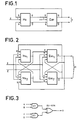
- the master elementary flip-flop marked Ma, receives a signal T at its input and it delivers on its two complementary outputs Q and to signals applied to the two inputs R and S of the slave elementary flip-flop marked Esc.
- the two outputs Q and a of the slave operator are partly looped back to the two inputs R and S of the elementary master operator Ma.
- the input R corresponds to resetting to zero (RESET in English) and input S corresponds to reset to 1 (SET in English).
- the outputs Q and to are said to be complementary. If a signal at a frequency f e is applied to the input E on the terminal T of the master operator, a signal of frequency fJ2 is available at the output of the operators.
- Figure 1 is a simplified logic diagram and each operator has two stages, each stage having a transition time tpd, so that the transition time for the master operator is 2tp d , the transition time for the slave operator is 2tp d and the maximum operating frequency of an RST flip-flop is 1 / 4tp d if it is assumed that the propagation times in the master operator and in the slave operator are the same.
- An improvement which makes it possible to double the maximum frequency of a divider, in addition to the fact that the master operator and the slave operator are identical, consists in using a timed locking of the doors, that is to say having a rocker of type RSTT, in which t is the complementary signal of the input signal T. Due to the loopback, the transition time is only 1tp d for the master operator and 1tp d for the slave operator, and the maximum operating frequency 1 / 2t pd .
- FIG. 2 represents such a flip-flop with timed locking of the doors.
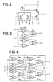
- logic function 0 A.B + C.D is achieved by integrating on a chip of fast material, single-gate, bi-gate, and shift diodes, as shown in Figure 4.
- Figure 4 is an electrical diagram of the AND / OR-NOT operator of the previous figure. It is the combination of the two operators AND of the scale which limits the operating speed of this device. These two operators which in FIG. 4 are surrounded by a dotted rectangle marked 1 are each constituted, as far as it is concerned, by a field effect transistor with two gates, each gate constituting one of the two inputs of an AND gate. .
- the frequency divider studied must work at very high frequencies such as 10 GHz, which means that the transistors are of extremely small dimensions and their gates of dimensions even smaller and therefore reach the limits of technology .
- the frequency dividers according to the prior art currently operate at maximum operating frequencies ranging from 4.1 GHz, for gate lengths of field effect transistors of 1.2 microns, up to a frequency of 5.7 GHz for gate lengths of 0.8 micron. Going beyond these frequencies therefore required a change in the design and design of the scale.
- This RST type flip-flop is made up of four OU-NON operators, 2, 3, 4, and 5 and by two OR operators, 6 and 7.
- the input signal T is applied to the two OU-NON operators 2 and 5, which also receive the R and S signals respectively.
- the two OU-NON operators 3 and 4 receive the looped 0 and Q output signals from the OR operators 6 and 7.
- FIG. 6 represents an RSTT type flip-flop. A comparison must be made between the scale of figure 2 and that of figure 6.
- the master operator Ma is made up of elementary operators 21, 31 and 61
- the master operator Ma 2 is made up of elementary operators 41, 51 and 71
- the slave complex operator Esc is made up of elementary operators 22, 32 and 62
- the slave complex operator Esc z consists of the elementary operators 42, 52 and 72.
- the flip-flop in Figure 6 is made up of the YES-NO and OR operators, according to the logic diagram in Figure 5, and this configuration makes it possible to use, in real integration on a semiconductor chip, transistors with a single grid, as shown in the wiring diagram in Figure 7.
- OR-NO operators represented by the three transistors framed by a dotted line and marked 8 and 9, and an OR operator constituted by the set of two transistors 10 and 11.
- the first interest of this kind structure is that the transistors used in the YES-NO operators, for the inputs marked A, B, C and D are single-gate transistors, that is to say it will be possible to make grids of dimensions much smaller corresponding to larger frequencies.
- the second advantage is that the OU-NON and OU functions are separate, and this advantage will be shown later.
- a divider by 2 constituted by the rocker according to figure 6 makes it possible to gain 15% in speed of operation compared to the divider using the operators AND / OR-NOT for a power dissipated equal, that is to say 20 milliwatts per operator.
- the operating frequency thus passes to 4.7 GHz, in comparison with 4.1 GHz which corresponded to a divider by 2 according to FIG. 2.
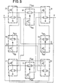
- the flip-flop in FIG. 6 comprises four stages of elementary operators, that is to say a first stage of operators OR-NO 21, 31, 41, 51, a second stage of operators OR 61, 71, a third stage of operators NO-22, 32, 42, 52, and a fourth stage of operators OR 62, 72.
- This means that the transition time through the flip-flop is equal to the sum of the transition times through each of the four stages.
- the operator OR 61 of the second stage delivers on its output a signal which is applied simultaneously to operators OR -NO 41 on the first floor and 22 on the third floor: just keep one of the two.
- the operator OR 71 of the second stage delivers on its output a signal applied simultaneously to the operators OU-NON 31 of the first stage and 52 of the third stage: the same simplification will have to be carried out.
- the OR operator 62 of the fourth stage delivers on its output a signal applied in parallel to the YES-NO operator 51 of the first stage and to the YES-NO operator 42 of the third stage.
- the OR operator 72 of the fourth stage simultaneously delivers a signal on the YES-NO operator 21 of the first stage and on the YES-NO operator 32 of the third stage.
- the divider by 2 therefore appears to be essentially constituted by two complex operators Ma, and Ma z , which control two elementary operators OR 62 and 72.
- the complex operators Ma, and Ma 2 are separated in FIG. 8 by two lines dotted lines and their designation of Ma, and Ma 2 is preserved by analogy with FIG. 6 since these complex operators consist of the same complementary operators.
- the two output OR operators are those which constitute the fourth stage of the divider by 2 in FIG. 6.
- Each of the two complex operators Ma, and Ma 2 is made up of two OR-NOT operators (21 + 31), the two outputs of which command an OR operator (61).
- the output 12 of the first ON / OFF operator (21) of the first stage controls an input of the first OR operator (62) of the third stage
- the output 13 of the second ON / OFF operator (31) of the first stage controls an input of the second OR operator (72) of the third stage.
- the output 14 of the first OR operator (61) of the second stage is looped back to an input of the third OR-NO operator (41) of the first stage.
- the interconnection diagram is symmetrical for the second complex operator Ma 2 made up of operators 41, 51, 71.
- the output 18 of the operator OR (72) of the third stage is looped back to an input of the first operator YES-NO (21) of the first stage, and the output 19 of the operator OR (62) of the third stage is looped back to an entry of the fourth operator YES-NO (51) of the first stage.
- the complex operators Ma, and Ma 2 constitute the first and second stages of the divider by 2 according to the invention.
- the outputs of the OR operators 62 and 72 deliver complementary Q and Q signals, the frequency of which is half the input frequency on the complementary inputs E and ⁇ .
- the maximum frequency of the frequency divider according to the invention is 6.25 GHz for an equivalent power per gate of 15 milliwatts, which already corresponds to an increase of 33% compared to the divider according to known art.
- the extreme performance of the divider according to the invention reaches 10 GHz: in this case, the equivalent power per gate is of 53 milliwatts.
- FIG. 9 represents the electrical diagram of the scale according to the invention and the sets of components which constitute electrical operators. are surrounded by a dotted line to facilitate their identification.
- the operators OU-NON 21, 31, 41, and 51 are in the four corners of the figure and they constitute the first stage of the divider by 2.
- the operators OR 61 and 71 are arranged on the vertical diagonal of the figure and they constitute the second stage of the divider by 2.
- the operators OR 62 and 72 are arranged on the horizontal diagonal of the figure and they constitute the third stage of the divider by 2. It can be seen that, as in FIG. 8, the inputs which deliver signals complementary T and t are addressed to the four operators of the first stage 21.
- the RST type rocker T has been developed for the production of a frequency divider by 2 characterized by a very wide operating band since its operation has been controlled between the continuous and the X band, that is to say 10 GHz .
- This circuit finds its application in the interfaces between the very high frequencies which are measured in GHz and the control or analysis systems operating at lower frequencies which are measured in MHz.
- This result was obtained by the abandonment of the flip-flop structure of the AND / OR-NOT type generally used in favor of an OR-NON / OR structure which allows technological simplification and consequently a gain in performance.
Landscapes
- Logic Circuits (AREA)
- Manipulation Of Pulses (AREA)
- Stabilization Of Oscillater, Synchronisation, Frequency Synthesizers (AREA)
Applications Claiming Priority (2)
| Application Number | Priority Date | Filing Date | Title |
|---|---|---|---|
| FR8211403 | 1982-06-29 | ||
| FR8211403A FR2529413A1 (fr) | 1982-06-29 | 1982-06-29 | Bascule logique, fonctionnant du continu a 10 ghz, et diviseur de frequence comportant cette bascule |
Publications (2)
| Publication Number | Publication Date |
|---|---|
| EP0098203A1 EP0098203A1 (fr) | 1984-01-11 |
| EP0098203B1 true EP0098203B1 (fr) | 1986-10-01 |
Family
ID=9275517
Family Applications (1)
| Application Number | Title | Priority Date | Filing Date |
|---|---|---|---|
| EP83401265A Expired EP0098203B1 (fr) | 1982-06-29 | 1983-06-17 | Bascule logique, fonctionnant du continu à 10 GHz, et diviseur de fréquence comportant cette bascule |
Country Status (5)
| Country | Link |
|---|---|
| US (1) | US4568843A (ref) |
| EP (1) | EP0098203B1 (ref) |
| JP (1) | JPS5911023A (ref) |
| DE (1) | DE3366575D1 (ref) |
| FR (1) | FR2529413A1 (ref) |
Families Citing this family (9)
| Publication number | Priority date | Publication date | Assignee | Title |
|---|---|---|---|---|
| FR2581267A1 (fr) * | 1985-04-26 | 1986-10-31 | Labo Electronique Physique | Diviseur de frequence par deux |
| US4877976A (en) * | 1987-03-13 | 1989-10-31 | Gould Inc. | Cascade FET logic circuits |
| US4939384A (en) * | 1988-10-03 | 1990-07-03 | Oki Electric Industry Co., Ltd | Flip-flop circuit |
| FR2648971B1 (fr) * | 1989-06-23 | 1991-09-06 | Thomson Composants Microondes | Circuit d'interface de sortie entre deux circuits numeriques de natures differentes |
| FR2689683B1 (fr) * | 1992-04-07 | 1994-05-20 | Thomson Composants Microondes | Dispositif semiconducteur a transistors complementaires. |
| US5633607A (en) * | 1995-04-28 | 1997-05-27 | Mosaid Technologies Incorporated | Edge triggered set-reset flip-flop (SRFF) |
| DE10320793B4 (de) * | 2003-04-30 | 2005-04-21 | Infineon Technologies Ag | Schaltungs-Einrichtung, insbesondere Latch- oder Phasen-Detektor-Einrichtung |
| EP1678829B1 (en) * | 2003-10-23 | 2010-04-21 | Nxp B.V. | Frequency divider |
| KR102230370B1 (ko) * | 2014-08-06 | 2021-03-23 | 엘지디스플레이 주식회사 | 표시장치 |
Family Cites Families (2)
| Publication number | Priority date | Publication date | Assignee | Title |
|---|---|---|---|---|
| US3845325A (en) * | 1973-04-23 | 1974-10-29 | Motorola Inc | Igfet flip-flop having facility for forcing its state |
| FR2362534A1 (fr) * | 1976-04-01 | 1978-03-17 | Labo Electronique Physique | Circuit diviseur logique |
-
1982
- 1982-06-29 FR FR8211403A patent/FR2529413A1/fr active Granted
-
1983
- 1983-06-17 EP EP83401265A patent/EP0098203B1/fr not_active Expired
- 1983-06-17 US US06/505,175 patent/US4568843A/en not_active Expired - Fee Related
- 1983-06-17 DE DE8383401265T patent/DE3366575D1/de not_active Expired
- 1983-06-28 JP JP58116833A patent/JPS5911023A/ja active Granted
Non-Patent Citations (2)
| Title |
|---|
| ELECTRONICS LETTERS, vol. 16, no. 14, 3 juillet 1980, pages 535-536, Hitchin, Herts., GB. M. CHATHELIN et al.: "5 GHz binary frequency division on GaAs" * |
| IEEE INTERNATIONAL SOLID STATE CIRCUITS CONFERENCE, vol. 20, no. 20, 18 février 1977, pages 198-199, IEEE, New York, USA. R. VAN TUYL et al.: "4-GHz frequency division with GaAs MESFETICs" * |
Also Published As
| Publication number | Publication date |
|---|---|
| DE3366575D1 (en) | 1986-11-06 |
| US4568843A (en) | 1986-02-04 |
| FR2529413B1 (ref) | 1985-02-08 |
| FR2529413A1 (fr) | 1983-12-30 |
| JPS5911023A (ja) | 1984-01-20 |
| EP0098203A1 (fr) | 1984-01-11 |
| JPH0430762B2 (ref) | 1992-05-22 |
Similar Documents
| Publication | Publication Date | Title |
|---|---|---|
| EP0098203B1 (fr) | Bascule logique, fonctionnant du continu à 10 GHz, et diviseur de fréquence comportant cette bascule | |
| CA2137340C (fr) | Arbre de portes logique ou - exclusif et multiplieur de frequence l'incorporant | |
| FR2640829A1 (fr) | Dispositif pour la modulation ou la demodulation directe en hyperfrequences | |
| EP0872959B1 (fr) | Diviseur de fréquence à faible bruit. | |
| EP0130645B1 (fr) | Diviseur de fréquence par deux | |
| FR2597262A1 (fr) | Circuit integre a semi-conducteur avec condensateur de derivation associe a son cablage | |
| EP0487386B1 (fr) | Dispositif doubleur de fréquence | |
| FR3143238A1 (fr) | Polarisation adaptative de substrat utilisant des détecteurs de marge | |
| EP0237094A1 (fr) | Dispositif semi-conducteur du type réseau de portes prédiffusé pour circuits à la demande | |
| EP0120744B1 (fr) | Diviseur de fréquence par deux, analogique et apériodique | |
| FR3034930B1 (fr) | Procede et dispositif d'auto-calibration de circuits multi-grilles | |
| EP1081848B1 (fr) | Dispositif de transposition de fréquence à faible fuite de signal d'oscillateur local et procédé correspondant de réduction de fuite | |
| FR2719728A1 (fr) | Diviseur de fréquence, synthétiseur de fréquence comportant un tel diviseur et radiotéléphone comportant un tel synthétiseur. | |
| EP3627707A1 (fr) | Dispositif de synthèse de fréquence à rang de multiplication élevé | |
| FR2648643A1 (fr) | Circuit d'interface entre deux circuits numeriques de natures differentes | |
| EP0928060A1 (fr) | Convertisseur de tension continue à rendement amélioré | |
| CA2146196A1 (fr) | Circuit a retard reglable | |
| EP0981203B1 (fr) | Source de courant contrôlée à commutation accélérée | |
| EP1113579A1 (fr) | Procédé pour diviser la fréquence d'un signal | |
| EP0277665B1 (fr) | Circuit réalisant la fonction OU-EXCLUSIF | |
| EP0424222A1 (fr) | Circuit intégré logique, à temps de basculement réglable | |
| FR2573939A1 (fr) | Circuit multiplexeur de signaux integre a quatre voies d'entree | |
| EP0218508A1 (fr) | Générateur de fréquences à variation rapide | |
| EP0073870B1 (fr) | Multivibrateur monostable intégré sans condensateur | |
| FR2909238A1 (fr) | Mixeur et procede de traitement de signaux, systeme sur puce comprenant un tel mixeur |
Legal Events
| Date | Code | Title | Description |
|---|---|---|---|
| PUAI | Public reference made under article 153(3) epc to a published international application that has entered the european phase |
Free format text: ORIGINAL CODE: 0009012 |
|
| AK | Designated contracting states |
Designated state(s): DE GB IT NL |
|
| 17P | Request for examination filed |
Effective date: 19840120 |
|
| GRAA | (expected) grant |
Free format text: ORIGINAL CODE: 0009210 |
|
| AK | Designated contracting states |
Kind code of ref document: B1 Designated state(s): DE GB IT NL |
|
| ITF | It: translation for a ep patent filed | ||
| REF | Corresponds to: |
Ref document number: 3366575 Country of ref document: DE Date of ref document: 19861106 |
|
| PLBE | No opposition filed within time limit |
Free format text: ORIGINAL CODE: 0009261 |
|
| STAA | Information on the status of an ep patent application or granted ep patent |
Free format text: STATUS: NO OPPOSITION FILED WITHIN TIME LIMIT |
|
| 26N | No opposition filed | ||
| ITTA | It: last paid annual fee | ||
| PGFP | Annual fee paid to national office [announced via postgrant information from national office to epo] |
Ref country code: NL Payment date: 19950519 Year of fee payment: 13 |
|
| PGFP | Annual fee paid to national office [announced via postgrant information from national office to epo] |
Ref country code: DE Payment date: 19950520 Year of fee payment: 13 |
|
| PGFP | Annual fee paid to national office [announced via postgrant information from national office to epo] |
Ref country code: GB Payment date: 19950524 Year of fee payment: 13 |
|
| PG25 | Lapsed in a contracting state [announced via postgrant information from national office to epo] |
Ref country code: GB Effective date: 19960617 |
|
| PG25 | Lapsed in a contracting state [announced via postgrant information from national office to epo] |
Ref country code: NL Effective date: 19970101 |
|
| GBPC | Gb: european patent ceased through non-payment of renewal fee |
Effective date: 19960617 |
|
| PG25 | Lapsed in a contracting state [announced via postgrant information from national office to epo] |
Ref country code: DE Effective date: 19970301 |
|
| NLV4 | Nl: lapsed or anulled due to non-payment of the annual fee |
Effective date: 19970101 |