EP0097789B1 - Method of filling trenches in semiconductor substrates with silicon - Google Patents
Method of filling trenches in semiconductor substrates with silicon Download PDFInfo
- Publication number
- EP0097789B1 EP0097789B1 EP83104287A EP83104287A EP0097789B1 EP 0097789 B1 EP0097789 B1 EP 0097789B1 EP 83104287 A EP83104287 A EP 83104287A EP 83104287 A EP83104287 A EP 83104287A EP 0097789 B1 EP0097789 B1 EP 0097789B1
- Authority
- EP
- European Patent Office
- Prior art keywords
- trench
- silicon
- nucleating material
- sidewalls
- nucleating
- Prior art date
- Legal status (The legal status is an assumption and is not a legal conclusion. Google has not performed a legal analysis and makes no representation as to the accuracy of the status listed.)
- Expired
Links
Images

Classifications
-
- H—ELECTRICITY
- H01—ELECTRIC ELEMENTS
- H01L—SEMICONDUCTOR DEVICES NOT COVERED BY CLASS H10
- H01L21/00—Processes or apparatus adapted for the manufacture or treatment of semiconductor or solid state devices or of parts thereof
- H01L21/70—Manufacture or treatment of devices consisting of a plurality of solid state components formed in or on a common substrate or of parts thereof; Manufacture of integrated circuit devices or of parts thereof
- H01L21/71—Manufacture of specific parts of devices defined in group H01L21/70
- H01L21/76—Making of isolation regions between components
- H01L21/763—Polycrystalline semiconductor regions
-
- H—ELECTRICITY
- H01—ELECTRIC ELEMENTS
- H01L—SEMICONDUCTOR DEVICES NOT COVERED BY CLASS H10
- H01L21/00—Processes or apparatus adapted for the manufacture or treatment of semiconductor or solid state devices or of parts thereof
- H01L21/02—Manufacture or treatment of semiconductor devices or of parts thereof
- H01L21/02104—Forming layers
- H01L21/02365—Forming inorganic semiconducting materials on a substrate
- H01L21/02367—Substrates
- H01L21/0237—Materials
- H01L21/02373—Group 14 semiconducting materials
- H01L21/02381—Silicon, silicon germanium, germanium
-
- H—ELECTRICITY
- H01—ELECTRIC ELEMENTS
- H01L—SEMICONDUCTOR DEVICES NOT COVERED BY CLASS H10
- H01L21/00—Processes or apparatus adapted for the manufacture or treatment of semiconductor or solid state devices or of parts thereof
- H01L21/02—Manufacture or treatment of semiconductor devices or of parts thereof
- H01L21/02104—Forming layers
- H01L21/02365—Forming inorganic semiconducting materials on a substrate
- H01L21/02518—Deposited layers
- H01L21/02521—Materials
- H01L21/02524—Group 14 semiconducting materials
- H01L21/02532—Silicon, silicon germanium, germanium
-
- H—ELECTRICITY
- H01—ELECTRIC ELEMENTS
- H01L—SEMICONDUCTOR DEVICES NOT COVERED BY CLASS H10
- H01L21/00—Processes or apparatus adapted for the manufacture or treatment of semiconductor or solid state devices or of parts thereof
- H01L21/02—Manufacture or treatment of semiconductor devices or of parts thereof
- H01L21/02104—Forming layers
- H01L21/02365—Forming inorganic semiconducting materials on a substrate
- H01L21/02612—Formation types
- H01L21/02617—Deposition types
- H01L21/0262—Reduction or decomposition of gaseous compounds, e.g. CVD
-
- H—ELECTRICITY
- H01—ELECTRIC ELEMENTS
- H01L—SEMICONDUCTOR DEVICES NOT COVERED BY CLASS H10
- H01L21/00—Processes or apparatus adapted for the manufacture or treatment of semiconductor or solid state devices or of parts thereof
- H01L21/02—Manufacture or treatment of semiconductor devices or of parts thereof
- H01L21/02104—Forming layers
- H01L21/02365—Forming inorganic semiconducting materials on a substrate
- H01L21/02612—Formation types
- H01L21/02617—Deposition types
- H01L21/02636—Selective deposition, e.g. simultaneous growth of mono- and non-monocrystalline semiconductor materials
- H01L21/02639—Preparation of substrate for selective deposition
-
- H—ELECTRICITY
- H01—ELECTRIC ELEMENTS
- H01L—SEMICONDUCTOR DEVICES NOT COVERED BY CLASS H10
- H01L21/00—Processes or apparatus adapted for the manufacture or treatment of semiconductor or solid state devices or of parts thereof
- H01L21/70—Manufacture or treatment of devices consisting of a plurality of solid state components formed in or on a common substrate or of parts thereof; Manufacture of integrated circuit devices or of parts thereof
- H01L21/71—Manufacture of specific parts of devices defined in group H01L21/70
- H01L21/74—Making of localized buried regions, e.g. buried collector layers, internal connections substrate contacts
- H01L21/743—Making of internal connections, substrate contacts
Definitions
- This invention relates to a method of filling trenches in semiconductor substrates with polycrystalline silicon or epitaxial silicon or both.
- the method of the present invention is particularly applicable to the filling of trenches employed for device isolation purposes.
- deep trenches can be formed according to the procedures disclosed in U.S.-A-4,256,514.
- the refill techniques employed in deep trench formations have been chemical vapor deposition (CVD) systems.
- CVD chemical vapor deposition
- Such systems involve a homogeneous gas phase reaction.
- that process suffers from a serious reliability problem in that there is a tendency to form large voids within the trench.
- voids are formed at the bottom of the trenches and/or large continuous openings are formed extending to the final surface after subsequent planarization.
- the refill deposited by such procedure can be structurally deficient (e.g., loosely packed) which can lead to problems in future processing.
- the presence of voids has a tendency to magnify the formation of defects in silicon areas later to serve as active or device regions. This is particularly so if the formation continues up to the surface followed by subsequent oxidation or isolation.
- substrate surfaces which are relatively densely populated with trenches in some areas and less densely populated in others have been found to display local deposition thickness variations. This is due to depletion effects arising from the presence of increased area. These overall surface variations can cause problems in later planarization steps.
- Patent Abstracts of Japan, Volume 6, Number 37 (E-97) [915], 6th March 1982 discloses a method of filling a vertically sided trench let into a surface of a silicon substrate with silicon, comprising the steps of covering the silicon surface into which the trench is let and the base and both sidewalls of the trench with non-nucleating material, providing a layer of polycrystalline silicon as nucleating material on the base, but not the sidewalls, of the trench and growing silicon perpendicularly from the base of the trench.
- EP-A-0 023 146 discloses a method of forming an isolation region in the manufacture of a semiconductor device in which a groove in a semiconductor substrate is filled with polycrystalline silicon, a layer of resinous material deposited over the filled substrate to provide a flat surface and the structure etched back to provide a flat surface on which the polycrystalline silicon is exposed.
- the present invention makes it possible to significantly reduce, if not entirely eliminate, the problem of void formation in isolation trenches experienced by prior techniques.
- the present invention provides a method of filling a trench let into a surface of a semiconductor substrate with silicon, comprising the steps of: covering the semiconductor surface into which the trench is let and either the base or the sidewalls but not both the base and the sidewalls of the trench with non-nucleating material, providing a layer of nucleating material on at least a portion of the surface of the non-nucleating material and growing silicon perpendicularly from the base or sidewalls of the trench.
- the substrate 1 can be a P-type silicon substrate having any desired crystal orientation (e.g. ⁇ 100>).
- a substrate can be prepared by slicing and polishing a P-type silicon boule grown in the presence of a P-type dopant, such as boron, following conventional crystal growth techniques.
- P-type dopants for silicon include aluminium, gallium, and indium.
- Each of the deep trenches 2 has a substantially horizontal surface 3 and substantially vertical surfaces 4. Generally, the surfaces 4 are vertical or less than about 5° from the vertical.
- the trenches can be formed by the process disclosed in U.S.-A-4,256,514. Generally, the ratio of the depth of the trench to the width of the trench is between about 3.5 to 1 and 2.5 to 1. Of course, larger ratios such as about 4 to 1 are within the scope of the present invention. Typically, the depth of the trench is about 3.5 to 4 pm and the width is about 1 to 2.5 pm.
- n+ regions 5 Adjacent the lower portion of the trenches 2 are n+ regions 5 and adjacent the upper portion of the trenches are n regions 6. Such regions are desirably formed by ion implantation or thermal diffusion either before or after the formation of the trenches 2.
- layer 7 is also grown along the horizontal surface 3 of trench 2.
- the non-nucleating layer is a relatively thin layer about 0.2 pm to about 0.5 pm thick and typically about 0.3 11m thick.
- the non-nucleating layer can be provided by any well-known method, such as by thermal oxidation.
- the thickness of the non-nucleating layer on surface 3 need not be the same as the thickness of the non-nucleating layer on surfaces 4.
- the non-nucleating layer 7 is provided on at least one of the surfaces located along the longest axis of the trench. In the structure shown in Figure 1, the longest axis is along the vertical walls 4 of the trench.
- a layer 8 of nucleating material is formed on at least one of the surfaces of the non-nucleating layer 7 as shown in Figure 2.
- this layer is about 50 nm to about 300 nm thick. It has been noted that if the nucleating layer is too thin, or less than about 50 nm, then back etching can occur during the filling technique which thereby causes void formation and decreased speed in the filling technique.
- the nucleating layer can be deposited by either atmospheric or a low pressure CVD technique to provide polycrystalline silicon. It is preferred that the relatively thin nucleating layer be deposited by low temperature techniques, using temperatures up to about 650°C.
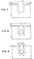
- Figure 2 illustrates a preferred configuration wherein the nucleating layer 8 is present only on the horizontal surface 3 of the trench and on the horizontal surfaces of the non-nucleating layer on top of the silicon substrate.
- Figure 7 shows the nucleating layer 8 on top of the non-nucleating material 7 on the horizontal surface of the substrate located outside trench 2.
- the bottom 3 of trench 2 is exposed silicon which also acts as a nucleating material.
- Non-nucleating material 7 is present on the vertical walls of the trench.
- Figure 8 illustrates covering the non-nucleating material 7 on the vertical walls 4 of the trench and the horizontal layer outside the trench with a nucleating layer.
- the horizontal surface 3 of trench 2 is exposed substrate 1.
- Figure 9 illustrates providing nucleating material 8 on the non-nucleating material 7 on the vertical sidewalls 4 of trench 2.
- the horizontal bottom portion 3 of trench 2 is exposed silicon.
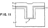
- Figure 11 illustrates providing a nucleating layer 8 over all of the surfaces of trench 2 wherein the horizontal surface 3 of trench 2 is exposed silicon substrate and the vertical surfaces 4 of trench 2 are non-nucleating material 7.
- the techniques illustrated in Figures 8-11 are not particularly preferred since small amounts of voids have been noted in their formation.
- the nucleating material within the trench be present on either only the vertical surfaces 4 or only on the horizontal surface 3.
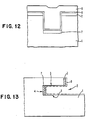
- Figure 12 Illustrates providing a non-nucleating material layer 7 on the horizontal surface of trench 2 and on the horizontal surfaces located outside trench 2.
- the nucleating layer 8 is provided over all surfaces of the trench (ie vertical walls 4, horizontal surface 3) and on the horizontal surface above the non-nucleating layer 7 on the substrate located outside trench 2.
- Figure 13 illustrates a structure wherein the trench is about 90° from that shown in Figure 12.
- Figure 13 illustrates providing a non-nucleating material layer 7 on the vertical surface of the trench 2.
- the nucleating layer 8 is provided over all surfaces of the trench and on the vertical surfaces outside the trench.
- the preferred nucleating layer is polycrystalline silicon.
- silicon 9 is grown in trench 2 and on all surfaces containing the nucleating material.
- the preferred method of growing the silicon according to the present invention is by a gas-solid or heterogeneous reaction system.
- the growth occurs perpendicularly from the nucleating surfaces.
- the heterogeneous reaction system desirably includes hydrogen, silicon, and chlorine.
- a particularly preferred system is a combination of SiCl 4 -H Z as discussed by Silvestri and Tang-Reproducible Technique for Simultaneous Deposition of Poly-Epi on Oxide-Silicon, IBM Technical Disclosure Bulletin, Volume 23, No. 2, July 1980 pages, 819 and 820.
- the filling process is generally carried out at temperatures between about 900 and about 1100°C and preferably about 1000°C to provide a sufficiently fast filling of the trenches. It is important that the filling of the trenches is completed in about 20 minutes or less so that the dopant impurities already present in the substrate are not disturbed due to the exposure to elevated temperatures. With the typical dimensions discussed hereinabove, the filling rate to provide a practical process is at least about 0.22 pm per minute.
- silicon fill that will be present within the trenches will depend upon the type of nucleating surface present. For instance, polycrystalline nucleating surfaces will result in the formation of polycrystalline silicon. On the other hand, silicon nucleating surfaces, such as shown in Figures 7, 8, and 9 will result in epitaxial silicon growth. Accordingly, as illustrated in Figures 7, 8, and 9 there will be a combination of polycrystalline silicon 9A and epitaxial silicon 9B.
- the silicon layer 9 is planarized for example by a technique discussed in U.S.-A-4,256,514 employing either CI/argon or CBrF 3 .
- the preferred technique comprises providing a relatively thick layer of resist material 10 over the grown silicon surfaces as illustrated in Figure 4.
- the photoresist material can be applied by well-known techniques such as spinning on or by spraying.
- the photoresist material tends to flow and provide a substantially level surface as indicated in Figure 4.
- the particular photoresist material employed for this purpose is not critical and any type, negative or positive, of photoresist material can be employed. This is possible since the subsequent steps, as will be discussed hereinbelow, are not dependent upon the chemical identity of the photoresist material.
- Suitable photoresist materials include compositions based on phenolformaldehyde novalak polymers.
- Shipley 1350 which is an m-cresol formaldehyde novalak polymer composition.
- This is a positive resist composition and includes therein a diazoketone, such as 2-diazo-1-naphthol-5-sulphonic acid ester.
- the composition usually contains about 15% by weight of the diazoketone compound.
- the diazoketone is attached directly to the polymer molecules.
- a discussion of photoresist materials can be found, for instance, in Journal of the Electrochemical Society, Vol 125, No. 3, March 1980-Deckert et al, "Micro-lithography-Key to Solid-State Fabrication", pp 45C to 56C.
- the photoresist is generally applied in a thickness of about 2 to about 4 pm.
- the reactive ion etching procedure employs conditions such that polycrystalline silicon and/ or epitaxial silicon etches at the same rate as the photoresist material and at a rate substantially higher than silicon dioxide.
- the relative amount of the reactive gases, in particular CF 4 and 0 2 , and the pressure and the rf power to the two electrodes are adjusted such that the etch rate of the photoresist material is about equal to that of the epitaxial silicon.
- a particularly preferred system contains about 20% by volume of 0 2 at a pressure of about 100 millitorr (13.3 N/m 2 ).
- the rf power density to the substrate electrode is 0.27W/cm 2 and the rf power density to the substrate electrode is 0.lW/ CM 2 .
- the flow rate of the etching gas is about 40 SCCM and the temperature of the wafer is between 60 and 100°C. Under these conditions, the etch rate of silicon and photoresist is about 60 nm/min and the etch rate of Si0 2 is 7.0 nm/min. Thus, etching stops at the oxide surface 7.
- the silicon is etched a small distance inside the trench 2, such as about 200 nm.
- the particular devices can be fabricated on and in the substrate.
- the surfaces of the remaining polycrystalline silicon 9 in the trench can be doped to provide an n+ region, for example, by being doped with POCI 3 .
- the polycrystalline silicon can now be oxidized to provide isolation regions 11 on top of the n+ regions. It is noted that the polycrystalline silicon, since it is heavily doped, is oxidized about 4 times as fast as oxidation growth on the epitaxial silicon at a temperature of about 800°C. Accordingly, subsequent to the oxide growth, the oxide can be etched to leave oxide remaining on the polycrystalline silicon, but exposing the epitaxial silicon region.
Landscapes
- Engineering & Computer Science (AREA)
- Physics & Mathematics (AREA)
- Condensed Matter Physics & Semiconductors (AREA)
- General Physics & Mathematics (AREA)
- Manufacturing & Machinery (AREA)
- Computer Hardware Design (AREA)
- Microelectronics & Electronic Packaging (AREA)
- Power Engineering (AREA)
- Chemical & Material Sciences (AREA)
- Crystallography & Structural Chemistry (AREA)
- Materials Engineering (AREA)
- Element Separation (AREA)
Description
- This invention relates to a method of filling trenches in semiconductor substrates with polycrystalline silicon or epitaxial silicon or both. The method of the present invention is particularly applicable to the filling of trenches employed for device isolation purposes.
- It has been suggested to form relatively deep trenches in semiconductor substrates and then to refill the trenches in order to provide isolation between active regions or devices in the substrate. For instance, deep trenches can be formed according to the procedures disclosed in U.S.-A-4,256,514. The refill techniques employed in deep trench formations have been chemical vapor deposition (CVD) systems. Such systems involve a homogeneous gas phase reaction. The silicon dioxide or polycrystalline silicon formed in the gas from the reactive gas species present, essentially "drops" onto surfaces and into the trench structures. However, that process suffers from a serious reliability problem in that there is a tendency to form large voids within the trench. In fact, frequently voids are formed at the bottom of the trenches and/or large continuous openings are formed extending to the final surface after subsequent planarization. Moreover, the refill deposited by such procedure can be structurally deficient (e.g., loosely packed) which can lead to problems in future processing. The presence of voids has a tendency to magnify the formation of defects in silicon areas later to serve as active or device regions. This is particularly so if the formation continues up to the surface followed by subsequent oxidation or isolation. Moreover, substrate surfaces which are relatively densely populated with trenches in some areas and less densely populated in others have been found to display local deposition thickness variations. This is due to depletion effects arising from the presence of increased area. These overall surface variations can cause problems in later planarization steps.
- Patent Abstracts of Japan,
Volume 6, Number 37 (E-97) [915], 6th March 1982 discloses a method of filling a vertically sided trench let into a surface of a silicon substrate with silicon, comprising the steps of covering the silicon surface into which the trench is let and the base and both sidewalls of the trench with non-nucleating material, providing a layer of polycrystalline silicon as nucleating material on the base, but not the sidewalls, of the trench and growing silicon perpendicularly from the base of the trench. - EP-A-0 023 146 discloses a method of forming an isolation region in the manufacture of a semiconductor device in which a groove in a semiconductor substrate is filled with polycrystalline silicon, a layer of resinous material deposited over the filled substrate to provide a flat surface and the structure etched back to provide a flat surface on which the polycrystalline silicon is exposed.
- The present invention makes it possible to significantly reduce, if not entirely eliminate, the problem of void formation in isolation trenches experienced by prior techniques.
- The present invention provides a method of filling a trench let into a surface of a semiconductor substrate with silicon, comprising the steps of: covering the semiconductor surface into which the trench is let and either the base or the sidewalls but not both the base and the sidewalls of the trench with non-nucleating material, providing a layer of nucleating material on at least a portion of the surface of the non-nucleating material and growing silicon perpendicularly from the base or sidewalls of the trench.
- How the invention can be carried out will now be described by way of example, with reference to the accompanying drawings, in which:-
- Figures 1-6 are cross-sectional views of a substrate at successive stages of processing demonstrating a basic method; and
- Figures 7-13 are cross-sectional views of representative substrates containing a nucleating layer on various alternative surfaces suitable for carrying out the present invention.
- For convenience, the discussion of the process steps is directed to employing a P-type silicon substrate as the semiconductor substrate and N-type impurities as the dopant impurities. Of course, as an alternative, an N-type substrate and P-type dopant impurities can be employed. References to horizontal and/or vertical surfaces or walls are relative to the major surfaces of the substrate.
- When the discussion refers to N-type impurities, the process steps are applicable to P-type impurities and vice versa. Also, the present invention is applicable to substrates other than silicon. Moreover, the terms "polysilicon" and polycrystalline silicon are used herein interchangeably as in the prior art.
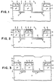
- Referring to Figure 1, there is shown a fragment of a semiconductor substrate 1 having trenches 2 therein. The substrate 1 can be a P-type silicon substrate having any desired crystal orientation (e.g. <100>). Such a substrate can be prepared by slicing and polishing a P-type silicon boule grown in the presence of a P-type dopant, such as boron, following conventional crystal growth techniques. Other P-type dopants for silicon include aluminium, gallium, and indium.
- Each of the deep trenches 2 has a substantially
horizontal surface 3 and substantiallyvertical surfaces 4. Generally, thesurfaces 4 are vertical or less than about 5° from the vertical. The trenches can be formed by the process disclosed in U.S.-A-4,256,514. Generally, the ratio of the depth of the trench to the width of the trench is between about 3.5 to 1 and 2.5 to 1. Of course, larger ratios such as about 4 to 1 are within the scope of the present invention. Typically, the depth of the trench is about 3.5 to 4 pm and the width is about 1 to 2.5 pm. - Adjacent the lower portion of the trenches 2 are
n+ regions 5 and adjacent the upper portion of the trenches are nregions 6. Such regions are desirably formed by ion implantation or thermal diffusion either before or after the formation of the trenches 2. - A non-nucleating
layer 7, such as silicon dioxide, silicon nitride, aluminium oxide, or mixtures thereof, is grown on at least one of the surfaces within trench 2 such as on thevertical surfaces 4 within trench 2. For convenience,layer 7 is also grown along thehorizontal surface 3 of trench 2. The non-nucleating layer is a relatively thin layer about 0.2 pm to about 0.5 pm thick and typically about 0.3 11m thick. The non-nucleating layer can be provided by any well-known method, such as by thermal oxidation. In addition, the thickness of the non-nucleating layer onsurface 3 need not be the same as the thickness of the non-nucleating layer onsurfaces 4. Preferably thenon-nucleating layer 7 is provided on at least one of the surfaces located along the longest axis of the trench. In the structure shown in Figure 1, the longest axis is along thevertical walls 4 of the trench. - Next, a
layer 8 of nucleating material is formed on at least one of the surfaces of thenon-nucleating layer 7 as shown in Figure 2. Typically, this layer is about 50 nm to about 300 nm thick. It has been noted that if the nucleating layer is too thin, or less than about 50 nm, then back etching can occur during the filling technique which thereby causes void formation and decreased speed in the filling technique. The nucleating layer can be deposited by either atmospheric or a low pressure CVD technique to provide polycrystalline silicon. It is preferred that the relatively thin nucleating layer be deposited by low temperature techniques, using temperatures up to about 650°C. Figure 2 illustrates a preferred configuration wherein thenucleating layer 8 is present only on thehorizontal surface 3 of the trench and on the horizontal surfaces of the non-nucleating layer on top of the silicon substrate. - Configurations of the nucleating layer within the scope of the present invention are shown in Figures 7 through 13. For instance, Figure 7 shows the
nucleating layer 8 on top of thenon-nucleating material 7 on the horizontal surface of the substrate located outside trench 2. Thebottom 3 of trench 2 is exposed silicon which also acts as a nucleating material. Non-nucleatingmaterial 7 is present on the vertical walls of the trench. Figure 8 illustrates covering thenon-nucleating material 7 on thevertical walls 4 of the trench and the horizontal layer outside the trench with a nucleating layer. Thehorizontal surface 3 of trench 2 is exposed substrate 1. Figure 9 illustrates providingnucleating material 8 on the non-nucleatingmaterial 7 on thevertical sidewalls 4 of trench 2. Thehorizontal bottom portion 3 of trench 2 is exposed silicon. Figure 11 illustrates providing anucleating layer 8 over all of the surfaces of trench 2 wherein thehorizontal surface 3 of trench 2 is exposed silicon substrate and thevertical surfaces 4 of trench 2 arenon-nucleating material 7. The techniques illustrated in Figures 8-11 are not particularly preferred since small amounts of voids have been noted in their formation. - Accordingly, it is preferred that the nucleating material within the trench be present on either only the
vertical surfaces 4 or only on thehorizontal surface 3. - Figure 12'illustrates providing a
non-nucleating material layer 7 on the horizontal surface of trench 2 and on the horizontal surfaces located outside trench 2. Thenucleating layer 8 is provided over all surfaces of the trench (ievertical walls 4, horizontal surface 3) and on the horizontal surface above the non-nucleatinglayer 7 on the substrate located outside trench 2. - The present invention is also applicable to filling trenches which are located substantially parallel to or at any angle to the top surface of the substrate in addition to the trenches shown which are substantially perpendicular to the top surface of the substrate. For example, Figure 13 illustrates a structure wherein the trench is about 90° from that shown in Figure 12. In particular, Figure 13 illustrates providing a
non-nucleating material layer 7 on the vertical surface of the trench 2. Thenucleating layer 8 is provided over all surfaces of the trench and on the vertical surfaces outside the trench. The preferred nucleating layer is polycrystalline silicon. - Next,
silicon 9 is grown in trench 2 and on all surfaces containing the nucleating material. The preferred method of growing the silicon according to the present invention is by a gas-solid or heterogeneous reaction system. In particular, the growth occurs perpendicularly from the nucleating surfaces. The heterogeneous reaction system desirably includes hydrogen, silicon, and chlorine. A particularly preferred system is a combination of SiCl4-HZ as discussed by Silvestri and Tang-Reproducible Technique for Simultaneous Deposition of Poly-Epi on Oxide-Silicon, IBM Technical Disclosure Bulletin, Volume 23, No. 2, July 1980 pages, 819 and 820. - The problem addressed by the present invention of preventing void formation in deep trenches was not encountered in the process discussed by Silvestri and Tang in their publication because the latter is not concerned with deep trench filling.
- The filling process is generally carried out at temperatures between about 900 and about 1100°C and preferably about 1000°C to provide a sufficiently fast filling of the trenches. It is important that the filling of the trenches is completed in about 20 minutes or less so that the dopant impurities already present in the substrate are not disturbed due to the exposure to elevated temperatures. With the typical dimensions discussed hereinabove, the filling rate to provide a practical process is at least about 0.22 pm per minute.
- In addition to the ability to achieve a void-free fill, the technique employed also improves the planarity of the surfaces as discussed in the aforementioned IBM Technical Disclosure Bulletin.
- The type of silicon fill that will be present within the trenches will depend upon the type of nucleating surface present. For instance, polycrystalline nucleating surfaces will result in the formation of polycrystalline silicon. On the other hand, silicon nucleating surfaces, such as shown in Figures 7, 8, and 9 will result in epitaxial silicon growth. Accordingly, as illustrated in Figures 7, 8, and 9 there will be a combination of
polycrystalline silicon 9A andepitaxial silicon 9B. - It has been noted that the silicon in the above types of systems grow faster within holes than on adjacent flat surfaces on single crystal surfaces. Along these lines, see Runyan et al, Journal Electro-Chemical Society, Behavior of Large-Scale Surface Perturbations During Silicon Epitaxial Growth, November 1967, pages 1154-1157. This phenomenon may be due to the existence of higher temperatures at the bottom of the hole and the lack of carrier gas flow in the holes. In addition, in view of the fact that the growth in the trench is faster than on the adjacent flat surfaces, the surface topology is improved.
- Next, the
silicon layer 9 is planarized for example by a technique discussed in U.S.-A-4,256,514 employing either CI/argon or CBrF3. However, the preferred technique comprises providing a relatively thick layer of resistmaterial 10 over the grown silicon surfaces as illustrated in Figure 4. The photoresist material can be applied by well-known techniques such as spinning on or by spraying. The photoresist material tends to flow and provide a substantially level surface as indicated in Figure 4. The particular photoresist material employed for this purpose is not critical and any type, negative or positive, of photoresist material can be employed. This is possible since the subsequent steps, as will be discussed hereinbelow, are not dependent upon the chemical identity of the photoresist material. Examples of suitable photoresist materials include compositions based on phenolformaldehyde novalak polymers. A particular example of such is Shipley 1350 which is an m-cresol formaldehyde novalak polymer composition. This is a positive resist composition and includes therein a diazoketone, such as 2-diazo-1-naphthol-5-sulphonic acid ester. The composition usually contains about 15% by weight of the diazoketone compound. In addition, in other systems, the diazoketone is attached directly to the polymer molecules. A discussion of photoresist materials can be found, for instance, in Journal of the Electrochemical Society, Vol 125, No. 3, March 1980-Deckert et al, "Micro-lithography-Key to Solid-State Fabrication", pp 45C to 56C. The photoresist is generally applied in a thickness of about 2 to about 4 pm. - Next, the structure is subjected to reactive ion etching. The apparatus disclosed in Ephrath, IEEE Transactions on Electron Devices, Reactive Ion Etching for VLSI, Vol, ED-28, No. 11, November 1981, p 1315 to 1319 and Ephrath, Semiconductor Silicon 1981, The Electrochemical Society, Dry Etching for VLSI-A Review pp 627 to 637, can be employed for this purpose.
- The reactive ion etching procedure employs conditions such that polycrystalline silicon and/ or epitaxial silicon etches at the same rate as the photoresist material and at a rate substantially higher than silicon dioxide. The relative amount of the reactive gases, in particular CF4 and 02, and the pressure and the rf power to the two electrodes are adjusted such that the etch rate of the photoresist material is about equal to that of the epitaxial silicon. A particularly preferred system contains about 20% by volume of 02 at a pressure of about 100 millitorr (13.3 N/m2). The rf power density to the substrate electrode is 0.27W/cm2 and the rf power density to the substrate electrode is 0.lW/CM2 . The flow rate of the etching gas is about 40 SCCM and the temperature of the wafer is between 60 and 100°C. Under these conditions, the etch rate of silicon and photoresist is about 60 nm/min and the etch rate of Si02 is 7.0 nm/min. Thus, etching stops at the
oxide surface 7. - If desired, as illustrated in Figure 5, the silicon is etched a small distance inside the trench 2, such as about 200 nm.
- Next, the particular devices can be fabricated on and in the substrate. For instance, as an example, the surfaces of the remaining
polycrystalline silicon 9 in the trench can be doped to provide an n+ region, for example, by being doped with POCI3. If desired, the polycrystalline silicon can now be oxidized to provideisolation regions 11 on top of the n+ regions. It is noted that the polycrystalline silicon, since it is heavily doped, is oxidized about 4 times as fast as oxidation growth on the epitaxial silicon at a temperature of about 800°C. Accordingly, subsequent to the oxide growth, the oxide can be etched to leave oxide remaining on the polycrystalline silicon, but exposing the epitaxial silicon region.
Claims (20)
Applications Claiming Priority (2)
| Application Number | Priority Date | Filing Date | Title |
|---|---|---|---|
| US06/393,997 US4473598A (en) | 1982-06-30 | 1982-06-30 | Method of filling trenches with silicon and structures |
| US393997 | 1982-06-30 |
Publications (3)
| Publication Number | Publication Date |
|---|---|
| EP0097789A2 EP0097789A2 (en) | 1984-01-11 |
| EP0097789A3 EP0097789A3 (en) | 1986-08-20 |
| EP0097789B1 true EP0097789B1 (en) | 1990-04-11 |
Family
ID=23557108
Family Applications (1)
| Application Number | Title | Priority Date | Filing Date |
|---|---|---|---|
| EP83104287A Expired EP0097789B1 (en) | 1982-06-30 | 1983-05-02 | Method of filling trenches in semiconductor substrates with silicon |
Country Status (4)
| Country | Link |
|---|---|
| US (1) | US4473598A (en) |
| EP (1) | EP0097789B1 (en) |
| JP (1) | JPS598351A (en) |
| DE (1) | DE3381459D1 (en) |
Families Citing this family (68)
| Publication number | Priority date | Publication date | Assignee | Title |
|---|---|---|---|---|
| GB2104722B (en) * | 1981-06-25 | 1985-04-24 | Suwa Seikosha Kk | Mos semiconductor device and method of manufacturing the same |
| JPS5961045A (en) * | 1982-09-29 | 1984-04-07 | Fujitsu Ltd | Manufacture of semiconductor device |
| USRE34400E (en) * | 1982-09-29 | 1993-10-05 | Fujitsu Limited | Method for fabricating isolation region in semiconductor devices |
| JPS6039846A (en) * | 1983-08-15 | 1985-03-01 | Oki Electric Ind Co Ltd | Manufacture of semiconductor integrated circuit device |
| JPS6054453A (en) * | 1983-09-05 | 1985-03-28 | Oki Electric Ind Co Ltd | Manufacture of semiconductor integrated circuit device |
| US4680614A (en) * | 1984-06-25 | 1987-07-14 | Beyer Klaus D | Planar void free isolation structure |
| US4528047A (en) * | 1984-06-25 | 1985-07-09 | International Business Machines Corporation | Method for forming a void free isolation structure utilizing etch and refill techniques |
| US4526631A (en) * | 1984-06-25 | 1985-07-02 | International Business Machines Corporation | Method for forming a void free isolation pattern utilizing etch and refill techniques |
| US4689656A (en) * | 1984-06-25 | 1987-08-25 | International Business Machines Corporation | Method for forming a void free isolation pattern and resulting structure |
| US4589193A (en) * | 1984-06-29 | 1986-05-20 | International Business Machines Corporation | Metal silicide channel stoppers for integrated circuits and method for making the same |
| US4571819A (en) * | 1984-11-01 | 1986-02-25 | Ncr Corporation | Method for forming trench isolation structures |
| JPS6276645A (en) * | 1985-09-30 | 1987-04-08 | Toshiba Corp | Structure of composite semiconductor crystal |
| US4745081A (en) * | 1985-10-31 | 1988-05-17 | International Business Machines Corporation | Method of trench filling |
| DE3545238A1 (en) * | 1985-12-20 | 1987-06-25 | Licentia Gmbh | STRUCTURED SEMICONDUCTOR BODY |
| JP2566914B2 (en) * | 1985-12-28 | 1996-12-25 | キヤノン株式会社 | Thin film semiconductor device and method of forming the same |
| US4789560A (en) * | 1986-01-08 | 1988-12-06 | Advanced Micro Devices, Inc. | Diffusion stop method for forming silicon oxide during the fabrication of IC devices |
| US4671970A (en) * | 1986-02-05 | 1987-06-09 | Ncr Corporation | Trench filling and planarization process |
| US4666737A (en) * | 1986-02-11 | 1987-05-19 | Harris Corporation | Via metallization using metal fillets |
| JPH0691211B2 (en) * | 1986-03-07 | 1994-11-14 | キヤノン株式会社 | Method for manufacturing semiconductor memory device |
| US5342792A (en) * | 1986-03-07 | 1994-08-30 | Canon Kabushiki Kaisha | Method of manufacturing semiconductor memory element |
| JPH0782996B2 (en) * | 1986-03-28 | 1995-09-06 | キヤノン株式会社 | Crystal formation method |
| JPH08973B2 (en) * | 1986-03-31 | 1996-01-10 | キヤノン株式会社 | Deposited film formation method |
| US5084413A (en) * | 1986-04-15 | 1992-01-28 | Matsushita Electric Industrial Co., Ltd. | Method for filling contact hole |
| JPS63122261A (en) * | 1986-11-12 | 1988-05-26 | Mitsubishi Electric Corp | Semiconductor device and manufacture thereof |
| US4906585A (en) * | 1987-08-04 | 1990-03-06 | Siemens Aktiengesellschaft | Method for manufacturing wells for CMOS transistor circuits separated by insulating trenches |
| US5298450A (en) * | 1987-12-10 | 1994-03-29 | Texas Instruments Incorporated | Process for simultaneously fabricating isolation structures for bipolar and CMOS circuits |
| US4847214A (en) * | 1988-04-18 | 1989-07-11 | Motorola Inc. | Method for filling trenches from a seed layer |
| US4876214A (en) * | 1988-06-02 | 1989-10-24 | Tektronix, Inc. | Method for fabricating an isolation region in a semiconductor substrate |
| US4853344A (en) * | 1988-08-12 | 1989-08-01 | Advanced Micro Devices, Inc. | Method of integrated circuit isolation oxidizing walls of isolation slot, growing expitaxial layer over isolation slot, and oxidizing epitaxial layer over isolation slot |
| US5008208A (en) * | 1988-12-07 | 1991-04-16 | Honeywell Inc. | Method of making planarized, self-aligned bipolar integrated circuits |
| JPH0736424B2 (en) * | 1988-12-17 | 1995-04-19 | 日本電気株式会社 | Method for manufacturing read-only semiconductor memory device |
| US4963506A (en) * | 1989-04-24 | 1990-10-16 | Motorola Inc. | Selective deposition of amorphous and polycrystalline silicon |
| US5332683A (en) * | 1989-06-14 | 1994-07-26 | Kabushiki Kaisha Toshiba | Method of manufacturing semiconductor device having elements isolated by trench |
| US5017999A (en) * | 1989-06-30 | 1991-05-21 | Honeywell Inc. | Method for forming variable width isolation structures |
| US5234861A (en) * | 1989-06-30 | 1993-08-10 | Honeywell Inc. | Method for forming variable width isolation structures |
| US4942137A (en) * | 1989-08-14 | 1990-07-17 | Motorola, Inc. | Self-aligned trench with selective trench fill |
| US5049521A (en) * | 1989-11-30 | 1991-09-17 | Silicon General, Inc. | Method for forming dielectrically isolated semiconductor devices with contact to the wafer substrate |
| US5077228A (en) * | 1989-12-01 | 1991-12-31 | Texas Instruments Incorporated | Process for simultaneous formation of trench contact and vertical transistor gate and structure |
| US4992388A (en) * | 1989-12-10 | 1991-02-12 | Motorola, Inc. | Short channel IGFET process |
| JPH07105497B2 (en) * | 1990-01-31 | 1995-11-13 | 新技術事業団 | Semiconductor device and manufacturing method thereof |
| US5057895A (en) * | 1990-08-06 | 1991-10-15 | Harris Corporation | Trench conductor and crossunder architecture |
| US5413966A (en) * | 1990-12-20 | 1995-05-09 | Lsi Logic Corporation | Shallow trench etch |
| US5290396A (en) * | 1991-06-06 | 1994-03-01 | Lsi Logic Corporation | Trench planarization techniques |
| US5248625A (en) * | 1991-06-06 | 1993-09-28 | Lsi Logic Corporation | Techniques for forming isolation structures |
| JPH0513566A (en) * | 1991-07-01 | 1993-01-22 | Toshiba Corp | Manufacture of semiconductor device |
| JP2549884Y2 (en) * | 1991-08-21 | 1997-10-08 | 三菱重工業株式会社 | Sealing machine |
| DE4300986C2 (en) * | 1992-01-17 | 1999-08-26 | Mitsubishi Electric Corp | Semiconductor device for element isolation and manufacturing method thereof |
| US5213989A (en) * | 1992-06-24 | 1993-05-25 | Motorola, Inc. | Method for forming a grown bipolar electrode contact using a sidewall seed |
| US5387538A (en) * | 1992-09-08 | 1995-02-07 | Texas Instruments, Incorporated | Method of fabrication of integrated circuit isolation structure |
| US5457068A (en) * | 1992-11-30 | 1995-10-10 | Texas Instruments Incorporated | Monolithic integration of microwave silicon devices and low loss transmission lines |
| US5354706A (en) * | 1993-03-02 | 1994-10-11 | Lsi Logic Corporation | Formation of uniform dimension conductive lines on a semiconductor wafer |
| JP2526786B2 (en) * | 1993-05-22 | 1996-08-21 | 日本電気株式会社 | Semiconductor device and manufacturing method thereof |
| DE59409300D1 (en) * | 1993-06-23 | 2000-05-31 | Siemens Ag | Process for the production of an isolation trench in a substrate for smart power technologies |
| US5346584A (en) * | 1993-07-28 | 1994-09-13 | Digital Equipment Corporation | Planarization process for IC trench isolation using oxidized polysilicon filler |
| US5994718A (en) * | 1994-04-15 | 1999-11-30 | National Semiconductor Corporation | Trench refill with selective polycrystalline materials |
| DE29606526U1 (en) * | 1996-04-10 | 1996-08-14 | Trw Repa Gmbh | Belt height adjuster for a vehicle seat belt system |
| US5889293A (en) * | 1997-04-04 | 1999-03-30 | International Business Machines Corporation | Electrical contact to buried SOI structures |
| DE69940422D1 (en) * | 1999-04-30 | 2009-04-02 | St Microelectronics Srl | Manufacturing method for integrated SOI circuit structures |
| GB2369453B (en) * | 2000-11-24 | 2002-07-31 | Bookham Technology Plc | Fabrication of integrated circuit |
| KR100421046B1 (en) * | 2001-07-13 | 2004-03-04 | 삼성전자주식회사 | Semiconductor device and method for manufacturing the same |
| US6902867B2 (en) * | 2002-10-02 | 2005-06-07 | Lexmark International, Inc. | Ink jet printheads and methods therefor |
| US6888214B2 (en) * | 2002-11-12 | 2005-05-03 | Micron Technology, Inc. | Isolation techniques for reducing dark current in CMOS image sensors |
| US7109097B2 (en) * | 2004-12-14 | 2006-09-19 | Applied Materials, Inc. | Process sequence for doped silicon fill of deep trenches |
| FR2907917B1 (en) * | 2006-10-31 | 2009-01-23 | Commissariat Energie Atomique | NEW SLOT GUIDE STRUCTURE |
| FR2907916B1 (en) * | 2006-10-31 | 2009-01-23 | Commissariat Energie Atomique | NEW SLOT GUIDE STRUCTURE |
| CN105185737A (en) * | 2014-05-30 | 2015-12-23 | 无锡华润上华半导体有限公司 | Manufacturing method for trench isolation structure |
| US9852902B2 (en) | 2014-10-03 | 2017-12-26 | Applied Materials, Inc. | Material deposition for high aspect ratio structures |
| CN109148276A (en) * | 2018-08-20 | 2019-01-04 | 上海华虹宏力半导体制造有限公司 | The method for improving deep trench filling capacity |
Family Cites Families (17)
| Publication number | Priority date | Publication date | Assignee | Title |
|---|---|---|---|---|
| US3425879A (en) * | 1965-10-24 | 1969-02-04 | Texas Instruments Inc | Method of making shaped epitaxial deposits |
| US3979237A (en) * | 1972-04-24 | 1976-09-07 | Harris Corporation | Device isolation in integrated circuits |
| US3969168A (en) * | 1974-02-28 | 1976-07-13 | Motorola, Inc. | Method for filling grooves and moats used on semiconductor devices |
| US3998673A (en) * | 1974-08-16 | 1976-12-21 | Pel Chow | Method for forming electrically-isolated regions in integrated circuits utilizing selective epitaxial growth |
| JPS54590A (en) * | 1977-06-03 | 1979-01-05 | Hitachi Ltd | Element isolating method |
| JPS5432984A (en) * | 1977-08-19 | 1979-03-10 | Hitachi Ltd | Integrated circuit device |
| US4256514A (en) * | 1978-11-03 | 1981-03-17 | International Business Machines Corporation | Method for forming a narrow dimensioned region on a body |
| US4191788A (en) * | 1978-11-13 | 1980-03-04 | Trw Inc. | Method to reduce breakage of V-grooved <100> silicon substrate |
| US4255207A (en) * | 1979-04-09 | 1981-03-10 | Harris Corporation | Fabrication of isolated regions for use in self-aligning device process utilizing selective oxidation |
| JPS55138251A (en) * | 1979-04-11 | 1980-10-28 | Hitachi Ltd | Method for dielectric isolation of semiconductor element |
| IE52971B1 (en) * | 1979-07-23 | 1988-04-27 | Fujitsu Ltd | Method of manufacturing a semiconductor device wherein first and second layers are formed |
| JPS56157044A (en) * | 1980-05-09 | 1981-12-04 | Hitachi Ltd | Insulating isolation of semiconductor element |
| DE3129558A1 (en) * | 1980-07-28 | 1982-03-18 | Tokyo Shibaura Denki K.K., Kawasaki, Kanagawa | METHOD FOR PRODUCING AN INTEGRATED SEMICONDUCTOR CIRCUIT |
| JPS57162444A (en) * | 1981-03-31 | 1982-10-06 | Fujitsu Ltd | Manufacture of semiconductor device |
| JPS5851533A (en) * | 1981-09-24 | 1983-03-26 | Hitachi Ltd | Manufacture of semiconductor device |
| JPS58154256A (en) * | 1982-03-10 | 1983-09-13 | Hitachi Ltd | Semiconductor memory and preparation thereof |
| JPS58220445A (en) * | 1982-06-16 | 1983-12-22 | Toshiba Corp | Manufacture of semiconductor integrated circuit |
-
1982
- 1982-06-30 US US06/393,997 patent/US4473598A/en not_active Expired - Lifetime
-
1983
- 1983-04-20 JP JP58068500A patent/JPS598351A/en active Pending
- 1983-05-02 EP EP83104287A patent/EP0097789B1/en not_active Expired
- 1983-05-02 DE DE8383104287T patent/DE3381459D1/en not_active Expired - Fee Related
Also Published As
| Publication number | Publication date |
|---|---|
| DE3381459D1 (en) | 1990-05-17 |
| EP0097789A3 (en) | 1986-08-20 |
| JPS598351A (en) | 1984-01-17 |
| US4473598A (en) | 1984-09-25 |
| EP0097789A2 (en) | 1984-01-11 |
Similar Documents
| Publication | Publication Date | Title |
|---|---|---|
| EP0097789B1 (en) | Method of filling trenches in semiconductor substrates with silicon | |
| US4758531A (en) | Method of making defect free silicon islands using SEG | |
| US4528047A (en) | Method for forming a void free isolation structure utilizing etch and refill techniques | |
| EP0036111B1 (en) | Method for making fine deep dielectric isolation | |
| US4519128A (en) | Method of making a trench isolated device | |
| US5192708A (en) | Sub-layer contact technique using in situ doped amorphous silicon and solid phase recrystallization | |
| US4698104A (en) | Controlled isotropic doping of semiconductor materials | |
| EP0107902B1 (en) | A method for fabricating isolation regions in semiconductor devices | |
| US5308785A (en) | Isolation technique for silicon germanium devices | |
| US4307180A (en) | Process of forming recessed dielectric regions in a monocrystalline silicon substrate | |
| US4526631A (en) | Method for forming a void free isolation pattern utilizing etch and refill techniques | |
| US4729006A (en) | Sidewall spacers for CMOS circuit stress relief/isolation and method for making | |
| US4689656A (en) | Method for forming a void free isolation pattern and resulting structure | |
| US4056413A (en) | Etching method for flattening a silicon substrate utilizing an anisotropic alkali etchant | |
| JPS6220696B2 (en) | ||
| CA1217576A (en) | Method of producing a semiconductor device | |
| US4900689A (en) | Method of fabrication of isolated islands for complementary bipolar devices | |
| EP0405923B1 (en) | Method for forming variable width isolation structures | |
| US5234861A (en) | Method for forming variable width isolation structures | |
| CA1208805A (en) | Vertically isolated complementary transistors | |
| US4680614A (en) | Planar void free isolation structure | |
| US6281146B1 (en) | Plasma enhanced chemical vapor deposition (PECVD) method for forming microelectronic layer with enhanced film thickness uniformity | |
| US5273934A (en) | Method for producing a doped region in a substrate | |
| EP0214512A2 (en) | Expitaxially grown isolation device | |
| JPH07183370A (en) | Manufacture of semiconductor device |
Legal Events
| Date | Code | Title | Description |
|---|---|---|---|
| PUAI | Public reference made under article 153(3) epc to a published international application that has entered the european phase |
Free format text: ORIGINAL CODE: 0009012 |
|
| AK | Designated contracting states |
Designated state(s): DE FR GB |
|
| 17P | Request for examination filed |
Effective date: 19840426 |
|
| PUAL | Search report despatched |
Free format text: ORIGINAL CODE: 0009013 |
|
| AK | Designated contracting states |
Kind code of ref document: A3 Designated state(s): DE FR GB |
|
| 17Q | First examination report despatched |
Effective date: 19881003 |
|
| GRAA | (expected) grant |
Free format text: ORIGINAL CODE: 0009210 |
|
| AK | Designated contracting states |
Kind code of ref document: B1 Designated state(s): DE FR GB |
|
| REF | Corresponds to: |
Ref document number: 3381459 Country of ref document: DE Date of ref document: 19900517 |
|
| ET | Fr: translation filed | ||
| PLBE | No opposition filed within time limit |
Free format text: ORIGINAL CODE: 0009261 |
|
| STAA | Information on the status of an ep patent application or granted ep patent |
Free format text: STATUS: NO OPPOSITION FILED WITHIN TIME LIMIT |
|
| 26N | No opposition filed | ||
| PGFP | Annual fee paid to national office [announced via postgrant information from national office to epo] |
Ref country code: GB Payment date: 19950413 Year of fee payment: 13 |
|
| PGFP | Annual fee paid to national office [announced via postgrant information from national office to epo] |
Ref country code: FR Payment date: 19950427 Year of fee payment: 13 |
|
| PGFP | Annual fee paid to national office [announced via postgrant information from national office to epo] |
Ref country code: DE Payment date: 19950524 Year of fee payment: 13 |
|
| PG25 | Lapsed in a contracting state [announced via postgrant information from national office to epo] |
Ref country code: GB Effective date: 19960502 |
|
| GBPC | Gb: european patent ceased through non-payment of renewal fee |
Effective date: 19960502 |
|
| PG25 | Lapsed in a contracting state [announced via postgrant information from national office to epo] |
Ref country code: FR Effective date: 19970131 |
|
| PG25 | Lapsed in a contracting state [announced via postgrant information from national office to epo] |
Ref country code: DE Effective date: 19970201 |
|
| REG | Reference to a national code |
Ref country code: FR Ref legal event code: ST |