EP0094528A2 - Process for producing double-layer structures consisting of metal silicide and polysilicium on substrates containing integrated circuits by reactive ion etching - Google Patents
Process for producing double-layer structures consisting of metal silicide and polysilicium on substrates containing integrated circuits by reactive ion etching Download PDFInfo
- Publication number
- EP0094528A2 EP0094528A2 EP83104121A EP83104121A EP0094528A2 EP 0094528 A2 EP0094528 A2 EP 0094528A2 EP 83104121 A EP83104121 A EP 83104121A EP 83104121 A EP83104121 A EP 83104121A EP 0094528 A2 EP0094528 A2 EP 0094528A2
- Authority
- EP
- European Patent Office
- Prior art keywords
- chlorine
- layer
- etching
- polysilicon
- gas
- Prior art date
- Legal status (The legal status is an assumption and is not a legal conclusion. Google has not performed a legal analysis and makes no representation as to the accuracy of the status listed.)
- Withdrawn
Links
Images

Classifications
-
- H—ELECTRICITY
- H01—ELECTRIC ELEMENTS
- H01L—SEMICONDUCTOR DEVICES NOT COVERED BY CLASS H10
- H01L21/00—Processes or apparatus adapted for the manufacture or treatment of semiconductor or solid state devices or of parts thereof
- H01L21/02—Manufacture or treatment of semiconductor devices or of parts thereof
- H01L21/04—Manufacture or treatment of semiconductor devices or of parts thereof the devices having at least one potential-jump barrier or surface barrier, e.g. PN junction, depletion layer or carrier concentration layer
- H01L21/18—Manufacture or treatment of semiconductor devices or of parts thereof the devices having at least one potential-jump barrier or surface barrier, e.g. PN junction, depletion layer or carrier concentration layer the devices having semiconductor bodies comprising elements of Group IV of the Periodic System or AIIIBV compounds with or without impurities, e.g. doping materials
- H01L21/30—Treatment of semiconductor bodies using processes or apparatus not provided for in groups H01L21/20 - H01L21/26
- H01L21/31—Treatment of semiconductor bodies using processes or apparatus not provided for in groups H01L21/20 - H01L21/26 to form insulating layers thereon, e.g. for masking or by using photolithographic techniques; After treatment of these layers; Selection of materials for these layers
- H01L21/3205—Deposition of non-insulating-, e.g. conductive- or resistive-, layers on insulating layers; After-treatment of these layers
- H01L21/321—After treatment
- H01L21/3213—Physical or chemical etching of the layers, e.g. to produce a patterned layer from a pre-deposited extensive layer
- H01L21/32133—Physical or chemical etching of the layers, e.g. to produce a patterned layer from a pre-deposited extensive layer by chemical means only
- H01L21/32135—Physical or chemical etching of the layers, e.g. to produce a patterned layer from a pre-deposited extensive layer by chemical means only by vapour etching only
- H01L21/32136—Physical or chemical etching of the layers, e.g. to produce a patterned layer from a pre-deposited extensive layer by chemical means only by vapour etching only using plasmas
- H01L21/32137—Physical or chemical etching of the layers, e.g. to produce a patterned layer from a pre-deposited extensive layer by chemical means only by vapour etching only using plasmas of silicon-containing layers
-
- H—ELECTRICITY
- H01—ELECTRIC ELEMENTS
- H01L—SEMICONDUCTOR DEVICES NOT COVERED BY CLASS H10
- H01L21/00—Processes or apparatus adapted for the manufacture or treatment of semiconductor or solid state devices or of parts thereof
- H01L21/70—Manufacture or treatment of devices consisting of a plurality of solid state components formed in or on a common substrate or of parts thereof; Manufacture of integrated circuit devices or of parts thereof
- H01L21/71—Manufacture of specific parts of devices defined in group H01L21/70
- H01L21/768—Applying interconnections to be used for carrying current between separate components within a device comprising conductors and dielectrics
- H01L21/76838—Applying interconnections to be used for carrying current between separate components within a device comprising conductors and dielectrics characterised by the formation and the after-treatment of the conductors
- H01L21/76886—Modifying permanently or temporarily the pattern or the conductivity of conductive members, e.g. formation of alloys, reduction of contact resistances
- H01L21/76889—Modifying permanently or temporarily the pattern or the conductivity of conductive members, e.g. formation of alloys, reduction of contact resistances by forming silicides of refractory metals
Definitions
- the invention relates to a method for producing structures of double layers consisting of metal silicide / polysilicon (also called polycide) on silicon substrates containing integrated semiconductor circuits, preferably provided with an insulation layer, by reactive ion etching in a plate reactor with a gas mixture containing halogens using a photoresist mask.
- metal silicide / polysilicon also called polycide
- Metal silicides are becoming increasingly important in the manufacture of highly integrated MOS circuits.
- One of the possible applications is their use as a low-resistance interconnect and gate material in a polysilicon gate process.
- the tried-and-tested polysilicon is generally not replaced by the silicide, but is supplemented, in such a way that the silicide is applied over a doped polysilicon layer.
- the generation of fine structures in such double layers is a complex etching problem, since a number of boundary conditions have to be taken into account when manufacturing integrated circuits.
- the object of the present invention is to solve this complex etching problem.
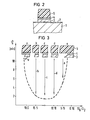
- FIG. 1 is the silicon substrate, 2 the SiO 2 layer thereon, 3 the n + -doped polysilicon layer, 4 the silicide layer, 5 the photoresist layer serving as an etching mask, 6 the poly-silicon-1- Gate structure and with 7 the insulation oxide located thereon.
- the same reference numerals apply to the same parts.
- the vertical arrows drawn in FIG. 1 each indicate the etching problem that is to be solved by the method according to the teaching of the invention.
- the layer thickness ratio of polycide double layer (3, 4): Si0 2 (2) is up to 20: 1.
- the arrow 11 shows the achievement of a suitable edge shape in the etched structures. This can be done either by anisotropic etching with vertical edges, as shown, or by chamfered etching.
- the arrow 12 is intended to indicate the step problem in a double poly silicon gate process with the risk of electrical short circuits due to etching residues on polysilicon 1 edges (6, 7).
- the arrow 13 indicates the formation of the contact polycide (3, 4) to the substrate (1), the so-called buried contact.
- the invention also has the task of using a photoresist mask as the etching mask should be usable, which is not attacked by the etching process.
- a photoresist mask as the etching mask should be usable, which is not attacked by the etching process.
- etching is carried out partly in the tunnel reactor, partly in the parallel plate reactor in anodic coupling ("plasma etching") (see also J. Vac. Sci. Technol. 18 (2) March 1981, p. 346).
- plasma etching anodic coupling
- these layers can also be etched wet, but only with the loss of size usual for wet etching.
- the method according to the teaching of the invention goes beyond this prior art for the etching of a metal silicide / polysilicon double layer (called a polycide layer) and also solves the problem of the beveled etching or the step problem in a double poly silicon gate process without the risk of electrical short-circuits of adjacent polycide tracks (see Figure 1, arrows 1.1, 12 and 13).
- the method according to the teaching of the invention is characterized in that a gas mixture which contains fluorine and chlorine is used as the reactive gas. If only an etching gas containing fluorine, such as sulfur hexafluoride, were used, an overhang would be formed. On the other hand, the use of only chlorine as the etching gas, especially in the case of tantalum silicide layers, brings very low etching rates. It is therefore within the scope of the invention to use a gas mixture consisting of sulfur hexafluoride (SF 6 ) and chlorine (Cl 2 ).
- SF 6 sulfur hexafluoride
- Cl 2 chlorine
- fluorocarbons substituted by chlorine atoms such as monochlorotrifluoromethane (CC1F 3 ) or dichlorodifluoromethane (CCl 2 F 2 ).
- a double layer which consists of an approximately 200 nm thick tantalum silicide layer, the tantalum: silicon ratio being 1: 2, and a 300 nm thick n + -doped polysili layer.
- the structure shown in FIG. 2 consists of a 300 nm thick n-doped (phosphorus or arsenic) polysilicon layer 3 and a 200 nm thick tantalum silicide layer 4 deposited on a silicon substrate 1 provided with a 20 nm thick SiO 2 layer 2.
- the photoresist layer used as an etching mask is designated by 5.
- the tantalum: silicon ratio is approximately 1: 2 (fluctuations in the Ta: Si ratio are permitted at 30% - 50% Ta).
- a structure is shown in FIG. 2 in which a strict anisotropic etching was desired. This can e.g.
- the switchover point from the first to the second stage can e.g. B. by recording the intensity of a suitable emission line of the plasma ..
- a very high selectivity poly-Si to SiO 2 of> 30: 1 can be achieved.
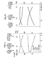
- FIG. 3 shows how the edge profiles of the double layer 3, 4 change with the composition of the etching gas mixture.
- the mixing ratio SF 6 : C1 2 is the abscissa and the etching time is the ordinate applied for the double layer.
- the dashed curve drawn in the figure shows the dependence of the etching time on the gas composition.
- Structure a shows a structure etched without chlorine components with a long etching time (see arrow a).
- Structure b has a very low etching time (see arrow b).
- FIGS. 4 and 5 show the etching speed in nm / min as a function of the gas pressure in Pa (FIG. 4) and the HF power in watts / cm 2 (FIG. 5).
- the arrows mark the conditions under which the structures shown were obtained.
- the arrows for the structures with the most favorable conditions are marked more strongly.
- an RF power of 0.1 W / cm was set.
- the x-dashed curve applies to tantalum silicide, the o-dashed curve for polysilicon, the 0-dashed curve for SiO 2 and the curve with S-dashed curve shows the selectivities of polysilicon: Si0 2 .
- FIGS. 6 and 7 It was found that, with a constant gas mixture, the etching profile also depends sensitively on the reactor geometry, that is to say on the ratio of active or plasma volume to the total volume of the reactor. The ratio influences the concentration distribution of the various radicals in the plasma. In the structure depicted in FIG. 6, the ratio of the active volume to the reactor volume was ⁇ 1:20, while in FIG. 7 the ratio was approximately 1: 2, that is to say the active volume corresponded to half the reactor volume. The main difference is that in the first case the silicide (the upper layer) etches anisotropically with respect to the photoresist mask in all SF 6 : Cl 2 ratios. In the second case, the silicide etching behavior can be varied from anisotropic to severe under-etching via the mixing ratio (see FIG. 3).
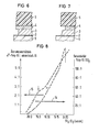
- Figure 8 If the polycide layer (3, 4) is to have local contact with the silicon substrate (buried contact), a certain etching of the substrate (1) cannot be avoided (see Figure 1, arrow 13). This can lead to increased contact resistances between the polycide and the substrate at the end of the circuit manufacturing process. With proper choice of the fluoro-chloro-ratio in the reaction gas can be relatively high (up to 10: 1) selectivity of n + - polysilicon: silicon - reach substrate and thus keep the etching of the substrate is very low. These relationships can be seen in FIG. 8.
- the curve marked with arrow 14 applies to the selectivity, that with arrow 15 applies to the etching speed ratio.
- the markings shown represent measuring points.
- the most favorable range for a gas mixture ratio SF 6 : Cl 2 is between 5:15 and 2:18.
- the silicide is made polycrystalline and of low resistance.
- the silicide / polysilicon layer interface is much more homogeneous, that is to say less rough than after the tempering. This has the advantage that the switchover point can be better defined when etching in a two-stage process.
Abstract
Die Erfindung betrifft ein Verfahren zum Herstellen von Strukturen von aus Metallsilizid (4) und Polysilizium (3) bestehenden Doppelschichten auf integrierte Halbleiterschaltungen enthaltenden Siliziumsubstraten (1) durch reaktives Ionenätzen unter Verwendung einer Fotolackmaske (5), bei dem in einem Plattenreaktor als reaktives Gas ein Gasgemisch verwendet wird, das Fluor und Chlor enthält. Die Doppelschicht (3, 4) besteht vorzugsweise aus einer Tantalsilizid/Polysiliziumschicht. Das Verfahren wird insbesondere verwendet für die Herstellung niederohmiger Leiterbahnen in VLSI-Schaltungen.The invention relates to a method for producing structures of double layers consisting of metal silicide (4) and polysilicon (3) on silicon substrates (1) containing integrated semiconductor circuits by reactive ion etching using a photoresist mask (5), in which a reactive gas is used in a plate reactor Gas mixture is used that contains fluorine and chlorine. The double layer (3, 4) preferably consists of a tantalum silicide / polysilicon layer. The method is used in particular for the production of low-resistance conductor tracks in VLSI circuits.
Description
Die Erfindung betrifft ein Verfahren zum Herstellen von Strukturen von aus Metallsilizid/Polysilizium bestehenden Doppelschichten (auch Polyzid genannt) auf integrierte Halbleiterschaltungen enthaltenden, vorzugsweise mit einer Isolationsschicht versehenen Siliziumsubstraten durch reaktives Ionenätzen in einem Plattenreaktor mit einem Halogene enthaltenden Gasgemisch unter Verwendung einer Fotolackmaske.The invention relates to a method for producing structures of double layers consisting of metal silicide / polysilicon (also called polycide) on silicon substrates containing integrated semiconductor circuits, preferably provided with an insulation layer, by reactive ion etching in a plate reactor with a gas mixture containing halogens using a photoresist mask.
Metallsilizide finden bei der Herstellung von hochintegrierten MOS-Schaltungen zunehmende Bedeutung. Eine der möglichen Anwendungen ist ihre Verwendung als niederohmiges Leitbahn- und Gatematerial in einem Poly- silizium-Gate-Prozeß. Das bewährte Polysilizium wird dabei im allgemeinen nicht durch das Silizid ersetzt, sondern ergänzt, und zwar in der Form, daß man über einer dotierten Polysiliziumschicht das Silizid aufbringt. Die Erzeugung feiner Strukturen in solchen Doppelschichten ist ein komplexes Ätzproblem, da bei der Herstellung von integrierten Schaltungen eine Reihe von Randbedingungen zu beachten sind.Metal silicides are becoming increasingly important in the manufacture of highly integrated MOS circuits. One of the possible applications is their use as a low-resistance interconnect and gate material in a polysilicon gate process. The tried-and-tested polysilicon is generally not replaced by the silicide, but is supplemented, in such a way that the silicide is applied over a doped polysilicon layer. The generation of fine structures in such double layers is a complex etching problem, since a number of boundary conditions have to be taken into account when manufacturing integrated circuits.
Die Lösung dieses komplexen Ätzproblems ist Aufgabe der vorliegenden Erfindung.The object of the present invention is to solve this complex etching problem.
Anhand der in der Zeichnung abgebildeten Figur 1 sollen die Randbedingungen, die beim Ätzprozeß bei der Herstellung einer integrierten Schaltung beachtet werden müssen, näher erläutert werden. Dabei ist mit dem Bezugszeichen 1 das Siliziumsubstrat, mit 2 die darauf befindliche Si02-Schicht, mit 3 die n+-dotierte Polysiliziumschicht, mit 4 die Silizidschicht, mit 5 die als Ätzmaske dienende Fotolackschicht, mit 6 die Poly-Silizium-1-Gatestruktur und mit 7 das darauf befindliche Isolationsoxid bezeichnet. In allen Figuren der vorliegenden Patentanmeldungen gelten für gleiche Teile gleiche Bezugszeichen. Die in Figur 1 eingezeichneten senkrechten Pfeile zeigen jeweils das Ätzproblem an, das durch das Verfahren nach der Lehre der Erfindung gelöst werden soll.Using the figure 1 shown in the drawing, the boundary conditions that arise during the etching process in the Position of an integrated circuit must be considered, are explained in more detail. 1 is the silicon substrate, 2 the SiO 2 layer thereon, 3 the n + -doped polysilicon layer, 4 the silicide layer, 5 the photoresist layer serving as an etching mask, 6 the poly-silicon-1- Gate structure and with 7 the insulation oxide located thereon. In all figures of the present patent applications, the same reference numerals apply to the same parts. The vertical arrows drawn in FIG. 1 each indicate the etching problem that is to be solved by the method according to the teaching of the invention.
So zeigt der Pfeil 10 die angestrebte hohe Selektivität zu Si02 (2) oder einem anderen entsprechenden Isolatormaterial. Das Schichtdickenverhältnis Polyzid-Doppelschicht (3, 4) : Si02 (2) beträgt bis zu 20:1.So the
Der Pfeil 11 zeigt die Erzielung einer geeigneten Kantenform in den geätzten Strukturen. Dies kann entweder durch anisotropes Ätzen mit senkrechten Kanten, wie dargestellt, oder durch abgeschrägtes Ätzen erfolgen.The
Der Pfeil 12 soll das Stufenproblem in einem Doppel-Poly-Silizium-Gateprozeß mit der Gefahr von elektrischen Kurzschlüssen durch Ätzrückstände an Polysilizium 1-Kanten (6, 7) andeuten.The
Der Pfeil 13 weist auf die Ausbildung des Kontaktes Polyzid (3, 4) zum Substrat (1), dem sogenannten buried contact hin.The
Neben diesen Bedingungen, die durch das erfindungsgemäße Verfahren zu erfüllen sind, hat die Erfindung noch die Aufgabe, daß als Ätzmaske eine Fotolackmaske verwendbar sein soll, welche durch den Ätzprozeß nicht angegriffen wird. Außerdem soll in allen Bereichen, wegen des sogenannten Kurzkanaleffektes, eine hohe Ätzgleichmäßigkeit vorhanden sein.In addition to these conditions, which are to be met by the method according to the invention, the invention also has the task of using a photoresist mask as the etching mask should be usable, which is not attacked by the etching process. In addition, due to the so-called short-channel effect, there should be a high etching uniformity in all areas.
Aus dem Stand der Technik ist bekannt, Strukturen von Polysiliziden zu ätzen, wobei in fast allen bekannten Fällen Molybdän- und Wolframsilizide geätzt werden. Über die Ätzung von Tantalsilizidstrukturen, welches gegenüber Molybdän- und Wolframsiliziden wegen der besseren Temperaturstabilität bei hohen Temperaturen und der guten Hafteigenschaften auf Polysilizium erhebliche Vorteile hat, gibt es nur einen kurzen Hinweis in J. Vac. Sci. Technol. 17 (4) July/Aug.1980 p.787/788, aus dem zu entnehmen ist, daß Titan-, Tantal-, Molybdän- und Wolfram-Silizide im Plasma in einer TetrafluorKohlenstoff-Sauerstoff-Mischung zu ätzen sind. Dabei werden die Ätzungen teils im Tunnelreaktor, teils im Parallelplattenreaktor in anodischer Kopplung ("Plasmaätzen") durchgeführt (siehe auch J. Vac. Sci. Technol. 18 (2) March 1981, p. 346). Im Prinzip können diese Schichten auch'naß geätzt werden, jedoch nur mit dem für Naßätzung üblichen Maßverlust.It is known from the prior art to etch structures of polysilicicides, with molybdenum and tungsten silicides being etched in almost all known cases. There is only a brief note in J. Vac about the etching of tantalum silicide structures, which has considerable advantages over molybdenum and tungsten silicides because of the better temperature stability at high temperatures and the good adhesive properties on polysilicon. Sci. Technol. 17 (4) July / Aug.1980 p.787 / 788, from which it can be seen that titanium, tantalum, molybdenum and tungsten silicides are to be etched in plasma in a tetrafluorocarbon-oxygen mixture. The etching is carried out partly in the tunnel reactor, partly in the parallel plate reactor in anodic coupling ("plasma etching") (see also J. Vac. Sci. Technol. 18 (2) March 1981, p. 346). In principle, these layers can also be etched wet, but only with the loss of size usual for wet etching.
Aus der europäischen Patentanmeldung 0 015 403 sind mehrere Verfahren zum Plasmaätzen von Polysilizium zu entnehmen, wobei von Gasmischungen bestehend aus Schwefelhexafluorid (SF6), Chlor (C12) und einem Inertgas ausgegangen wird. Bei diesen Verfahren wird aber nur Silizium selektiv geätzt, wobei eine sehr gute Selektivität in Gegenwart von SiO2 und Siliziumnitrid erzielt wird. Daneben wird auch, bedingt durch das reaktive Ionenätzen (die zu ätzenden Substrate werden auf die HF-führende Elektrode gelegt) eine gerichtete Ätzung durchgeführt, so daß die erzeugten Vertiefungen senkrechte Seitenwände haben und die Ätzmaske über den Rand der geätzten Vertiefungen nicht hinausragt.Several methods for plasma etching of polysilicon can be found in
Ein Verfahren der eingangs genannten Art ist in der Patentanmeldung P 30 45 922.4 vorgeschlagen worden. Bei diesem Verfahren wird Schwefelhexafluorid als Ätzgas verwendet und der Ätzprozeß in zwei Schritten mit unterschiedlichen Ätzraten durchgeführt. Auch bei diesem Ätzprozeß wird eine strenge Anisotropie angestrebt.A method of the type mentioned has been proposed in patent application P 30 45 922.4. In this method, sulfur hexafluoride is used as the etching gas and the etching process is carried out in two steps with different etching rates. A strict anisotropy is also sought in this etching process.
Das Verfahren nach der Lehre der Erfindung geht über diesen Stand der Technik für die Ätzung einer Metallsilizid/Polysilizium-Doppelschicht (genannt PolyzidSchicht) hinaus und löst auch noch das Problem der abgeschrägten Ätzung bzw. das Stufenproblem in einem Doppel-Poly-Silizium-Gateprozeß ohne die Gefahr von elektrischen Kurzschlüssen benachbarter Polyzidbahnen (siehe Figur 1, Pfeile 1.1, 12 und 13).The method according to the teaching of the invention goes beyond this prior art for the etching of a metal silicide / polysilicon double layer (called a polycide layer) and also solves the problem of the beveled etching or the step problem in a double poly silicon gate process without the risk of electrical short-circuits of adjacent polycide tracks (see Figure 1, arrows 1.1, 12 and 13).
Das Verfahren nach der Lehre der Erfindung ist dadurch gekennzeichnet, daß als reaktives Gas ein Gasgemisch verwendet wird, welches Fluor und Chlor enthält. Würde man nur ein Fluor enthaltendes Ätzgas wie Schwefelhexafluorid verwenden, so würde sich ein Überhang ausbilden. Andererseits bringt die Verwendung von nur Chlor als Ätzgas, insbesondere bei Tantalsilizidschichten sehr.niedrige Ätzraten. Es liegt daher im Rahmen der Erfindung, eine aus Schwefelhexafluorid (SF6) und Chlor (Cl2) bestehende Gasmischung zu verwenden.The method according to the teaching of the invention is characterized in that a gas mixture which contains fluorine and chlorine is used as the reactive gas. If only an etching gas containing fluorine, such as sulfur hexafluoride, were used, an overhang would be formed. On the other hand, the use of only chlorine as the etching gas, especially in the case of tantalum silicide layers, brings very low etching rates. It is therefore within the scope of the invention to use a gas mixture consisting of sulfur hexafluoride (SF 6 ) and chlorine (Cl 2 ).
Es ist aber auch möglich, durch Chloratome substituierte Fluorkohlenwasserstoffe, wie Monochlortrifluormethan (CC1F3) oder Dichlordifluormethan (CCl2F2) einzusetzen.However, it is also possible to use fluorocarbons substituted by chlorine atoms, such as monochlorotrifluoromethane (CC1F 3 ) or dichlorodifluoromethane (CCl 2 F 2 ).
Gemäß einem besonders günstigen Ausführungsbeispiel nach der Lehre der Erfindung wird eine Doppelschicht verwendet, welche aus einer etwa 200 nm dicken Tantalsilizidschicht, wobei das Tantal:Silizium-Verhältnis wie 1:2 ist, und aus einer 300 nm dicken n+-dotierten Polysiliziumschicht besteht.According to a particularly favorable embodiment according to the teaching of the invention, a double layer is used, which consists of an approximately 200 nm thick tantalum silicide layer, the tantalum: silicon ratio being 1: 2, and a 300 nm thick n + -doped polysili layer.
Andere Ausgestaltungen der Erfindung ergeben sich aus den Unteransprüchen.Other configurations of the invention result from the subclaims.
Weitere Einzelheiten sowie Vorteile des erfindungsgemäßen Verfahrens werden im folgenden anhand von Ausführungsbeispielen und der Figuren 2 bis 8 noch näher erläutert. Dabei zeigt
- die
Figur 2 im Schnittbild eine gemäß der Lehre der Erfindung hergestellte Struktur, - die
Figuren - die
Figuren 6 und 7 die mit unterschiedlichem Volumenverhältnis (aktives Volumen : Reaktorvolumen) erhaltenen Strukturen und - die
Figur 8 das Ätzratenverhältnis n+-dotiertes Poly- silizium zu einkristallinem Silizium bzw. die Selektivität Polysilizium zu SiO2 in Abhängigkeit von der Gasmischung.
- 2 is a sectional view of a structure produced according to the teaching of the invention,
- FIGS. 3, 4 and 5 in a diagram the optimal etching conditions (mixing ratio of the gases, etching time, gas pressure and RF power) with the structures achieved thereby,
- FIGS. 6 and 7 show the structures obtained with different volume ratios (active volume: reactor volume) and
- 8 shows the etching rate ratio n + - doped polysilicon to single-crystalline silicon or the selectivity polysilicon to SiO 2 as a function of the gas mixture.
Die in Figur 2 dargestellte Struktur besteht aus einer 300 nm dicken, auf einem mit einem 20 nm dicken Si02- .Schicht 2 versehenen Siliziumsubstrat 1 aufgebrachten n -dotierten (Phosphor oder Arsen) Polysiliziumschicht 3 und einer darüber abgeschiedenen 200 nm dicken Tantalsilizidschicht 4. Mit 5 ist die als Ätzmaske verwendete Photolackschicht bezeichnet. Das Tantal:Silizium-Verhältnis beträgt ungefähr 1:2 (Schwankungen des Ta:Si-Verhältnisses sind zugelassen bei 30 % - 50 % Ta). In Figur 2 ist eine Struktur abgebildet, bei der ein strikt anisotropes Ätzen angestrebt wurde. Dies kann z. B: durch einen Zweistufenprozeß erreicht werden, indem zunächst das Tantalsilizid (4) mit geringem Chloranteil im Ätzgas geätzt'und anschließend das Polysilizium (3) in reinem Chlor behandelt wird. Auf diese Weise können Silizid-Polysilizium-Doppelschichten völlig unter- ätzungsfrei mit senkrechten Kanten, wie in Figur 2 dargestellt, erhalten werden. Der Umschaltpunkt von der ersten zur zweiten Stufe kann z. B. durch Aufzeichnung der Intensität einer geeigneten Emissionslinie des Plasmas festgelegt werden..Gleichzeitig kann man in der zweiten Stufe (mit reinem C12) eine sehr hohe Selektivität Poly-Si zu SiO2 von > 30:1 erreichen.The structure shown in FIG. 2 consists of a 300 nm thick n-doped (phosphorus or arsenic)
Aus Figur 3 ist ersichtlich, wie sich die Kantenprofile der Doppelschicht 3, 4 mit der Zusammensetzung der Ätzgasmischung ändern. Dabei ist als Abszisse das Mischungsverhältnis SF6:C12 und als Ordinate die Ätzzeit ![]()
![]()
Der Gasdruck im Reaktor betrug bei den Ätzungen in Figur 3 6 bis 9 Pa (= 40 bis 60 mTorr), die HF-Leistung ~ 0.12 W/cm2.The gas pressure in the reactor during the etching in FIG. 3 was 6 to 9 Pa (= 40 to 60 mTorr), the HF power was ~ 0.12 W / cm2.
In den Figuren 4 und 5 ist die Ätzgeschwindigkeit in nm/min in Abhängigkeit vom Gasdruck in Pa (Figur 4) und der HF-Leistung in Watt/cm2 (Figur 5) aufgetragen. Die Pfeile markieren die Bedingungen, unter denen die eingezeichneten Strukturen erhalten wurden. Die Pfeile für die Strukturen mit den günstigsten Bedingungen sind stärker ausgezeichnet. Bei dem in Figur 4 dargestellten Diagramm wurde eine HF-Leistung von 0,1 W/cm eingestellt. Die Gasmischung hatte ein Mischungsverhältnis SF6:Cl2:He (Helium) = 12,5:6,5:20. Die x-gestrichelte Kurve gilt für Tantalsilizid, die o-gestrichelte Kurve für Polysilizium, die 0 -gestrichelte Kurve für SiO2 und die mit S-gestrichelte Kurve zeigt die Selektivitäten von Polysilizium : Si02.FIGS. 4 and 5 show the etching speed in nm / min as a function of the gas pressure in Pa (FIG. 4) and the HF power in watts / cm 2 (FIG. 5). The arrows mark the conditions under which the structures shown were obtained. The arrows for the structures with the most favorable conditions are marked more strongly. In the diagram shown in FIG. 4, an RF power of 0.1 W / cm was set. The gas mixture had a mixing ratio SF 6 : Cl 2 : He (helium) = 12.5: 6.5: 20. The x-dashed curve applies to tantalum silicide, the o-dashed curve for polysilicon, the 0-dashed curve for SiO 2 and the curve with S-dashed curve shows the selectivities of polysilicon: Si0 2 .
Das gleiche gilt auch für das in Figur 5 eingezeichnete Kurvendiagramm, welches die Abhängigkeit von der HF-Leistung (Watt cm2) darstellt. Der Gasdruck im Reaktor betrug 40 m Torr.The same also applies to the curve diagram drawn in FIG. 5, which shows the dependence on the HF power (watt cm 2 ). The gas pressure in the reactor was 40 m torr.
Figur 6 und 7: Es wurde festgestellt, daß bei konstanter Gasmischung das Ätzprofil empfindlich auch von der Reaktorgeometrie abhängt, das heißt vom Verhältnis aktives oder Plasmavolumen zu Gesamtvolumen des Reaktors. Das Verhältnis beeinflußt die Konzentrationsverteilung der verschiedenen Radikale im Plasma. Bei der in Figur 6 abgbildeten Struktur lag ein Verhältnis des aktiven Volumens zum Reaktorvolumen von <1:20 vor, während bei Figur 7 das Verhältnis etwa 1:2 betrug, das heißt, das aktive Volumen entsprach der Hälfte des Reaktorvolumens. Der wesentliche Unterschied besteht darin, daß im ersten Fall das Silizid (die obere Schicht) bei allen SF6:Cl2-Verhältnissen anisotrop bezüglich der Fotolackmaske ätzt. Im zweiten Fall kann man über das Mischungsverhältnis das Silizidätzverhalten von anisotrop bis zu starkem Unterätzen variieren (s. Figur 3).FIGS. 6 and 7: It was found that, with a constant gas mixture, the etching profile also depends sensitively on the reactor geometry, that is to say on the ratio of active or plasma volume to the total volume of the reactor. The ratio influences the concentration distribution of the various radicals in the plasma. In the structure depicted in FIG. 6, the ratio of the active volume to the reactor volume was <1:20, while in FIG. 7 the ratio was approximately 1: 2, that is to say the active volume corresponded to half the reactor volume. The main difference is that in the first case the silicide (the upper layer) etches anisotropically with respect to the photoresist mask in all SF 6 : Cl 2 ratios. In the second case, the silicide etching behavior can be varied from anisotropic to severe under-etching via the mixing ratio (see FIG. 3).
Figur 8: Wenn die Polyzidschicht (3, 4) lokal einen Kontakt zum Siliziumsubstrat (buried contact) haben soll, ist naturgemäß ein gewisses Anätzen des Substrats (1) nicht zu vermeiden (siehe Figur 1, Pfeil 13). Dies kann am Ende des Herstellungsprozesses einer Schaltung zu erhöhten Übergangswiderständen zwischen Polyzid und Substrat führen. Bei richtiger Wahl des Fluor-Chlor-Verhältnisses im Reaktionsgas kann man eine relativ hohe (bis zu 10:1) Selektivität von n+-Polysilizium:Silizium- substrat erreichen und damit das Anätzen des Substrats sehr gering halten. Diese Verhältnisse sind aus Figur 8 zu entnehmen. Das Diagramm zeigt das Ätzratenverhältnis n+-Polysilizium : einkristallines Silizium bzw. die Selektivität n+-Polysilizium : Si02 in Abhängigkeit vom Gasmischungsverhältnis SF6:Cl2 in sccm (= standard-cm3 pro min, dabei bedeutet Standard bei atmosphärischem Druck und definierter Temperatur). Die mit dem Pfeil 14 gekennzeichnete Kurve gilt für die Selektivität, die mit dem Pfeil 15 für das Ätzgeschwindigkeitsverhältnis. Die eingezeichneten Markierungen stellen Meßpunkte dar. Der günstigste Bereich liegt bei einem Gasmischungsverhältnis SF6:Cl2 zwischen 5:15 und 2:18.Figure 8: If the polycide layer (3, 4) is to have local contact with the silicon substrate (buried contact), a certain etching of the substrate (1) cannot be avoided (see Figure 1, arrow 13). This can lead to increased contact resistances between the polycide and the substrate at the end of the circuit manufacturing process. With proper choice of the fluoro-chloro-ratio in the reaction gas can be relatively high (up to 10: 1) selectivity of n + - polysilicon: silicon - reach substrate and thus keep the etching of the substrate is very low. These relationships can be seen in FIG. 8. The diagram shows the etching rate ratio of n + polysilicon: single-crystalline silicon and the selectivity of n + polysilicon: Si0 2 as a function of the gas mixture ratio SF 6 : Cl 2 in sccm (= standard cm 3 per min, where standard means at atmospheric pressure and defined temperature). The curve marked with
Es liegt im Rahmen des Erfindungsgedankens, das Strukturieren des Polyzids (3, 4) vor dem Tempern, durch welches das Silizid polykristallin und niederohmig gemacht wird, durchzuführen. Vor dem Tempern ist die Grenzfläche Silizid/Polysiliziumschicht sehr viel homogener, das heißt weniger rauh als nach dem Tempern. Dies hat den Vorteil, daß der Umschaltpunkt beim Ätzen in einem Zweistufenprozeß besser zu definieren ist.It is within the scope of the inventive concept to carry out the structuring of the polycide (3, 4) before the annealing, by means of which the silicide is made polycrystalline and of low resistance. Before the tempering, the silicide / polysilicon layer interface is much more homogeneous, that is to say less rough than after the tempering. This has the advantage that the switchover point can be better defined when etching in a two-stage process.
Claims (11)
Applications Claiming Priority (2)
| Application Number | Priority Date | Filing Date | Title |
|---|---|---|---|
| DE3216823 | 1982-05-05 | ||
| DE19823216823 DE3216823A1 (en) | 1982-05-05 | 1982-05-05 | METHOD FOR PRODUCING STRUCTURES OF DOUBLE LAYERS CONSISTING OF METAL SILICIDE AND POLYSILIZIUM ON SUBSTRATES CONTAINING INTEGRATED SEMICONDUCTOR CIRCUITS BY REACTIVE ION NETWORK |
Publications (2)
| Publication Number | Publication Date |
|---|---|
| EP0094528A2 true EP0094528A2 (en) | 1983-11-23 |
| EP0094528A3 EP0094528A3 (en) | 1987-05-06 |
Family
ID=6162783
Family Applications (1)
| Application Number | Title | Priority Date | Filing Date |
|---|---|---|---|
| EP83104121A Withdrawn EP0094528A3 (en) | 1982-05-05 | 1983-04-27 | Process for producing double-layer structures consisting of metal silicide and polysilicium on substrates containing integrated circuits by reactive ion etching |
Country Status (4)
| Country | Link |
|---|---|
| US (1) | US4473436A (en) |
| EP (1) | EP0094528A3 (en) |
| JP (1) | JPS58204538A (en) |
| DE (1) | DE3216823A1 (en) |
Cited By (3)
| Publication number | Priority date | Publication date | Assignee | Title |
|---|---|---|---|---|
| EP0126969A2 (en) * | 1983-04-29 | 1984-12-05 | Siemens Aktiengesellschaft | Process for manufacturing structures comprising metallic silicides, especially silicide-polysilicon, for integrated semiconductor circuits using reactive ion etching |
| EP0256311A2 (en) * | 1986-08-09 | 1988-02-24 | International Business Machines Corporation | RIE process for etching silicon isolation trenches and polycides with vertical surfaces |
| EP0516043A2 (en) * | 1991-05-29 | 1992-12-02 | Tokyo Electron Limited | Dry etching method |
Families Citing this family (27)
| Publication number | Priority date | Publication date | Assignee | Title |
|---|---|---|---|---|
| US4659426A (en) * | 1985-05-03 | 1987-04-21 | Texas Instruments Incorporated | Plasma etching of refractory metals and their silicides |
| US4624739A (en) * | 1985-08-09 | 1986-11-25 | International Business Machines Corporation | Process using dry etchant to avoid mask-and-etch cycle |
| US4734157A (en) * | 1985-08-27 | 1988-03-29 | International Business Machines Corporation | Selective and anisotropic dry etching |
| JPH0628290B2 (en) * | 1985-10-09 | 1994-04-13 | 三菱電機株式会社 | Semiconductor device with circuit fuse |
| US4713141A (en) * | 1986-09-22 | 1987-12-15 | Intel Corporation | Anisotropic plasma etching of tungsten |
| EP0565212A2 (en) * | 1986-12-19 | 1993-10-13 | Applied Materials, Inc. | Iodine etch process for silicon and silicides |
| US4836886A (en) * | 1987-11-23 | 1989-06-06 | International Business Machines Corporation | Binary chlorofluorocarbon chemistry for plasma etching |
| JP2506151B2 (en) * | 1988-06-15 | 1996-06-12 | シャープ株式会社 | Method for manufacturing semiconductor device |
| US4981816A (en) * | 1988-10-27 | 1991-01-01 | General Electric Company | MO/TI Contact to silicon |
| US5201993A (en) * | 1989-07-20 | 1993-04-13 | Micron Technology, Inc. | Anisotropic etch method |
| US5271799A (en) * | 1989-07-20 | 1993-12-21 | Micron Technology, Inc. | Anisotropic etch method |
| US5110411A (en) * | 1990-04-27 | 1992-05-05 | Micron Technology, Inc. | Method of isotropically dry etching a poly/WSix sandwich structure |
| US5160408A (en) * | 1990-04-27 | 1992-11-03 | Micron Technology, Inc. | Method of isotropically dry etching a polysilicon containing runner with pulsed power |
| KR0176715B1 (en) * | 1990-07-30 | 1999-04-15 | 오가 노리오 | Dry etching method |
| US5094712A (en) * | 1990-10-09 | 1992-03-10 | Micron Technology, Inc. | One chamber in-situ etch process for oxide and conductive material |
| US5160407A (en) * | 1991-01-02 | 1992-11-03 | Applied Materials, Inc. | Low pressure anisotropic etch process for tantalum silicide or titanium silicide layer formed over polysilicon layer deposited on silicon oxide layer on semiconductor wafer |
| US5658425A (en) * | 1991-10-16 | 1997-08-19 | Lam Research Corporation | Method of etching contact openings with reduced removal rate of underlying electrically conductive titanium silicide layer |
| US5269879A (en) * | 1991-10-16 | 1993-12-14 | Lam Research Corporation | Method of etching vias without sputtering of underlying electrically conductive layer |
| US5354417A (en) * | 1993-10-13 | 1994-10-11 | Applied Materials, Inc. | Etching MoSi2 using SF6, HBr and O2 |
| JPH10270430A (en) | 1997-03-27 | 1998-10-09 | Mitsubishi Electric Corp | Plasma treating device |
| JPH10270428A (en) * | 1997-03-27 | 1998-10-09 | Mitsubishi Electric Corp | Plasma treating device |
| US5856239A (en) * | 1997-05-02 | 1999-01-05 | National Semiconductor Corporaton | Tungsten silicide/ tungsten polycide anisotropic dry etch process |
| JP3336975B2 (en) * | 1998-03-27 | 2002-10-21 | 日本電気株式会社 | Substrate processing method |
| US6074954A (en) * | 1998-08-31 | 2000-06-13 | Applied Materials, Inc | Process for control of the shape of the etch front in the etching of polysilicon |
| KR100430950B1 (en) * | 1998-09-01 | 2004-06-16 | 엘지.필립스 엘시디 주식회사 | Thin film transistor and its manufacturing method |
| DE10244862B4 (en) * | 2002-09-23 | 2006-09-14 | IHP GmbH - Innovations for High Performance Microelectronics/Institut für innovative Mikroelektronik | Method for producing an electronic component with a praseodymium oxide layer |
| US20140199833A1 (en) * | 2013-01-11 | 2014-07-17 | Applied Materials, Inc. | Methods for performing a via reveal etching process for forming through-silicon vias in a substrate |
Citations (2)
| Publication number | Priority date | Publication date | Assignee | Title |
|---|---|---|---|---|
| JPS5731140A (en) * | 1980-07-31 | 1982-02-19 | Toshiba Corp | Etching method by reactive ion |
| GB2098931A (en) * | 1981-05-22 | 1982-12-01 | Western Electric Co | Method of plasma etching microminiature devices |
Family Cites Families (12)
| Publication number | Priority date | Publication date | Assignee | Title |
|---|---|---|---|---|
| JPS537549A (en) * | 1976-07-09 | 1978-01-24 | Mitsubishi Electric Corp | Etchant for dry etching |
| US4128670A (en) * | 1977-11-11 | 1978-12-05 | International Business Machines Corporation | Fabrication method for integrated circuits with polysilicon lines having low sheet resistance |
| US4203800A (en) * | 1977-12-30 | 1980-05-20 | International Business Machines Corporation | Reactive ion etching process for metals |
| US4211601A (en) * | 1978-07-31 | 1980-07-08 | Bell Telephone Laboratories, Incorporated | Device fabrication by plasma etching |
| US4214946A (en) * | 1979-02-21 | 1980-07-29 | International Business Machines Corporation | Selective reactive ion etching of polysilicon against SiO2 utilizing SF6 -Cl2 -inert gas etchant |
| JPS5626450A (en) * | 1979-08-13 | 1981-03-14 | Hitachi Ltd | Manufacture of semiconductor device |
| US4383885A (en) * | 1980-02-06 | 1983-05-17 | Bell Telephone Laboratories, Incorporated | Reactive sputter etching of polysilicon utilizing a chlorine etch gas |
| DE3045922A1 (en) * | 1980-12-05 | 1982-07-08 | Siemens AG, 1000 Berlin und 8000 München | METHOD FOR PRODUCING STRUCTURES OF LAYERS CONSTRUCTED FROM SILICIDES OR FROM SILICIDE-POLYSILIZIUM BY REACTIVE SPUTTERING |
| DE3103177A1 (en) * | 1981-01-30 | 1982-08-26 | Siemens AG, 1000 Berlin und 8000 München | METHOD FOR PRODUCING POLYSILIZIUM STRUCTURES UP TO THE 1 (MY) M AREA ON SUBSTRATES CONTAINING INTEGRATED SEMICONDUCTOR CIRCUITS BY PLASMA |
| US4384938A (en) * | 1982-05-03 | 1983-05-24 | International Business Machines Corporation | Reactive ion etching chamber |
| US4414057A (en) * | 1982-12-03 | 1983-11-08 | Inmos Corporation | Anisotropic silicide etching process |
| US4411734A (en) * | 1982-12-09 | 1983-10-25 | Rca Corporation | Etching of tantalum silicide/doped polysilicon structures |
-
1982
- 1982-05-05 DE DE19823216823 patent/DE3216823A1/en not_active Withdrawn
-
1983
- 1983-04-27 EP EP83104121A patent/EP0094528A3/en not_active Withdrawn
- 1983-05-02 JP JP58078103A patent/JPS58204538A/en active Pending
- 1983-05-02 US US06/490,481 patent/US4473436A/en not_active Expired - Lifetime
Patent Citations (2)
| Publication number | Priority date | Publication date | Assignee | Title |
|---|---|---|---|---|
| JPS5731140A (en) * | 1980-07-31 | 1982-02-19 | Toshiba Corp | Etching method by reactive ion |
| GB2098931A (en) * | 1981-05-22 | 1982-12-01 | Western Electric Co | Method of plasma etching microminiature devices |
Non-Patent Citations (6)
| Title |
|---|
| EXTENDED ABSTRACTS, Band 81-1, Mai 1981, Seiten 586-588, Pennington, New Jersey, US; W. BEINVOGL et al.: "Anisotropic etching of polysilicon and metal silicides in fluorine containing plasma" * |
| EXTENDED ABSTRACTS, Band 81-2, Oktober 1981, Seiten 652-654, Pennington, New Jersey, US; W.W. YAO et al.: "Anisotropic polysilicon etching with Cl2 plasma" * |
| JOURNAL OF THE ELECTROCHEMICAL SOCIETY, Band 128, Nr. 2, Februar 1981, Seiten 366-370, Manchester, New Hampshire, US; A.C. ADAMS et al.: "Edge profiles in the plasma etching of polycrystalline silicon" * |
| JOURNAL OF VACUUM SCIENCE & TECHNOLOGY B, Band 1, Nr. 1, Januar-M{rz 1983, Seiten 15-22, American Vacuum Society, New York, US; H.J. MATTAUSCH et al.: "Reactive ion etching of Ta-silicide/polysilicon double layers for the fabrication of integrated circuits" * |
| PATENTS ABSTRACTS OF JAPAN, Band 6, Nr. 99 (E-111)[977], 8. Juni 1982; & JP-A-57 31 140 (TOKYO SHIBAURA DENKI K.K.) 19-02-1982 * |
| SOLID STATE TECHNOLOGY, Band 25, Nr. 4, April 1982, Seiten 121-125, Port Washington, New York, US; E.C. WHITCOMB et al.: "Reactive ion etching of submicron MoSi2/poly-Si gates for CMOS/SOS devices" * |
Cited By (6)
| Publication number | Priority date | Publication date | Assignee | Title |
|---|---|---|---|---|
| EP0126969A2 (en) * | 1983-04-29 | 1984-12-05 | Siemens Aktiengesellschaft | Process for manufacturing structures comprising metallic silicides, especially silicide-polysilicon, for integrated semiconductor circuits using reactive ion etching |
| EP0126969A3 (en) * | 1983-04-29 | 1987-09-30 | Siemens Aktiengesellschaft Berlin Und Munchen | Process for manufacturing double-layer structures comprising metallic silicides, especially silicide-polysilicon, for integrated semiconductor circuits using reactive ion etching |
| EP0256311A2 (en) * | 1986-08-09 | 1988-02-24 | International Business Machines Corporation | RIE process for etching silicon isolation trenches and polycides with vertical surfaces |
| EP0256311A3 (en) * | 1986-09-08 | 1990-07-25 | International Business Machines Corporation | Rie process for etching silicon isolation trenches and polycides with vertical surfaces |
| EP0516043A2 (en) * | 1991-05-29 | 1992-12-02 | Tokyo Electron Limited | Dry etching method |
| EP0516043A3 (en) * | 1991-05-29 | 1993-10-06 | Tokyo Electron Limited | Dry etching method |
Also Published As
| Publication number | Publication date |
|---|---|
| DE3216823A1 (en) | 1983-11-10 |
| JPS58204538A (en) | 1983-11-29 |
| US4473436A (en) | 1984-09-25 |
| EP0094528A3 (en) | 1987-05-06 |
Similar Documents
| Publication | Publication Date | Title |
|---|---|---|
| EP0094528A2 (en) | Process for producing double-layer structures consisting of metal silicide and polysilicium on substrates containing integrated circuits by reactive ion etching | |
| EP0015403B1 (en) | Process for reactive ion-etching of silicon | |
| EP0000897B1 (en) | Method for producing laterally isolated silicium areas | |
| EP0010624B1 (en) | Process for the realization of very narrow mask openings for the manufacture of semiconductor integrated circuits | |
| DE3841588C2 (en) | ||
| DE10016340C1 (en) | Fabrication of deep trench in semiconductor substrate during e.g., fabrication of deep-trench type capacitor utilizes plasma etching composition comprising hydrogen bromide, nitrogen fluoride, chlorine gas, and helium/oxygen gas mixture | |
| DE3231987C2 (en) | A method for producing a cobalt silicide layer in a semiconductor device | |
| DE69724192T2 (en) | Process for etching polycide structures | |
| DE69837981T2 (en) | Production of a trench with a bottle-like cross-section | |
| DE10030308B4 (en) | Method for producing a contact pin and a semiconductor component | |
| DE10339989B4 (en) | A method of making a conformal spacer adjacent to a gate electrode structure | |
| DE3706127C2 (en) | ||
| DE10127622B4 (en) | Method of making an isolation trench filled with HDPCVD oxide | |
| DE2930293A1 (en) | ACTION PROCESS IN PRODUCING AN OBJECT | |
| DE3245276A1 (en) | METHOD FOR TRAINING SUBMICROMETER FEATURES IN SEMICONDUCTOR COMPONENTS | |
| DE2845460A1 (en) | METHOD OF MANUFACTURING A SEMICONDUCTOR DEVICE | |
| EP0126969B1 (en) | Process for manufacturing structures comprising metallic silicides, especially silicide-polysilicon, for integrated semiconductor circuits using reactive ion etching | |
| DE10002121B4 (en) | Production of a semiconductor device with flat barrier layers | |
| DE102004057762B4 (en) | A method of fabricating a semiconductor structure comprising forming a field effect transistor having a strained channel region | |
| DE4202447A1 (en) | Trench profile with vertical walls - formed by dry etching using ambient contg. ammonia to produce passivation layer on trench walls | |
| DE19856082C1 (en) | Process for structuring a metal-containing layer | |
| EP0211318B1 (en) | Process for selectively filling contact holes made by etching in insulating layers with electrically conductive materials for the manufacture of high-density integrated semiconductor circuits, and apparatus used for this process | |
| DE10134500B4 (en) | Method for producing a capacitor in a semiconductor device | |
| EP0053711A2 (en) | Method of making layer structures from silicides or silicides-polysilicon by reactive sputter etching | |
| DE10226603A1 (en) | Method for structuring a silicon layer and its use for producing an integrated semiconductor circuit |
Legal Events
| Date | Code | Title | Description |
|---|---|---|---|
| PUAI | Public reference made under article 153(3) epc to a published international application that has entered the european phase |
Free format text: ORIGINAL CODE: 0009012 |
|
| AK | Designated contracting states |
Designated state(s): DE FR GB |
|
| 17P | Request for examination filed |
Effective date: 19841119 |
|
| PUAL | Search report despatched |
Free format text: ORIGINAL CODE: 0009013 |
|
| AK | Designated contracting states |
Kind code of ref document: A3 Designated state(s): DE FR GB |
|
| 17Q | First examination report despatched |
Effective date: 19891129 |
|
| STAA | Information on the status of an ep patent application or granted ep patent |
Free format text: STATUS: THE APPLICATION HAS BEEN WITHDRAWN |
|
| 18W | Application withdrawn |
Withdrawal date: 19901212 |
|
| RIN1 | Information on inventor provided before grant (corrected) |
Inventor name: BEINVOGL, WILLY, DR. |