US5201993A - Anisotropic etch method - Google Patents
Anisotropic etch method Download PDFInfo
- Publication number
- US5201993A US5201993A US07/574,578 US57457890A US5201993A US 5201993 A US5201993 A US 5201993A US 57457890 A US57457890 A US 57457890A US 5201993 A US5201993 A US 5201993A
- Authority
- US
- United States
- Prior art keywords
- approximately
- oxide
- plasma
- atmosphere
- etch
- Prior art date
- Legal status (The legal status is an assumption and is not a legal conclusion. Google has not performed a legal analysis and makes no representation as to the accuracy of the status listed.)
- Expired - Lifetime
Links
Images
Classifications
-
- H—ELECTRICITY
- H10—SEMICONDUCTOR DEVICES; ELECTRIC SOLID-STATE DEVICES NOT OTHERWISE PROVIDED FOR
- H10D—INORGANIC ELECTRIC SEMICONDUCTOR DEVICES
- H10D64/00—Electrodes of devices having potential barriers
- H10D64/01—Manufacture or treatment
- H10D64/013—Manufacture or treatment of electrodes having a conductor capacitively coupled to a semiconductor by an insulator
- H10D64/01302—Manufacture or treatment of electrodes having a conductor capacitively coupled to a semiconductor by an insulator the insulator being formed after the semiconductor body, the semiconductor being silicon
- H10D64/01304—Manufacture or treatment of electrodes having a conductor capacitively coupled to a semiconductor by an insulator the insulator being formed after the semiconductor body, the semiconductor being silicon characterised by the conductor
- H10D64/01322—Manufacture or treatment of electrodes having a conductor capacitively coupled to a semiconductor by an insulator the insulator being formed after the semiconductor body, the semiconductor being silicon characterised by the conductor the conductor contacting the insulator having a lateral variation in doping, composition or deposition steps
-
- H—ELECTRICITY
- H10—SEMICONDUCTOR DEVICES; ELECTRIC SOLID-STATE DEVICES NOT OTHERWISE PROVIDED FOR
- H10P—GENERIC PROCESSES OR APPARATUS FOR THE MANUFACTURE OR TREATMENT OF DEVICES COVERED BY CLASS H10
- H10P50/00—Etching of wafers, substrates or parts of devices
- H10P50/20—Dry etching; Plasma etching; Reactive-ion etching
- H10P50/26—Dry etching; Plasma etching; Reactive-ion etching of conductive or resistive materials
- H10P50/264—Dry etching; Plasma etching; Reactive-ion etching of conductive or resistive materials by chemical means
- H10P50/266—Dry etching; Plasma etching; Reactive-ion etching of conductive or resistive materials by chemical means by vapour etching only
- H10P50/267—Dry etching; Plasma etching; Reactive-ion etching of conductive or resistive materials by chemical means by vapour etching only using plasmas
- H10P50/268—Dry etching; Plasma etching; Reactive-ion etching of conductive or resistive materials by chemical means by vapour etching only using plasmas of silicon-containing layers
-
- H—ELECTRICITY
- H10—SEMICONDUCTOR DEVICES; ELECTRIC SOLID-STATE DEVICES NOT OTHERWISE PROVIDED FOR
- H10P—GENERIC PROCESSES OR APPARATUS FOR THE MANUFACTURE OR TREATMENT OF DEVICES COVERED BY CLASS H10
- H10P50/00—Etching of wafers, substrates or parts of devices
- H10P50/20—Dry etching; Plasma etching; Reactive-ion etching
- H10P50/28—Dry etching; Plasma etching; Reactive-ion etching of insulating materials
- H10P50/282—Dry etching; Plasma etching; Reactive-ion etching of insulating materials of inorganic materials
- H10P50/283—Dry etching; Plasma etching; Reactive-ion etching of insulating materials of inorganic materials by chemical means
Definitions
- the present invention relates to etching methods used in the fabrication of integrated electronic circuits on a semiconductor substrate such as silicon, particularly a single-chamber/single-cathode (in situ) method of anisotropically plasma etching a sandwich structure of an oxide, tungsten silicide, and polycrystalline silicon, or equivalent structure.
- An electronic circuit is chemically and physically integrated into a substrate such as a silicon wafer by patterning regions in the substrate, and by patterning layers on the substrate. These regions and layers can be conductive, for conductor and resistor fabrication, or insulative, for insulator and capacitor fabrication. They can also be of differing conductivity types, which is essential for transistor and diode fabrication. Degrees of resistance, capacitance, and conductivity are controllable, as are the physical dimensions and locations of the patterned regions and layers, making circuit integration possible. Fabrication can be quite complex and time consuming, and therefore expensive. It is thus a continuing quest of those in the semiconductor fabrication business to reduce fabrication times and costs of such devices in order to increase profits. Any simplified processing step or combination of processes at a single step becomes a competitive advantage.
- a situation where a process simplification is desirable is in the anisotropic etch of a layer of oxide on a layer of silicide on a layer of poly (also called a oxide/silicide/poly sandwich structure).
- oxide denotes an oxide of silicon
- silicide is short for tungsten silicide
- poly is shoptalk for polycrystalline silicon.
- Polycide denotes a silicide-over-poly combination.
- Oxide is an insulator with dielectric properties. Poly is resistive in nature, but is made less resistive when doped with an element having less or more than four valence electrons, or when layered with conductive silicide.
- An oxide/silicide/poly sandwich structure presents a difficult etching task, particularly with an additional mask layer of photoresist ("resist”), which must be the case if patterning is desired.
- the difficulty is due to the distinct differences in the way oxide and polycide are etched, particularly with resist still present on top of the structure.
- Both oxide and polycide can be etched using a parallel plate plasma reactor.
- an oxide is typically etched in fluorine deficient fluorocarbon based plasmas, whereas silicide and poly can be etched in fluorine or chlorine based discharges.
- Reactor cathode materials may also differ: for oxide etch, an erodible cathode such as graphite or silicon is often used to provide a source of carbon or silicon for etch selectivity, whereas for polycide etch, an inert cathode is preferred, especially when utilizing chlorine gas (Cl 2 ) for selectivity.
- Oxide etch in general is fairly well understood, given a universal need for a vertical profile. This vertical profile is realized primarily by ion induced reaction with the oxide, coupled with normal incidence of the ions onto the oxide surface. The amount and energy of these ions are primarily controlled by the reactor's rf power and gap. Generally, a fluorocarbon-based gas mixture is introduced at a low pressure into the etch chamber. The exact gas composition is chosen, and an erodible cathode is used to scavenge excessive fluorine radicals so that the fluorine-to-carbon ratio is near, but not beyond, the so-called polymerization point.
- the fluorocarbons are dissociated and release fluorine radicals and CF X species.
- fluorine radicals etch oxide, they do so very slowly: the primary etchant for oxide is considered to be the CF X species.
- Some of these species diffuse to the oxide surface where, with the assistance of ion bombardment, they react with the oxide and release volatile byproducts SiF 4 , CO, and CO 2 .
- some of the CF X species react with each other to form fluorocarbon polymers. Polymer that forms on horizontal surfaces is removed by vertical ion bombardment.
- Polymer that forms on vertical sidewalls is not significantly degraded by the bombardment, and actually serves a useful purpose by protecting the sidewalls from attack by the etchant species.
- This sidewall protection enables the achievement of vertical profiles, adjustable by varying the fluorine-to-carbon ratio. As the cathode is eroded, the quantity of available fluorine radicals is reduced. Therefore, a polymer-producing gas such as CHF 3 is balanced against a fluorine producing gas such as CF 4 to provide proper selectivity, with assistance to sidewall protection.
- the first method involves etching the oxide in an oxide etch reactor, using an erodible cathode. After oxide etch, the resist is removed from the wafer. Silicide and poly are then etched in a poly etch reactor, using an inert cathode. Both etches are anisotropic.
- the second method uses the same principles as the first, except that there are two reactors in one machine.
- the two reactors are configured as separate oxide and polycide reactors having a common vacuum transfer area, so that a wafer can be transferred in a vacuum from the oxide reactor to the polycide reactor, thus minimizing additional handling.
- the resist is generally not removed prior to polycide etch in this method. This is sometimes referred to as "in situ" since the wafers never leave the vacuum of one machine. However, they are etched in two different etch chambers and are not truly in situ in the sense of this disclosure.
- An object of the present invention is to provide a method of anisotropically etching an oxide/silicide/poly sandwich structure in situ.
- Other objects of the invention are a fast processing time, and improved process yield and cleanliness.
- the inventive process is as follows.
- a wafer having the sandwich structure described above, coated with a mask layer of resist is transferred into the chamber of a parallel plate plasma reactor, having an anodized aluminum cathode and a variable gap, for two steps: oxide etch and polycide etch.
- oxide etch step oxide not protected by resist is exposed to a plasma of about 1.9 W/cm 2 power density at a 0.48 cm gap, in a 2.3 torr atmosphere of 50 sccm C 2 F 6 , 100 sccm He, 40 sccm CF 4 , and 32 sccm CHF 3 .
- silicide and poly layers are etched in a plasma of about 0.57 W/cm 2 at a 1.0 cm gap in a 0.325 torr atmosphere of 90 sccm Cl 2 and 70 sccm He.
- the finished structure has a vertical profile at or near 90° from horizontal, with no bowing or notching. The entire inventive process takes about 3 minutes.
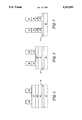
- FIG. 1 shows a cross-sectioned oxide/silicide/poly sandwich structure with a patterned resist mask layer, prior to the inventive etch.
- FIG. 2 shows a cross-section of said structure after oxide etch.
- FIG. 3 shows a cross-section of said structure after polycide etch.
- a photoresist mask layer 10 is aligned and developed on a sandwich structure of oxide 11, silicide 12, and poly 13 on gate oxide 14 of a silicon wafer substrate 15. Fabrication and masking of this structure are done by methods well known to those skilled in semiconductor design and processing, and hence are not fully disclosed herein.
- the preferred embodiment of the inventive method is well suited to etch a 3,000 angstrom layer 11 of TEOS oxide (an oxide of silicon, derived from tetraethylorthosilicate) on 1,200 angstroms of tungsten silicide 12 on 3,000 angstroms of poly 13.
- the wafer having the masked structure is transferred into the chamber of a Lam 790 parallel plate plasma reactor, having an anodized aluminum cathode, a variable gap, and a 13.56 MHz rf power plasma generator for an inventive process having two steps: oxide etch and polycide etch.
- oxide etch step oxide 11 not protected by resist 10 is exposed to a plasma of about 1.9 W/cm 2 power density at a 0.48 cm gap, in a 2.3 torr atmosphere of 50 sccm C 2 F 6 , 100 sccm He, 40 sccm CF 4 , and 32 sccm CHF 3 .
- sccm denotes standard cubic centimeters per minute
- gap refers to the distance between plasma electrodes, one of which supports the wafer.
- silicide and poly layers 12 and 13 are etched in a plasma of about 0.57 W/cm 2 at a 1.0 cm gap in a 0.325 torr atmosphere of 90 sccm Cl 2 and 70 sccm He. This etch takes a little over 2 minutes, with the entire inventive process taking about 3 minutes.
- the finished structure appears as shown in FIG. 3, with a profile at or near 90° from horizontal, with no bowing or notching.
- plasma power density can range within about 0.18-4.0 W/cm 2
- the gap can vary within about 0.3-0.6 cm, 0.38-0.52 cm being the preferred range
- the pressure can range within about 1.8-3.0 torr, although 2.2-2.4 torr is preferred.
- Gas quantities may vary, as long as at least about 5 sccm He is provided. Providing more CF 4 than CHF 3 makes a cleaner process, but this ratio can be varied if desired.
- the inventive process uses a non-erodible anodized aluminum cathode, which increases the amount of available fluorine radicals.
- a non-erodible anodized aluminum cathode which increases the amount of available fluorine radicals.
- the ratio of CF 4 to CHF 3 must be decreased to minimize fluorine radicals. It was found that this approach does not provide adequate selectivity without an excessive and quick buildup of polymer.
- C 2 F 6 also resolves a "micromasking" problem, in which areas of underlying polycide were not being etched.
- the inventive process includes a high pressure atmosphere in order to produce a faster oxide etch rate.
- High pressure results in a higher fluorine radical flux on the oxide surface.
- the etch rate is increased.
- High pressure and rf power do have drawbacks, however. Although rf induced ion bombardment assists in oxide etch, it also contributes to photoresist erosion, which is undesirable. Further, if rf power is too high, the resist will "burn" or reticulate. Higher pressure makes a thicker atmosphere, scattering ions and gas radicals in the plasma, resulting in more sidewall etching than with a low pressure system.
- the oxide etch step of the inventive method includes an overetch of about 45 seconds to fully clear all residual oxide.
- the C 2 F 6 /CF 4 /CHF 3 gas mixture etches underlying polycide during overetch, the etch continues to be anisotropic because of the sidewall passivation provided by the halocarbon-derived polymer and from the carbon introduced by eroding resist.
- the polycide-to-resist etch rate ratio is approximately 1.8:1.
- plasma power density can range within about 0.18-2.0 W/cm 2
- the gap can vary within about 0.5-2.5 cm, 0.8-1.5 cm being the preferred range
- the pressure can range within about 0.200-0.550 torr, although about 0.300-0.425 torr is preferred.
- Quantities of the gases may vary, as long as at least about 50 sccm He is provided. It is contemplated that SiCl 4 or BCl 3 or a combination thereof might be used to provide additional Cl 2 , if desired.
- the lower pressure of the polycide etch allows for more ion bombardment, which, with resist erosion and the Cl 2 concentration, determines the etch rate and profile of the silicide and poly layers 12 and 13.
- Cl 2 provides the necessary selectivity to the polycide, so that minimal underlying gate oxide 14 is etched. Fluorine can also be used, but Cl 2 is preferred because it provides superior selectivity.
- the resist used must therefore be able to reasonably withstand a chlorine based plasma.
- the preferred embodiment utilizes Hunt's 6512 resist, developed with Hunt's photoresist developer 428. It is realized that other resists, developers, and mask layer compositions can be used as well.
- An additional benefit of the inventive method is the ability to use carbon generated by the resist to help passivate polycide sidewalls, which means that carbon-containing gases do not have to be added to the gas mixture during polycide etch.
- helium is added to improve etch uniformity.
- the pressure, power, and various gas quantities are balanced to produce the fastest etch rates while preserving selectivity.
Landscapes
- Drying Of Semiconductors (AREA)
Abstract
A method to anisotropically etch an oxide/silicide/poly sandwich structure on a silicon wafer substrate in situ, that is, using a single parallel plate plasma reactor chamber and a single inert cathode, with a variable gap between cathode and anode. This method has an oxide etch step that utilizes C2 F6, CF4, CHF3 and an inert carrier gas as the etching atmosphere. The fully etched sandwich structure has a vertical profile at or near 90° from horizontal, with no bowing or notching.
Description
This is a continuation of U.S. patent application Ser. No. 382,403, filed Sep. 20, 1989, now abandoned.
1. Field of the Invention
The present invention relates to etching methods used in the fabrication of integrated electronic circuits on a semiconductor substrate such as silicon, particularly a single-chamber/single-cathode (in situ) method of anisotropically plasma etching a sandwich structure of an oxide, tungsten silicide, and polycrystalline silicon, or equivalent structure.
An electronic circuit is chemically and physically integrated into a substrate such as a silicon wafer by patterning regions in the substrate, and by patterning layers on the substrate. These regions and layers can be conductive, for conductor and resistor fabrication, or insulative, for insulator and capacitor fabrication. They can also be of differing conductivity types, which is essential for transistor and diode fabrication. Degrees of resistance, capacitance, and conductivity are controllable, as are the physical dimensions and locations of the patterned regions and layers, making circuit integration possible. Fabrication can be quite complex and time consuming, and therefore expensive. It is thus a continuing quest of those in the semiconductor fabrication business to reduce fabrication times and costs of such devices in order to increase profits. Any simplified processing step or combination of processes at a single step becomes a competitive advantage.
2. Description of the Related Art
A situation where a process simplification is desirable is in the anisotropic etch of a layer of oxide on a layer of silicide on a layer of poly (also called a oxide/silicide/poly sandwich structure). In this disclosure, "oxide" denotes an oxide of silicon, "silicide" is short for tungsten silicide, and "poly" is shoptalk for polycrystalline silicon. "Polycide" denotes a silicide-over-poly combination. Oxide is an insulator with dielectric properties. Poly is resistive in nature, but is made less resistive when doped with an element having less or more than four valence electrons, or when layered with conductive silicide.
An oxide/silicide/poly sandwich structure presents a difficult etching task, particularly with an additional mask layer of photoresist ("resist"), which must be the case if patterning is desired. The difficulty is due to the distinct differences in the way oxide and polycide are etched, particularly with resist still present on top of the structure.
Both oxide and polycide can be etched using a parallel plate plasma reactor. However, an oxide is typically etched in fluorine deficient fluorocarbon based plasmas, whereas silicide and poly can be etched in fluorine or chlorine based discharges. Reactor cathode materials may also differ: for oxide etch, an erodible cathode such as graphite or silicon is often used to provide a source of carbon or silicon for etch selectivity, whereas for polycide etch, an inert cathode is preferred, especially when utilizing chlorine gas (Cl2) for selectivity. If a single-chamber process were attempted using conventional art to etch an oxide/silicide/poly sandwich structure, the erodible cathode required for oxide etch would be destroyed by the chlorine required for polycide etch. Using conventional methods, the two steps are incompatible.
Oxide etch in general is fairly well understood, given a universal need for a vertical profile. This vertical profile is realized primarily by ion induced reaction with the oxide, coupled with normal incidence of the ions onto the oxide surface. The amount and energy of these ions are primarily controlled by the reactor's rf power and gap. Generally, a fluorocarbon-based gas mixture is introduced at a low pressure into the etch chamber. The exact gas composition is chosen, and an erodible cathode is used to scavenge excessive fluorine radicals so that the fluorine-to-carbon ratio is near, but not beyond, the so-called polymerization point. Under these conditions, when a plasma is ignited, the fluorocarbons are dissociated and release fluorine radicals and CFX species. Although fluorine radicals etch oxide, they do so very slowly: the primary etchant for oxide is considered to be the CFX species. Some of these species diffuse to the oxide surface where, with the assistance of ion bombardment, they react with the oxide and release volatile byproducts SiF4, CO, and CO2. In addition, some of the CFX species react with each other to form fluorocarbon polymers. Polymer that forms on horizontal surfaces is removed by vertical ion bombardment. Polymer that forms on vertical sidewalls is not significantly degraded by the bombardment, and actually serves a useful purpose by protecting the sidewalls from attack by the etchant species. This sidewall protection enables the achievement of vertical profiles, adjustable by varying the fluorine-to-carbon ratio. As the cathode is eroded, the quantity of available fluorine radicals is reduced. Therefore, a polymer-producing gas such as CHF3 is balanced against a fluorine producing gas such as CF4 to provide proper selectivity, with assistance to sidewall protection.
Two methods are presently used to etch an oxide/silicide/poly sandwich structure. Both methods use separate reactors: one for oxide etch, and one for polycide etch. The first method involves etching the oxide in an oxide etch reactor, using an erodible cathode. After oxide etch, the resist is removed from the wafer. Silicide and poly are then etched in a poly etch reactor, using an inert cathode. Both etches are anisotropic.
The second method uses the same principles as the first, except that there are two reactors in one machine. The two reactors are configured as separate oxide and polycide reactors having a common vacuum transfer area, so that a wafer can be transferred in a vacuum from the oxide reactor to the polycide reactor, thus minimizing additional handling. The resist is generally not removed prior to polycide etch in this method. This is sometimes referred to as "in situ" since the wafers never leave the vacuum of one machine. However, they are etched in two different etch chambers and are not truly in situ in the sense of this disclosure.
It would be of great advantage to etch oxide and polycide truly "in situ", that is, in one reactor chamber, with a single cathode.
An object of the present invention is to provide a method of anisotropically etching an oxide/silicide/poly sandwich structure in situ. Other objects of the invention are a fast processing time, and improved process yield and cleanliness.
In summary, the inventive process is as follows. A wafer having the sandwich structure described above, coated with a mask layer of resist, is transferred into the chamber of a parallel plate plasma reactor, having an anodized aluminum cathode and a variable gap, for two steps: oxide etch and polycide etch. In the oxide etch step, oxide not protected by resist is exposed to a plasma of about 1.9 W/cm2 power density at a 0.48 cm gap, in a 2.3 torr atmosphere of 50 sccm C2 F6, 100 sccm He, 40 sccm CF4, and 32 sccm CHF3. Immediately after the oxide etch step, in the same chamber and using the same cathode, silicide and poly layers are etched in a plasma of about 0.57 W/cm2 at a 1.0 cm gap in a 0.325 torr atmosphere of 90 sccm Cl2 and 70 sccm He. The finished structure has a vertical profile at or near 90° from horizontal, with no bowing or notching. The entire inventive process takes about 3 minutes.
FIG. 1 shows a cross-sectioned oxide/silicide/poly sandwich structure with a patterned resist mask layer, prior to the inventive etch.
FIG. 2 shows a cross-section of said structure after oxide etch.
FIG. 3 shows a cross-section of said structure after polycide etch.
As illustrated in FIG. 1, a photoresist mask layer 10 is aligned and developed on a sandwich structure of oxide 11, silicide 12, and poly 13 on gate oxide 14 of a silicon wafer substrate 15. Fabrication and masking of this structure are done by methods well known to those skilled in semiconductor design and processing, and hence are not fully disclosed herein. The preferred embodiment of the inventive method is well suited to etch a 3,000 angstrom layer 11 of TEOS oxide (an oxide of silicon, derived from tetraethylorthosilicate) on 1,200 angstroms of tungsten silicide 12 on 3,000 angstroms of poly 13.
The wafer having the masked structure is transferred into the chamber of a Lam 790 parallel plate plasma reactor, having an anodized aluminum cathode, a variable gap, and a 13.56 MHz rf power plasma generator for an inventive process having two steps: oxide etch and polycide etch. In the oxide etch step, oxide 11 not protected by resist 10 is exposed to a plasma of about 1.9 W/cm2 power density at a 0.48 cm gap, in a 2.3 torr atmosphere of 50 sccm C2 F6, 100 sccm He, 40 sccm CF4, and 32 sccm CHF3. In this disclosure, "sccm" denotes standard cubic centimeters per minute, and "gap" refers to the distance between plasma electrodes, one of which supports the wafer. After the oxide etch step, which takes under a minute, the structure appears as shown in FIG. 2.
Immediately after the oxide etch step, in the same chamber and using the same cathode, silicide and poly layers 12 and 13 are etched in a plasma of about 0.57 W/cm2 at a 1.0 cm gap in a 0.325 torr atmosphere of 90 sccm Cl2 and 70 sccm He. This etch takes a little over 2 minutes, with the entire inventive process taking about 3 minutes. The finished structure appears as shown in FIG. 3, with a profile at or near 90° from horizontal, with no bowing or notching.
Details of the oxide etch step are now provided. Although preferred parameter values are stated above, plasma power density can range within about 0.18-4.0 W/cm2, the gap can vary within about 0.3-0.6 cm, 0.38-0.52 cm being the preferred range, and the pressure can range within about 1.8-3.0 torr, although 2.2-2.4 torr is preferred. Gas quantities may vary, as long as at least about 5 sccm He is provided. Providing more CF4 than CHF3 makes a cleaner process, but this ratio can be varied if desired.
The inventive process uses a non-erodible anodized aluminum cathode, which increases the amount of available fluorine radicals. According to conventional thought, in order to maintain the same oxide-to-polycide selectivity as the prior art, the ratio of CF4 to CHF3 must be decreased to minimize fluorine radicals. It was found that this approach does not provide adequate selectivity without an excessive and quick buildup of polymer. This was solved by adding C2 F6 to the chamber atmosphere as the predominant gas, which provides more CFX species and relatively few fluorine radicals, resulting in acceptable selectivity without excessive polymer buildup. C2 F6 also resolves a "micromasking" problem, in which areas of underlying polycide were not being etched. Although the cause is unclear, it is speculated that the CFX species reacted with the tungsten silicide, forming a polymer layer which interfered with subsequent polycide etching. C2 F6 evidently produces a polymer without this affinity for tungsten silicide, thereby eliminating micromasking.
The inventive process includes a high pressure atmosphere in order to produce a faster oxide etch rate. High pressure results in a higher fluorine radical flux on the oxide surface. When combined with high rf power, the etch rate is increased. High pressure and rf power do have drawbacks, however. Although rf induced ion bombardment assists in oxide etch, it also contributes to photoresist erosion, which is undesirable. Further, if rf power is too high, the resist will "burn" or reticulate. Higher pressure makes a thicker atmosphere, scattering ions and gas radicals in the plasma, resulting in more sidewall etching than with a low pressure system.
The oxide etch step of the inventive method includes an overetch of about 45 seconds to fully clear all residual oxide. Although the C2 F6 /CF4 /CHF3 gas mixture etches underlying polycide during overetch, the etch continues to be anisotropic because of the sidewall passivation provided by the halocarbon-derived polymer and from the carbon introduced by eroding resist. After oxide has been cleared, the polycide-to-resist etch rate ratio is approximately 1.8:1.
Polycide etch step details are now provided. Although preferred parameter values have been stated, plasma power density can range within about 0.18-2.0 W/cm2, the gap can vary within about 0.5-2.5 cm, 0.8-1.5 cm being the preferred range, and the pressure can range within about 0.200-0.550 torr, although about 0.300-0.425 torr is preferred. Quantities of the gases may vary, as long as at least about 50 sccm He is provided. It is contemplated that SiCl4 or BCl3 or a combination thereof might be used to provide additional Cl2, if desired.
The lower pressure of the polycide etch allows for more ion bombardment, which, with resist erosion and the Cl2 concentration, determines the etch rate and profile of the silicide and poly layers 12 and 13. Cl2 provides the necessary selectivity to the polycide, so that minimal underlying gate oxide 14 is etched. Fluorine can also be used, but Cl2 is preferred because it provides superior selectivity. The resist used must therefore be able to reasonably withstand a chlorine based plasma. The preferred embodiment utilizes Hunt's 6512 resist, developed with Hunt's photoresist developer 428. It is realized that other resists, developers, and mask layer compositions can be used as well.
An additional benefit of the inventive method is the ability to use carbon generated by the resist to help passivate polycide sidewalls, which means that carbon-containing gases do not have to be added to the gas mixture during polycide etch.
There is an upper rf power limit that can be safely used before the poly-to-gate oxide selectivity is reduced to the point where the poly cannot be completely etched without removing all of the exposed gate oxide. The inventive process provides a selectivity of approximately 13:1. Variations in the chlorine flow and total pressure do not significantly change this selectivity, although an increase in rf power reduces it.
In both of the inventive steps, helium is added to improve etch uniformity. The pressure, power, and various gas quantities are balanced to produce the fastest etch rates while preserving selectivity.
Clearly, in view of the above disclosure, other embodiments of this invention will present themselves to those of ordinary skill in semiconductor processing, such as applying the invention to other kinds of masking layers, oxide, silicide, and poly, and varying thickness and doping of each layer etched. Since the inventive process includes one step for polycide etch, a simple oxide/poly structure can be etched instead of an oxide/silicide/poly structure, without materially altering the process. It is also conceivable that plasma power density and gap may be varied, gas quantities adjusted, similar gases substituted, or some other inert material used for the cathode, to achieve same or similar results. Gas quantities may also be changed while preserving essentially similar ratios of one gas to another. Another make of reactor might also be chosen. These variations and others are intended to be circumscribed by these claims.
Claims (6)
1. A method of anisotropically etching dielectric layer on a substrate, comprising the steps of:
a) providing a parallel plate plasma etch reactor, having a first electrode whereupon the substrate is mounted, and having a second electrode that is non-erodible by plasma;
b) providing an atmosphere within said reactor, consisting essentially of C2 F6, CHF3, CF4, and an inert carrier gas, whereby said atmosphere contains more C2 F6 than CF4, and more CF4 than CHF3 ;
c) exposing the dielectric layer to a plasma maintained in said atmosphere.
2. The method of claim 1, wherein:
a) said atmosphere has a pressure of approximately 2.3 torr and includes approximately 50 sccm C2 F6, approximately 32 sccm CHF3, approximately 40 sccm CF4, and approximately 100 sccm He as its inert carrier gas;
b) a power density of said plasma is approximately 1.9 W/cm2 ;
c) a gap of approximately 0.48 cm exists between said first and second electrodes; and
d) said non-erodible second electrode is anodized aluminum.
3. The method of claim 1, wherein:
a) said atmosphere has a pressure of approximately 1.8 to 3.0 torr;
b) a power density of said plasma is approximately 0.18 to 4.0 W/cm2 ;
c) a gap of approximately 0.3 to 0.6 cm exists between said first and second electrodes; and
d) said non-erodible second electrode is anodized aluminum.
4. The method of claim 1, wherein:
a) said atmosphere has a pressure of approximately 2.2 to 2.4 torr;
b) a power density of said plasma approximately 0.18 to 4.0 W/cm2 ;
c) a gap of approximately 0.38 to 0.52 cm exists between said first and second electrodes; and
d) said non-erodible second electrode is anodized aluminum.
5. The method of claim 1, wherein said atmosphere includes at least approximately 5 sccm He as its inert carrier gas.
6. A method of anisotropically etching a dielectric layer on a substrate wafer, comprising the steps of:
a) providing a parallel plate plasma etch reactor, having a first electrode whereupon the substrate wafer is mounted, and having a second electrode that is non-erodible by plasma;
b) providing an atmosphere within said reactor, consisting essentially of C2 F6, CF4, CHF3 and an inert carrier gas, said atmosphere containing more C2 F6 than CF4 and more CF4 than CHF3, and having a pressure of approximately 1.8 to 3.0 torr;
c) performing a plasma etch step in the reactor, with C2 F6 in the atmosphere as the predominant gas, thereby providing more CFX species than F radials and relatively few fluorine radicals, and reducing micromasking on the wafer; and
d) exposing the dielectric layer to a plasma having a power density of approximately 0.18 to 4.0 W/cm2.
Priority Applications (7)
| Application Number | Priority Date | Filing Date | Title |
|---|---|---|---|
| US07/574,578 US5201993A (en) | 1989-07-20 | 1990-08-27 | Anisotropic etch method |
| US08/603,573 US5958801A (en) | 1989-07-20 | 1996-02-20 | Anisotropic etch method |
| US08/909,229 US6133156A (en) | 1989-07-20 | 1997-08-11 | Anisotropic etch method |
| US09/571,523 US6461976B1 (en) | 1989-07-20 | 2000-05-16 | Anisotropic etch method |
| US10/213,170 US7375036B2 (en) | 1989-07-20 | 2002-08-05 | Anisotropic etch method |
| US10/219,141 US6686295B2 (en) | 1989-07-20 | 2002-08-14 | Anisotropic etch method |
| US10/928,374 US20050026440A1 (en) | 1989-07-20 | 2004-08-27 | Anisotropic etch method |
Applications Claiming Priority (2)
| Application Number | Priority Date | Filing Date | Title |
|---|---|---|---|
| US07/382,403 US5271799A (en) | 1989-07-20 | 1989-07-20 | Anisotropic etch method |
| US07/574,578 US5201993A (en) | 1989-07-20 | 1990-08-27 | Anisotropic etch method |
Related Parent Applications (1)
| Application Number | Title | Priority Date | Filing Date |
|---|---|---|---|
| US07/382,403 Continuation US5271799A (en) | 1989-07-20 | 1989-07-20 | Anisotropic etch method |
Related Child Applications (2)
| Application Number | Title | Priority Date | Filing Date |
|---|---|---|---|
| US87743592A Division | 1989-07-20 | 1992-04-30 | |
| US19413494A Division | 1989-07-20 | 1994-02-08 |
Publications (1)
| Publication Number | Publication Date |
|---|---|
| US5201993A true US5201993A (en) | 1993-04-13 |
Family
ID=27009746
Family Applications (7)
| Application Number | Title | Priority Date | Filing Date |
|---|---|---|---|
| US07/574,578 Expired - Lifetime US5201993A (en) | 1989-07-20 | 1990-08-27 | Anisotropic etch method |
| US08/603,573 Expired - Fee Related US5958801A (en) | 1989-07-20 | 1996-02-20 | Anisotropic etch method |
| US08/909,229 Expired - Fee Related US6133156A (en) | 1989-07-20 | 1997-08-11 | Anisotropic etch method |
| US09/571,523 Expired - Fee Related US6461976B1 (en) | 1989-07-20 | 2000-05-16 | Anisotropic etch method |
| US10/213,170 Expired - Fee Related US7375036B2 (en) | 1989-07-20 | 2002-08-05 | Anisotropic etch method |
| US10/219,141 Expired - Fee Related US6686295B2 (en) | 1989-07-20 | 2002-08-14 | Anisotropic etch method |
| US10/928,374 Abandoned US20050026440A1 (en) | 1989-07-20 | 2004-08-27 | Anisotropic etch method |
Family Applications After (6)
| Application Number | Title | Priority Date | Filing Date |
|---|---|---|---|
| US08/603,573 Expired - Fee Related US5958801A (en) | 1989-07-20 | 1996-02-20 | Anisotropic etch method |
| US08/909,229 Expired - Fee Related US6133156A (en) | 1989-07-20 | 1997-08-11 | Anisotropic etch method |
| US09/571,523 Expired - Fee Related US6461976B1 (en) | 1989-07-20 | 2000-05-16 | Anisotropic etch method |
| US10/213,170 Expired - Fee Related US7375036B2 (en) | 1989-07-20 | 2002-08-05 | Anisotropic etch method |
| US10/219,141 Expired - Fee Related US6686295B2 (en) | 1989-07-20 | 2002-08-14 | Anisotropic etch method |
| US10/928,374 Abandoned US20050026440A1 (en) | 1989-07-20 | 2004-08-27 | Anisotropic etch method |
Country Status (1)
| Country | Link |
|---|---|
| US (7) | US5201993A (en) |
Cited By (24)
| Publication number | Priority date | Publication date | Assignee | Title |
|---|---|---|---|---|
| US5324689A (en) * | 1993-07-28 | 1994-06-28 | Taiwan Semiconductor Manufacturing Company | Critical dimension control with a planarized underlayer |
| US5346586A (en) * | 1992-12-23 | 1994-09-13 | Micron Semiconductor, Inc. | Method for selectively etching polysilicon to gate oxide using an insitu ozone photoresist strip |
| EP0649166A3 (en) * | 1993-10-13 | 1995-07-26 | At & T Corp | Method for manufacturing transistor doors. |
| US5563098A (en) * | 1995-04-10 | 1996-10-08 | Taiwan Semiconductor Manufacturing Company | Buried contact oxide etch with poly mask procedure |
| US5691246A (en) * | 1993-05-13 | 1997-11-25 | Micron Technology, Inc. | In situ etch process for insulating and conductive materials |
| US5827762A (en) * | 1997-05-02 | 1998-10-27 | National Semiconductor Corporation | Method for forming buried interconnect structue having stability at high temperatures |
| US5843845A (en) * | 1995-12-27 | 1998-12-01 | Lg Semicon Co., Ltd. | Method for forming sloped contact hole for semiconductor device |
| US5856239A (en) * | 1997-05-02 | 1999-01-05 | National Semiconductor Corporaton | Tungsten silicide/ tungsten polycide anisotropic dry etch process |
| US5958801A (en) * | 1989-07-20 | 1999-09-28 | Micron Technology, Inc. | Anisotropic etch method |
| US5990009A (en) * | 1996-11-19 | 1999-11-23 | Integrated Device Technology, Inc. | Maximization of low dielectric constant material between interconnect traces of a semiconductor circuit |
| US6025273A (en) * | 1998-04-06 | 2000-02-15 | Taiwan Semiconductor Manufacturing Company, Ltd. | Method for etching reliable small contact holes with improved profiles for semiconductor integrated circuits using a carbon doped hard mask |
| US6051504A (en) * | 1997-08-15 | 2000-04-18 | International Business Machines Corporation | Anisotropic and selective nitride etch process for high aspect ratio features in high density plasma |
| US6083815A (en) * | 1998-04-27 | 2000-07-04 | Taiwan Semiconductor Manufacturing Company | Method of gate etching with thin gate oxide |
| US6159833A (en) * | 1999-09-08 | 2000-12-12 | United Microelectronics Corp. | Method of forming a contact hole in a semiconductor wafer |
| US6159860A (en) * | 1998-07-17 | 2000-12-12 | Advanced Micro Devices, Inc. | Method for etching layers on a semiconductor wafer in a single etching chamber |
| EP1195802A1 (en) * | 2000-10-06 | 2002-04-10 | Semiconductor300 GmbH & Co KG | Process for forming conductor lines on a semiconductor product |
| US6440762B1 (en) | 1998-10-06 | 2002-08-27 | Micron Technology, Inc. | Low temperature process for sharpening tapered silicon structures |
| US6461529B1 (en) | 1999-04-26 | 2002-10-08 | International Business Machines Corporation | Anisotropic nitride etch process with high selectivity to oxide and photoresist layers in a damascene etch scheme |
| US6605541B1 (en) * | 1998-05-07 | 2003-08-12 | Advanced Micro Devices, Inc. | Pitch reduction using a set of offset masks |
| US6686292B1 (en) | 1998-12-28 | 2004-02-03 | Taiwan Semiconductor Manufacturing Company | Plasma etch method for forming uniform linewidth residue free patterned composite silicon containing dielectric layer/silicon stack layer |
| US20040030364A1 (en) * | 2001-01-04 | 2004-02-12 | Cardiac Pacemakers, Inc. | System and method for removing narrowband noise |
| WO2004042771A3 (en) * | 2002-10-31 | 2004-08-19 | Applied Materials Inc | Method of etching a silicon-containing dielectric material |
| US20090104776A1 (en) * | 2007-10-18 | 2009-04-23 | International Business Machines Corporation | Methods for forming nested and isolated lines in semiconductor devices |
| US20090314435A1 (en) * | 2001-06-01 | 2009-12-24 | Tokyo Electron Limited | Plasma processing unit |
Families Citing this family (19)
| Publication number | Priority date | Publication date | Assignee | Title |
|---|---|---|---|---|
| US6117793A (en) * | 1998-09-03 | 2000-09-12 | Micron Technology, Inc. | Using silicide cap as an etch stop for multilayer metal process and structures so formed |
| WO2000052749A1 (en) | 1999-03-05 | 2000-09-08 | Applied Materials, Inc. | Method for enhancing etching of titanium silicide |
| US6300251B1 (en) * | 2000-02-10 | 2001-10-09 | Chartered Semiconductor Manufacturing Ltd. | Repeatable end point method for anisotropic etch of inorganic buried anti-reflective coating layer over silicon |
| US20030010354A1 (en) * | 2000-03-27 | 2003-01-16 | Applied Materials, Inc. | Fluorine process for cleaning semiconductor process chamber |
| US6500356B2 (en) * | 2000-03-27 | 2002-12-31 | Applied Materials, Inc. | Selectively etching silicon using fluorine without plasma |
| US6225234B1 (en) * | 2000-03-30 | 2001-05-01 | Lam Research Corporation | In situ and ex situ hardmask process for STI with oxide collar application |
| US6387820B1 (en) * | 2000-09-19 | 2002-05-14 | Advanced Micro Devices, Inc. | BC13/AR chemistry for metal overetching on a high density plasma etcher |
| US6843258B2 (en) * | 2000-12-19 | 2005-01-18 | Applied Materials, Inc. | On-site cleaning gas generation for process chamber cleaning |
| US6784110B2 (en) | 2002-10-01 | 2004-08-31 | Jianping Wen | Method of etching shaped features on a substrate |
| US20040191697A1 (en) * | 2003-03-24 | 2004-09-30 | Communications Research Laboratory | Method for processing a niobium type thin film and method for manufacturing a superconducting integrated circuit |
| US20050236366A1 (en) * | 2004-04-27 | 2005-10-27 | Taiwan Semiconductor Manufacturing Co. | Use of C2F6 gas to gain vertical profile in high dosage implanted poly film |
| JP4801553B2 (en) * | 2006-09-28 | 2011-10-26 | 東京エレクトロン株式会社 | Etching method and semiconductor device manufacturing method |
| US7988203B2 (en) * | 2007-09-05 | 2011-08-02 | Sewer Tap Inc. | Minimal penetration lateral pipe connection assembly |
| DE102007045734B3 (en) * | 2007-09-25 | 2008-11-13 | Qimonda Ag | Method for structuring of isolating material and semiconducting material in semiconductor elements for production of integrated circuit, involves partial clearing of semiconducting material |
| CN101952944B (en) * | 2007-11-21 | 2013-01-02 | 朗姆研究公司 | Method and apparatus for controlling etching microloading of tungsten-containing layer |
| US8137036B2 (en) * | 2007-12-28 | 2012-03-20 | Sewer Tap Inc. | Coring tool alignment system |
| US8770897B2 (en) * | 2009-11-04 | 2014-07-08 | Advanced Drainage Systems, Inc. | Coring tool alignment assembly |
| US8133814B1 (en) * | 2010-12-03 | 2012-03-13 | Globalfoundries Inc. | Etch methods for semiconductor device fabrication |
| US9966312B2 (en) * | 2015-08-25 | 2018-05-08 | Tokyo Electron Limited | Method for etching a silicon-containing substrate |
Citations (12)
| Publication number | Priority date | Publication date | Assignee | Title |
|---|---|---|---|---|
| US4340462A (en) * | 1981-02-13 | 1982-07-20 | Lam Research Corporation | Adjustable electrode plasma processing chamber |
| US4414057A (en) * | 1982-12-03 | 1983-11-08 | Inmos Corporation | Anisotropic silicide etching process |
| US4460435A (en) * | 1983-12-19 | 1984-07-17 | Rca Corporation | Patterning of submicrometer metal silicide structures |
| US4473436A (en) * | 1982-05-05 | 1984-09-25 | Siemens Aktiengesellschaft | Method of producing structures from double layers of metal silicide and polysilicon on integrated circuit substrates by RIE utilizing SF6 and Cl2 |
| US4659426A (en) * | 1985-05-03 | 1987-04-21 | Texas Instruments Incorporated | Plasma etching of refractory metals and their silicides |
| US4680086A (en) * | 1986-03-20 | 1987-07-14 | Motorola, Inc. | Dry etching of multi-layer structures |
| US4726879A (en) * | 1986-09-08 | 1988-02-23 | International Business Machines Corporation | RIE process for etching silicon isolation trenches and polycides with vertical surfaces |
| US4778563A (en) * | 1987-03-26 | 1988-10-18 | Applied Materials, Inc. | Materials and methods for etching tungsten polycides using silicide as a mask |
| US4812418A (en) * | 1987-11-27 | 1989-03-14 | Motorola, Inc. | Micron and submicron patterning without using a lithographic mask having submicron dimensions |
| US4828649A (en) * | 1987-07-16 | 1989-05-09 | Texas Instruments Incorporated | Method for etching an aluminum film doped with silicon |
| US4869781A (en) * | 1987-10-30 | 1989-09-26 | International Business Machines Corporation | Method for fabricating a semiconductor integrated circuit structure having a submicrometer length device element |
| US4894693A (en) * | 1985-05-01 | 1990-01-16 | Tigelaar Howard L | Single-polysilicon dram device and process |
Family Cites Families (20)
| Publication number | Priority date | Publication date | Assignee | Title |
|---|---|---|---|---|
| US4214946A (en) * | 1979-02-21 | 1980-07-29 | International Business Machines Corporation | Selective reactive ion etching of polysilicon against SiO2 utilizing SF6 -Cl2 -inert gas etchant |
| JPS56148833A (en) * | 1980-04-22 | 1981-11-18 | Toshiba Corp | Plasma etching method |
| US4324611A (en) * | 1980-06-26 | 1982-04-13 | Branson International Plasma Corporation | Process and gas mixture for etching silicon dioxide and silicon nitride |
| US4400865A (en) * | 1980-07-08 | 1983-08-30 | International Business Machines Corporation | Self-aligned metal process for integrated circuit metallization |
| US4937643A (en) * | 1981-05-22 | 1990-06-26 | American Telephone And Telegraph Company | Devices having tantalum silicide structures |
| US4419201A (en) * | 1981-08-24 | 1983-12-06 | Bell Telephone Laboratories, Incorporated | Apparatus and method for plasma-assisted etching of wafers |
| JPS58122730A (en) * | 1982-01-14 | 1983-07-21 | Toshiba Corp | Dry etching method |
| US4418094A (en) * | 1982-03-02 | 1983-11-29 | Texas Instruments Incorporated | Vertical-etch direct moat isolation process |
| DE3272083D1 (en) * | 1982-03-31 | 1986-08-28 | Ibm Deutschland | Reactor for reactive ion etching, and etching process |
| US4502915B1 (en) * | 1984-01-23 | 1998-11-03 | Texas Instruments Inc | Two-step plasma process for selective anisotropic etching of polycrystalline silicon without leaving residue |
| US4528066A (en) * | 1984-07-06 | 1985-07-09 | Ibm Corporation | Selective anisotropic reactive ion etching process for polysilicide composite structures |
| JPS621887A (en) * | 1985-06-26 | 1987-01-07 | Matsushita Electric Ind Co Ltd | Dry etching apparatus |
| US4818334A (en) * | 1988-03-15 | 1989-04-04 | General Electric Company | Method of etching a layer including polysilicon |
| GB2219434A (en) * | 1988-06-06 | 1989-12-06 | Philips Nv | A method of forming a contact in a semiconductor device |
| US5201993A (en) * | 1989-07-20 | 1993-04-13 | Micron Technology, Inc. | Anisotropic etch method |
| US5271799A (en) * | 1989-07-20 | 1993-12-21 | Micron Technology, Inc. | Anisotropic etch method |
| US4971655A (en) * | 1989-12-26 | 1990-11-20 | Micron Technology, Inc. | Protection of a refractory metal silicide during high-temperature processing using a dual-layer cap of silicon dioxide and silicon nitride |
| US5169487A (en) * | 1990-08-27 | 1992-12-08 | Micron Technology, Inc. | Anisotropic etch method |
| US5691246A (en) * | 1993-05-13 | 1997-11-25 | Micron Technology, Inc. | In situ etch process for insulating and conductive materials |
| US5889749A (en) * | 1995-04-27 | 1999-03-30 | Fuji Photo Optical Co., Ltd. | Optical pickup apparatus |
-
1990
- 1990-08-27 US US07/574,578 patent/US5201993A/en not_active Expired - Lifetime
-
1996
- 1996-02-20 US US08/603,573 patent/US5958801A/en not_active Expired - Fee Related
-
1997
- 1997-08-11 US US08/909,229 patent/US6133156A/en not_active Expired - Fee Related
-
2000
- 2000-05-16 US US09/571,523 patent/US6461976B1/en not_active Expired - Fee Related
-
2002
- 2002-08-05 US US10/213,170 patent/US7375036B2/en not_active Expired - Fee Related
- 2002-08-14 US US10/219,141 patent/US6686295B2/en not_active Expired - Fee Related
-
2004
- 2004-08-27 US US10/928,374 patent/US20050026440A1/en not_active Abandoned
Patent Citations (12)
| Publication number | Priority date | Publication date | Assignee | Title |
|---|---|---|---|---|
| US4340462A (en) * | 1981-02-13 | 1982-07-20 | Lam Research Corporation | Adjustable electrode plasma processing chamber |
| US4473436A (en) * | 1982-05-05 | 1984-09-25 | Siemens Aktiengesellschaft | Method of producing structures from double layers of metal silicide and polysilicon on integrated circuit substrates by RIE utilizing SF6 and Cl2 |
| US4414057A (en) * | 1982-12-03 | 1983-11-08 | Inmos Corporation | Anisotropic silicide etching process |
| US4460435A (en) * | 1983-12-19 | 1984-07-17 | Rca Corporation | Patterning of submicrometer metal silicide structures |
| US4894693A (en) * | 1985-05-01 | 1990-01-16 | Tigelaar Howard L | Single-polysilicon dram device and process |
| US4659426A (en) * | 1985-05-03 | 1987-04-21 | Texas Instruments Incorporated | Plasma etching of refractory metals and their silicides |
| US4680086A (en) * | 1986-03-20 | 1987-07-14 | Motorola, Inc. | Dry etching of multi-layer structures |
| US4726879A (en) * | 1986-09-08 | 1988-02-23 | International Business Machines Corporation | RIE process for etching silicon isolation trenches and polycides with vertical surfaces |
| US4778563A (en) * | 1987-03-26 | 1988-10-18 | Applied Materials, Inc. | Materials and methods for etching tungsten polycides using silicide as a mask |
| US4828649A (en) * | 1987-07-16 | 1989-05-09 | Texas Instruments Incorporated | Method for etching an aluminum film doped with silicon |
| US4869781A (en) * | 1987-10-30 | 1989-09-26 | International Business Machines Corporation | Method for fabricating a semiconductor integrated circuit structure having a submicrometer length device element |
| US4812418A (en) * | 1987-11-27 | 1989-03-14 | Motorola, Inc. | Micron and submicron patterning without using a lithographic mask having submicron dimensions |
Cited By (33)
| Publication number | Priority date | Publication date | Assignee | Title |
|---|---|---|---|---|
| US6133156A (en) * | 1989-07-20 | 2000-10-17 | Micron Technology, Inc, | Anisotropic etch method |
| US6686295B2 (en) | 1989-07-20 | 2004-02-03 | Micron Technology, Inc. | Anisotropic etch method |
| US7375036B2 (en) | 1989-07-20 | 2008-05-20 | Micron Technology, Inc | Anisotropic etch method |
| US20050026440A1 (en) * | 1989-07-20 | 2005-02-03 | Langley Rod C. | Anisotropic etch method |
| US5958801A (en) * | 1989-07-20 | 1999-09-28 | Micron Technology, Inc. | Anisotropic etch method |
| US6461976B1 (en) | 1989-07-20 | 2002-10-08 | Micron Technology, Inc. | Anisotropic etch method |
| US5346586A (en) * | 1992-12-23 | 1994-09-13 | Micron Semiconductor, Inc. | Method for selectively etching polysilicon to gate oxide using an insitu ozone photoresist strip |
| US5691246A (en) * | 1993-05-13 | 1997-11-25 | Micron Technology, Inc. | In situ etch process for insulating and conductive materials |
| US5899749A (en) * | 1993-05-13 | 1999-05-04 | Micron Technology, Inc. | In situ etch process for insulating and conductive materials |
| US5324689A (en) * | 1993-07-28 | 1994-06-28 | Taiwan Semiconductor Manufacturing Company | Critical dimension control with a planarized underlayer |
| EP0649166A3 (en) * | 1993-10-13 | 1995-07-26 | At & T Corp | Method for manufacturing transistor doors. |
| US5563098A (en) * | 1995-04-10 | 1996-10-08 | Taiwan Semiconductor Manufacturing Company | Buried contact oxide etch with poly mask procedure |
| US5843845A (en) * | 1995-12-27 | 1998-12-01 | Lg Semicon Co., Ltd. | Method for forming sloped contact hole for semiconductor device |
| US5990009A (en) * | 1996-11-19 | 1999-11-23 | Integrated Device Technology, Inc. | Maximization of low dielectric constant material between interconnect traces of a semiconductor circuit |
| US5856239A (en) * | 1997-05-02 | 1999-01-05 | National Semiconductor Corporaton | Tungsten silicide/ tungsten polycide anisotropic dry etch process |
| US5827762A (en) * | 1997-05-02 | 1998-10-27 | National Semiconductor Corporation | Method for forming buried interconnect structue having stability at high temperatures |
| US6051504A (en) * | 1997-08-15 | 2000-04-18 | International Business Machines Corporation | Anisotropic and selective nitride etch process for high aspect ratio features in high density plasma |
| US6025273A (en) * | 1998-04-06 | 2000-02-15 | Taiwan Semiconductor Manufacturing Company, Ltd. | Method for etching reliable small contact holes with improved profiles for semiconductor integrated circuits using a carbon doped hard mask |
| US6083815A (en) * | 1998-04-27 | 2000-07-04 | Taiwan Semiconductor Manufacturing Company | Method of gate etching with thin gate oxide |
| US6605541B1 (en) * | 1998-05-07 | 2003-08-12 | Advanced Micro Devices, Inc. | Pitch reduction using a set of offset masks |
| US6159860A (en) * | 1998-07-17 | 2000-12-12 | Advanced Micro Devices, Inc. | Method for etching layers on a semiconductor wafer in a single etching chamber |
| US6440762B1 (en) | 1998-10-06 | 2002-08-27 | Micron Technology, Inc. | Low temperature process for sharpening tapered silicon structures |
| US6686292B1 (en) | 1998-12-28 | 2004-02-03 | Taiwan Semiconductor Manufacturing Company | Plasma etch method for forming uniform linewidth residue free patterned composite silicon containing dielectric layer/silicon stack layer |
| US6461529B1 (en) | 1999-04-26 | 2002-10-08 | International Business Machines Corporation | Anisotropic nitride etch process with high selectivity to oxide and photoresist layers in a damascene etch scheme |
| US6159833A (en) * | 1999-09-08 | 2000-12-12 | United Microelectronics Corp. | Method of forming a contact hole in a semiconductor wafer |
| WO2002029880A1 (en) * | 2000-10-06 | 2002-04-11 | Infineon Technologies Sc300 Gmbh & Co. Kg | Process for forming conductor lines on a semiconductor product |
| EP1195802A1 (en) * | 2000-10-06 | 2002-04-10 | Semiconductor300 GmbH & Co KG | Process for forming conductor lines on a semiconductor product |
| US20040030364A1 (en) * | 2001-01-04 | 2004-02-12 | Cardiac Pacemakers, Inc. | System and method for removing narrowband noise |
| US20090314435A1 (en) * | 2001-06-01 | 2009-12-24 | Tokyo Electron Limited | Plasma processing unit |
| WO2004042771A3 (en) * | 2002-10-31 | 2004-08-19 | Applied Materials Inc | Method of etching a silicon-containing dielectric material |
| US20070010099A1 (en) * | 2002-10-31 | 2007-01-11 | Applied Materials, Inc. | Method of pattern etching a silicon-containing hard mask |
| US7504338B2 (en) | 2002-10-31 | 2009-03-17 | Applied Materials, Inc. | Method of pattern etching a silicon-containing hard mask |
| US20090104776A1 (en) * | 2007-10-18 | 2009-04-23 | International Business Machines Corporation | Methods for forming nested and isolated lines in semiconductor devices |
Also Published As
| Publication number | Publication date |
|---|---|
| US20020192973A1 (en) | 2002-12-19 |
| US6461976B1 (en) | 2002-10-08 |
| US6686295B2 (en) | 2004-02-03 |
| US5958801A (en) | 1999-09-28 |
| US6133156A (en) | 2000-10-17 |
| US7375036B2 (en) | 2008-05-20 |
| US20050026440A1 (en) | 2005-02-03 |
| US20020185470A1 (en) | 2002-12-12 |
Similar Documents
| Publication | Publication Date | Title |
|---|---|---|
| US5201993A (en) | Anisotropic etch method | |
| US5169487A (en) | Anisotropic etch method | |
| US5094712A (en) | One chamber in-situ etch process for oxide and conductive material | |
| US5256245A (en) | Use of a clean up step to form more vertical profiles of polycrystalline silicon sidewalls during the manufacture of a semiconductor device | |
| US6602434B1 (en) | Process for etching oxide using hexafluorobutadiene or related fluorocarbons and manifesting a wide process window | |
| US4522681A (en) | Method for tapered dry etching | |
| US4310380A (en) | Plasma etching of silicon | |
| US6387287B1 (en) | Process for etching oxide using a hexafluorobutadiene and manifesting a wide process window | |
| US6620733B2 (en) | Use of hydrocarbon addition for the elimination of micromasking during etching of organic low-k dielectrics | |
| US6326307B1 (en) | Plasma pretreatment of photoresist in an oxide etch process | |
| US4528066A (en) | Selective anisotropic reactive ion etching process for polysilicide composite structures | |
| US6841483B2 (en) | Unique process chemistry for etching organic low-k materials | |
| US6284149B1 (en) | High-density plasma etching of carbon-based low-k materials in a integrated circuit | |
| EP1042796B1 (en) | Improved techniques for etching an oxide layer | |
| US4980018A (en) | Plasma etching process for refractory metal vias | |
| US6183655B1 (en) | Tunable process for selectively etching oxide using fluoropropylene and a hydrofluorocarbon | |
| US5691246A (en) | In situ etch process for insulating and conductive materials | |
| US4472237A (en) | Reactive ion etching of tantalum and silicon | |
| US6849193B2 (en) | Highly selective process for etching oxide over nitride using hexafluorobutadiene | |
| US5453156A (en) | Anisotropic polysilicon plasma etch using fluorine gases | |
| US5180464A (en) | Dry etching method | |
| US5167762A (en) | Anisotropic etch method | |
| JPS6252455B2 (en) | ||
| KR20030066673A (en) | Method of etching tungsten or tungsten nitride electrode gates in semiconductor structures | |
| US5651856A (en) | Selective etch process |
Legal Events
| Date | Code | Title | Description |
|---|---|---|---|
| STCF | Information on status: patent grant |
Free format text: PATENTED CASE |
|
| AS | Assignment |
Owner name: MICRON SEMICONDUCTOR, INC., IDAHO Free format text: ASSIGNMENT OF ASSIGNORS INTEREST;ASSIGNOR:MICRON TECHNOLOGY, INC.;REEL/FRAME:006811/0787 Effective date: 19931215 |
|
| FPAY | Fee payment |
Year of fee payment: 4 |
|
| FPAY | Fee payment |
Year of fee payment: 8 |
|
| FPAY | Fee payment |
Year of fee payment: 12 |