EP0211318B1 - Process for selectively filling contact holes made by etching in insulating layers with electrically conductive materials for the manufacture of high-density integrated semiconductor circuits, and apparatus used for this process - Google Patents
Process for selectively filling contact holes made by etching in insulating layers with electrically conductive materials for the manufacture of high-density integrated semiconductor circuits, and apparatus used for this process Download PDFInfo
- Publication number
- EP0211318B1 EP0211318B1 EP86110076A EP86110076A EP0211318B1 EP 0211318 B1 EP0211318 B1 EP 0211318B1 EP 86110076 A EP86110076 A EP 86110076A EP 86110076 A EP86110076 A EP 86110076A EP 0211318 B1 EP0211318 B1 EP 0211318B1
- Authority
- EP
- European Patent Office
- Prior art keywords
- deposition
- process according
- holes
- silicide
- contact holes
- Prior art date
- Legal status (The legal status is an assumption and is not a legal conclusion. Google has not performed a legal analysis and makes no representation as to the accuracy of the status listed.)
- Expired
Links
Images

Classifications
-
- H—ELECTRICITY
- H01—ELECTRIC ELEMENTS
- H01L—SEMICONDUCTOR DEVICES NOT COVERED BY CLASS H10
- H01L21/00—Processes or apparatus adapted for the manufacture or treatment of semiconductor or solid state devices or of parts thereof
- H01L21/70—Manufacture or treatment of devices consisting of a plurality of solid state components formed in or on a common substrate or of parts thereof; Manufacture of integrated circuit devices or of parts thereof
- H01L21/71—Manufacture of specific parts of devices defined in group H01L21/70
- H01L21/768—Applying interconnections to be used for carrying current between separate components within a device comprising conductors and dielectrics
- H01L21/76838—Applying interconnections to be used for carrying current between separate components within a device comprising conductors and dielectrics characterised by the formation and the after-treatment of the conductors
- H01L21/76877—Filling of holes, grooves or trenches, e.g. vias, with conductive material
- H01L21/76879—Filling of holes, grooves or trenches, e.g. vias, with conductive material by selective deposition of conductive material in the vias, e.g. selective C.V.D. on semiconductor material, plating
-
- H—ELECTRICITY
- H01—ELECTRIC ELEMENTS
- H01L—SEMICONDUCTOR DEVICES NOT COVERED BY CLASS H10
- H01L23/00—Details of semiconductor or other solid state devices
- H01L23/52—Arrangements for conducting electric current within the device in operation from one component to another, i.e. interconnections, e.g. wires, lead frames
- H01L23/522—Arrangements for conducting electric current within the device in operation from one component to another, i.e. interconnections, e.g. wires, lead frames including external interconnections consisting of a multilayer structure of conductive and insulating layers inseparably formed on the semiconductor body
- H01L23/532—Arrangements for conducting electric current within the device in operation from one component to another, i.e. interconnections, e.g. wires, lead frames including external interconnections consisting of a multilayer structure of conductive and insulating layers inseparably formed on the semiconductor body characterised by the materials
- H01L23/53204—Conductive materials
- H01L23/53209—Conductive materials based on metals, e.g. alloys, metal silicides
- H01L23/53257—Conductive materials based on metals, e.g. alloys, metal silicides the principal metal being a refractory metal
-
- H—ELECTRICITY
- H01—ELECTRIC ELEMENTS
- H01L—SEMICONDUCTOR DEVICES NOT COVERED BY CLASS H10
- H01L2924/00—Indexing scheme for arrangements or methods for connecting or disconnecting semiconductor or solid-state bodies as covered by H01L24/00
- H01L2924/0001—Technical content checked by a classifier
- H01L2924/0002—Not covered by any one of groups H01L24/00, H01L24/00 and H01L2224/00
Definitions
- the invention relates to a method for the selective filling of contact holes etched in insulation layers or via holes (these are relatively small holes that are produced between the interconnect levels) with metallically conductive materials, such as those used in particular for the production of highly integrated semiconductor circuits for the formation of electrical interconnects on structured ones Semiconductor substrates are required, and an apparatus for performing the method.
- the insulation layer must have a minimum thickness of 0.7 to 1.5 ⁇ m due to circuitry considerations (for example parasitic capacitances), depth / diameter ratios of greater than / equal to 1 occur in the contact holes or via holes.
- the layer thickness of the interconnects on the flanks of the contact hole decreases very significantly (55 to 80% decrease) if the interconnect material, for example aluminum alloys: aluminum-silicon (1%), as previously customary by cathode sputtering (Sputtering) is applied. Since the interconnects are loaded with extremely high current densities (e.g.
- each cross-sectional narrowing causes a local temperature rise, which accelerates undesired material transport (diffusion, reaction) at the interfaces between the different materials in contact. This can also lead to the burnout of an interconnect.
- cavities (15) can form in the contact holes after coating, for example with aluminum-silicon. If an insulation layer is then subsequently deposited, for example as a base for a further aluminum-silicon interconnect level, it is practically not possible to completely fill up the cavity located in the contact hole. Since reactive or corrosive media can sometimes accumulate in this cavity during further production steps, it is necessary for reliable components to specify a contact hole or via hole metallization process in which complete filling takes place.
- Another difficulty with this method is that there is only a poor bond between the selectively growing metal and the side walls of the contact hole consisting of SiO 2 , so that adhesion problems and thus also cavity formation can occur locally.
- the tungsten hexafluoride already causes the approx. 3 nm thick natural oxide skin to be etched.
- this etching step which is a side effect of the coating process, is difficult to control.
- the selective tantalum silicide deposition with tantalum pentachloride as the metal starting compound offers the possibility of carrying out a separate etching step in situ before the coating.
- a defined etching of the natural oxide skin for example with hydrogen fluoride
- the natural oxide skin is very thin and the sum of all contact hole areas is very small compared to the Si0 2 insulation layer area.
- the wafers treated in this way do not get into the air after the etching, but instead are selectively coated with, for example, molybdenum, molybdenum silicide, tungsten, tungsten silicide, tantalum silicide, titanium silicide or niobium silicide without interrupting the vacuum. Since there is no longer an oxide skin on the contact hole bottom, a coherent, dense metal or silicide layer forms very quickly, which also adheres well to the contact hole walls precoated with silicide.
- FIG. 1 The reference numeral 10 denotes the SiO z layer located on the silicon substrate 11 with the doped zone 12, which contains the approximately 1 J.Lm deep and 1 J.Lm wide contact hole 13.
- the contact hole 13 was filled with an electrically conductive material layer 14 consisting of an aluminum-silicon alloy by sputtering. With 15 the cavity (cavern) formed in the contact hole 13 is designated, which can be safely avoided by the method according to the teaching of the invention.
- the deposition is continued until about 100 nm of silicide is deposited on the contact hole walls.
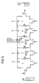
- the process parameters are explained in more detail in the description of FIG. 5.
- FIG. 3 The silicon substrate wafers 10, 11, 12, which are completely covered with the tantalum silicide or tungsten silicide layer (16), are subjected to a halogen-containing plasma in an anisotropic etching step and the tantalum silicide (or tungsten silicide) is removed from the horizontal surfaces of the arrangement. Only the side walls of the contact hole 13 remain covered with the tantalum silicide 16.
- FIG. 4 shows the arrangement after refilling the contact hole 13 by selective deposition of the tantalum silicide 17 from the gas phase.
- the process parameters are set so that tantalum silicide is only deposited on the silicon or tantalum silicide surfaces (see also European patent application 0 090 319).
- the continuous system is first described using the example of filling contact holes with tantalum silicide.
- the 150 mm structured silicon wafer (denoted by 10, 11, 12 in FIGS. 2 to 4, not shown in FIG. 5) is automatically introduced from the transport container 20 into the actual coating chamber 2 via a vacuum lock 1 with a folding valve 23 (23) , where it is first quickly heated to 650 ° C on a hot table 8.
- a gas mixture of silane, hydrogen, and tantalum pentachloride e.g. silane: 20 ml / min, hydrogen: 100 to 400 ml / min, tantalum pentachloride partial pressure: about 2 x 10- 1 mbar.
- the total pressure during the coating is preferably in the range from 150 to 200 ⁇ bar, with a deposition rate of approximately 20 to 70 nm / min of tantalum silicide.
- the substrate wafer coated with tantalum silicide over the entire surface is then transported from the chamber 2 via a further folding valve 23 into a second reaction chamber 3, where the anisotropic etching step is now carried out, for example consists of plasma etching in a boron trichloride / chlorine atmosphere at a total pressure of, for example, 30 ⁇ bar.
- the substrate temperature is a maximum of 650 ° C.
- Electrode with high-frequency generator are marked with 18 and 19.
- the silicon crystal wafer is transported via a further folding valve 23 into a fourth (4) or back into the second vacuum chamber (2), where the actual contact hole filling takes place by selective deposition of tantalum silicide.
- a gas mixture of silane, hydrogen, tantalum pentachloride and hydrogen chloride or dichlorosilane, hydrogen and tantalum pentachloride is used for this (dichlorosilane: 20 ml / min, hydrogen: 1000 ml / min, tantalum pentachloride partial pressure: approx. 200 Il bar).
- the coating temperature (heating table 8) for the selective deposition is also 650 ° C. under the selected conditions. Contact holes up to 1 ⁇ m deep can be filled at a rate of approx. 30 nm / min.
- the total pressure is, for example, 550 ⁇ bar.
- the silicon wafer is automatically transported out of the coating chamber 4 or 2 via a lock 5 or 1 and deposited in a transport container 21 or 20.
- the reference number 6 denotes gas inlets for ventilation gases, with 7 connections for a high vacuum pumping station and with 9 gas inlet systems for the respective reaction gases.
- a tungsten silicide layer is first deposited over the entire area in vacuum chamber 2 at, for example, 360 ° C. (table 8), tungsten hexafluoride being used as the tungsten compound (tungsten hexafluoride: 10 ml / min, silane: 1000 ml / min, inert gas for example helium: 200 ml / min, total pressure approx. 300 ⁇ bar, deposition rate approx. 30 nm / min; further details on the deposition can be found in an article by DL Brors et al. in "Semiconductor International", May 1984, pages 82 up to 85).
- the tungsten silicide in chamber 3 is then anisotropically etched in the plasma (18, 19), for example in sulfur hexafluoride at a total pressure of 330 ⁇ bar.
- tungsten hexafluoride 100 ml / min is used in chamber 4.
- hydrogen gas is additionally mixed in, so that tungsten is now formed by hydrogen reduction of the tungsten hexafluoride.
- 100 ml / min of tungsten hexafluoride with an additional 1000 ml / min of hydrogen are used again.
- the deposition rate is approx. 30 nm / min, the total pressure approx. 250 li bar.
- the selective molybdenum deposition is analogous to the tungsten deposition, with molybdenum pentafluoride being used as the starting substance.
- tungsten silicide, molybdenum silicide, niobium silicide or titanium silicide tungsten hexafluoride, molybdenum pentafluoride, niobium pentachloride or titanium tetrachloride together with dichlorosilane and hydrogen are reacted analogously to the selective tantalum silicide deposition.
Abstract
Description
Die Erfindung betrifft ein Verfahren zum selektiven Auffüllen von in Isolationsschichten geätzten Kontaktlöchern oder via holes (das sind relativ kleine Löcher, die zwischen den Leitbahnebenen hergestellt werden) mit metallisch leitenden Materialien, wie sie insbesondere zur Herstellung von höchstintegrierten Halbleiterschaltungen zur Ausbildung von elektrischen Leitbahnen auf strukturierten Halbleitersubstraten erforderlich sind, sowie eine Vorrichtung zur Durchführung des Verfahrens.The invention relates to a method for the selective filling of contact holes etched in insulation layers or via holes (these are relatively small holes that are produced between the interconnect levels) with metallically conductive materials, such as those used in particular for the production of highly integrated semiconductor circuits for the formation of electrical interconnects on structured ones Semiconductor substrates are required, and an apparatus for performing the method.
Bei der fortschreitenden Miniaturisierung von Halbleiterbauelementen treten bereits Strukturen im Bereich von 1 Ilm und darunter auf. Um die sehr kleinen aktiven Bereiche auf dem Halbleitersubstrat elektrisch ansteuern zu können, müssen diese mit metallischen Leitbahnen verbunden werden. Damit dieser Kontakt nur an definierten Stellen stattfindet, ist die Leitbahn durch eine Isolationsschicht, zum Beispiel aus Si02 bestehend, vom Halbleitersubstrat getrennt. Die Verbindung zu den aktiven Bereichen des Halbleitersubstrats findet über Kontaktlöcher statt, die in die Isolationsschicht eingeätzt werden.With the advancing miniaturization of semiconductor components, structures in the range of 1 Ilm and below are already appearing. In order to be able to electrically control the very small active areas on the semiconductor substrate, these must be connected to metallic interconnects. So that this contact only takes place at defined points, the interconnect is separated from the semiconductor substrate by an insulation layer, for example consisting of SiO 2 . The connection to the active areas of the semiconductor substrate takes place via contact holes which are etched into the insulation layer.
Analoge Verhältnisse herrschen auch bei höchstintegrierten Halbleiterschaltungen, bei denen zwei und mehr Leitbahnebenen für die elektrische Versorgung der sehr dicht gepackten aktiven Bereiche notwendig sind. Auch in diesem Fall muß ein elektrischer Kontakt durch sehr kleine Löcher (via holes) zwischen den verschiedenen Leitbahnebenen hergestellt werden.The situation is similar in the case of highly integrated semiconductor circuits in which two or more interconnect levels are necessary for the electrical supply of the very densely packed active areas. In this case, too, electrical contact must be made through very small holes (via holes) between the different interconnect levels.
Da aufgrund von schaltungstechnischen Überlegungen (zum Beispiel parasitäre Kapazitäten) die Isolationsschicht eine Mindestdicke von 0,7 bis 1,5 µm besitzen muß, treten bei den Kontaktlöchern bzw. via holes Tiefen/Durchmesserverhältnisse von größer/gleich 1 auf. Bei diesen sehr kleinen und tiefen Kontaktlöchern nimmt die Schichtdicke der Leitbahnen an den Flanken des Kontaktloches sehr stark ab (55 bis 80 % Abnahme), wenn das Leitbahnmaterial, zum Beispiel Aluminiumlegierungen : Aluminium-Silizium- (1 %), wie bisher üblich durch Kathodenzerstäubung (Sputtern) aufgebracht wird. Da die Leitbahnen mit extrem hohen Stromdichten belastet sind (zum Beispiel 1 x 10⁶ A/cm2), bewirkt eine jede Querschnittsverengung einen lokalen Temperaturanstieg, der an den Grenzflächen zwischen den verschiedenen Materialien im Kontakt einen unerwünschten Materialtransport (Diffusion, Reaktion) beschleunigt. Dies kann auch bis zum Durchbrennen einer Leitbahn führen.Since the insulation layer must have a minimum thickness of 0.7 to 1.5 µm due to circuitry considerations (for example parasitic capacitances), depth / diameter ratios of greater than / equal to 1 occur in the contact holes or via holes. In these very small and deep contact holes, the layer thickness of the interconnects on the flanks of the contact hole decreases very significantly (55 to 80% decrease) if the interconnect material, for example aluminum alloys: aluminum-silicon (1%), as previously customary by cathode sputtering (Sputtering) is applied. Since the interconnects are loaded with extremely high current densities (e.g. 1 x 10 6 A / cm 2 ), each cross-sectional narrowing causes a local temperature rise, which accelerates undesired material transport (diffusion, reaction) at the interfaces between the different materials in contact. This can also lead to the burnout of an interconnect.
Ein weiteres Problem besteht darin, wie aus der Figur 1 zu ersehen ist, daß sich in den Kontaktlöchern nach der Beschichtung zum Beispiel mit Aluminium-Silizium Hohlräume (15) ausbilden können. Wird nun daran anschließend eine Isolationsschicht, zum Beispiel als Unterlage für eine weitere Aluminium-Silizium-Leitbahnebene abgeschieden, so ist es praktisch nicht möglich, den im Kontaktloch befindlichen Hohlraum vollständig aufzufüllen. Da sich bei weiteren Fertigungsschritten in diesem Hohlraum zum Teil reaktive oder korrosive Medien ansammeln können, ist es für zuverlässige Bauelemente notwendig, ein Kontaktloch- bzw. via hole-Metallisierungsverfahren anzugeben, bei dem eine vollständige Auffüllung stattfindet.Another problem, as can be seen from FIG. 1, is that cavities (15) can form in the contact holes after coating, for example with aluminum-silicon. If an insulation layer is then subsequently deposited, for example as a base for a further aluminum-silicon interconnect level, it is practically not possible to completely fill up the cavity located in the contact hole. Since reactive or corrosive media can sometimes accumulate in this cavity during further production steps, it is necessary for reliable components to specify a contact hole or via hole metallization process in which complete filling takes place.
Aus dem Stand der Technik sind zum Auffüllen von Kontaktlöchern CVD (= chemical vapor deposition)-Verfahren bekannt, die sich durch eine sehr gute Kantenbedeckung auszeichnen. Es werden zwei verschiedene Methoden unterschieden:
- 1. Die ganzflächige Abscheidung der Metalliserungsschicht auf der Isolationsschicht einschließlich der Kontaktlöcher, unter Verwendung von Wolfram, wie sie aus einem Aufsatz von D. L. Brors et. al. aus Solid State Technol. April (1984), Seiten 313 bis 314, bekannt ist. Aufgrund der guten Kantenbedeckung des CVD-Verfahrens wächst die Schicht im Kontaktloch von allen Seiten etwa gleich schnell und füllt somit das Kontaktloch auf. Dieser Zustand ist bei einer Schichtdicke (gemessen auf horizontaler Struktur), die etwas mehr als der Hälfte des Kontaktlochdurchmessers entspricht, eingetreten. Ätzt man nun die Metallschicht wieder ganzflächig ab, so kann erreicht werden, daß das Metall von der Isolationsschicht vollständig entfernt ist, während das Kontaktloch noch mit Metall gefüllt bleibt.
- 2. Die selektive Abscheidung der Metallisierungsschicht in Kontaktlöchern unter Verwendung von Wolfram oder Tantalsilizid als Kontaktlochfüller, wie sie zum Beispiel für Wolfram aus einem Aufsatz von E. K. Broadbent et. al. in J. Electrochem. Soc., Solid State Sci. and Technol. (1984), Seiten 1427 bis 1433 oder für Tantalsilizid aus der Europäischen Patentanmeldung 0 090 319 bekannt ist. Bei den genannten CVD-Verfahren wird der Beschichtungsprozeß derart eingestellt, daß die chemische Reaktion, die die Beschichtung bewirkt, durch eine vorangehende Reaktion mit einem bestimmten Substratmaterial, zum Beispiel mit Silizium oder einer Siliziumlegierung, lokal ausgelöst werden kann. Es kann somit erreicht werden, daß das Kontaktloch voll ständig mit "Metall" aufgefüllt wird. So kann Wolfram bei Temperaturen um 360°C bis zu 1 µm Schichtdicke selektiv auf Silizium bzw. einer Siliziumlegierung abgeschieden werden. Aufgrund der die Selektivität auslösenden Reaktion (2 WFε+ 3 Si
- -7 3 SiF4+ 2 W) wird jedoch Silizium angeätzt (SiF4 besitzt einen hohen Dampfdruck), was zu Kurzschlüssen zwischen dem Dotierungsgebiet und dem Substrat führt.
- 1. The full-surface deposition of the metallization layer on the insulation layer including the contact holes, using tungsten, as described in an article by DL Brors et. al. from Solid State Technol. April (1984), pages 313 to 314. Due to the good edge coverage of the CVD process, the layer in the contact hole grows approximately equally quickly from all sides and thus fills the contact hole. This condition occurred at a layer thickness (measured on a horizontal structure) which corresponds to slightly more than half the contact hole diameter. If the entire metal layer is etched off again, it can be achieved that the metal is completely removed from the insulation layer, while the contact hole remains filled with metal.
- 2. The selective deposition of the metallization layer in contact holes using tungsten or tantalum silicide as contact hole filler, as described for example for tungsten from an article by EK Broadbent et. al. in J. Electrochem. Soc., Solid State Sci. and Technol. (1984), pages 1427 to 1433 or for tantalum silicide from European patent application 0 090 319 is known. In the case of the aforementioned CVD processes, the coating process is set such that the chemical reaction which effects the coating can be triggered locally by a preceding reaction with a specific substrate material, for example with silicon or a silicon alloy. It can thus be achieved that the contact hole is constantly filled with "metal". Tungsten can thus be selectively deposited on silicon or a silicon alloy at temperatures of around 360 ° C up to 1 µm layer thickness. Due to the selectivity-triggering reaction (2 WFε + 3 Si
- - 7 3 SiF 4 + 2 W), however, silicon is etched (SiF 4 has a high vapor pressure), which leads to short circuits between the doping region and the substrate.
Eine weitere Schwierigkeit bei diesem Verfahren besteht darin, daß zwischen dem selektiv aufwachsenden Metall und den aus Si02 bestehenden Seitenwänden des Kontaktloches nur eine schlechte Bindung besteht, so daß es hier lokal zu Haftungsproblemen und damit auch zu Hohlraumbildungen kommen kann.Another difficulty with this method is that there is only a poor bond between the selectively growing metal and the side walls of the contact hole consisting of SiO 2 , so that adhesion problems and thus also cavity formation can occur locally.
Das größte Problem bei einer selektiven Abscheidung besteht jedoch darin, daß die natürliche Oxidhaut in situ auf dem zu beschichtenden Silizium bzw. auf der Siliziumlegierung entfernt werden muß. Diese Maßnahme ist unbedingt erforderlich, um bei der Beschichtung eine ausreichende Selektivität gegenüber der Si02-Isolationsschicht zu erreichen.The biggest problem with selective deposition, however, is that the natural oxide skin has to be removed in situ on the silicon to be coated or on the silicon alloy. This measure is absolutely necessary in order to achieve sufficient selectivity with respect to the Si0 2 insulation layer in the coating.
Bei der selektiven Wolfram-Abscheidung bewirkt das Wolframhexafluorid bereits die Ätzung der ca. 3 nm dicken natürlichen Oxidhaut. Jedoch ist dieser Ätzschritt, der eine Nebenerscheingung des Beschichtungsprozesses darstellt, nur schwer zu steuern.In the case of selective tungsten deposition, the tungsten hexafluoride already causes the approx. 3 nm thick natural oxide skin to be etched. However, this etching step, which is a side effect of the coating process, is difficult to control.
Die selektive Tantalsilizid-Abscheidung mit Tantalpentachlorid als Metallausgangsverbindung bietet die Möglichkeit, vor der Beschichtung in situ einen eigenen Ätzschritt durchzuführen. Auch hier zeigt sich, daß ein definiertes Ätzen der natürlichen Oxidhaut (zum Beispiel mit Fluorwasserstoff) sehr schwierig ist. Vor allem gibt es keine Möglichkeit der Endpunktkontrolle, da die natür liche Oxidhaut sehr dünn ist und die Summe aller Kontaktlochflächen sehr klein ist im Vergleich zur Si02 -Isolationsschichtfiäche.The selective tantalum silicide deposition with tantalum pentachloride as the metal starting compound offers the possibility of carrying out a separate etching step in situ before the coating. Here, too, it can be seen that a defined etching of the natural oxide skin (for example with hydrogen fluoride) is very difficult. Above all, there is no possibility of endpoint control, since the natural oxide skin is very thin and the sum of all contact hole areas is very small compared to the Si0 2 insulation layer area.
Aufgabe der Erfindung ist es daher, ein Verfahren anzugeben, mit dem es möglich ist, in VLSI-Strukturen in sehr kleinen Kontaktlöchern und/oder via holes, die auf dem Silizium vorhandene Oxidhaut zu ätzen und daran anschließend die Kontaktlöcher und/oder via holes mit metallisch leitendem Material zu füllen, ohne daß Hohlräume an den Kontaktlochwänden entstehen können. Es ist weiterhin Aufgabe der Erfindung, eine Vorrichtung zur Durchführung dieses Verfahrens anzugeben.It is therefore the object of the invention to provide a method by which it is possible to etch the oxide skin present on the silicon in VLSI structures in very small contact holes and / or via holes and then also to etch the contact holes and / or via holes fill metallic conductive material without creating voids on the contact hole walls. It is also an object of the invention to provide an apparatus for performing this method.
Diese Aufgabe wird durch ein Verfahren gelöst, welches durch den Ablauf folgender Verfahrensschritte gekennzeichnet ist:
- a) ganzflächige Beschichtung der strukturierten, mit den Kontaktlöchern und/oder via holes versehenen Halbleitersubstrate mit einem Silizid eines hochschmelzenden Metalls durch eine chemische Abscheidung aus der Gasphase,
- b) anisotropes Ätzen der Substrate im Vakuum bis die Silizidschicht an den horizontalen Flächen des Substrats wieder entfernt ist und
- c) Auffüllen der Kontaktlöcher und/oder via holes mit dem metallisch leitenden Material durch selektive chemische Abscheidung aus der Gasphase.
- a) coating the entire surface of the structured semiconductor substrates provided with the contact holes and / or via holes with a silicide of a high-melting metal by chemical deposition from the gas phase,
- b) anisotropic etching of the substrates in vacuo until the silicide layer on the horizontal surfaces of the substrate is removed again and
- c) filling the contact holes and / or via holes with the metallic conductive material by selective chemical deposition from the gas phase.
Weitere Ausgestaltungen der Erfindung ergeben sich aus den Unteransprüchen.Further refinements of the invention result from the subclaims.
Durch dieses im wesentlichen dreistufige Verfahren ergeben sich folgende Vorteile:
- Nach der ganzflächigen Beschichtung mit einem Silizid eines hochschmelzenden Metalles nach Verfahrensschritt a), welche so lange durchgeführt wird, bis eine ca. 100 nm dicke Schicht an den Kontaktlochwänden entstanden ist, wird ein anisotroper Ätzprozeß durchgeführt. Dieser zeichnet sich dadurch aus, daß die Ätzrate für das vorher abgeschiedene Silizid an den horizontalen Flächen wesentlich höher ist als den vertikalen Flächen. Damit wird erreicht, daß das Silizid von den horizontalen Flächen vollständig entfernt werden kann, während an den vertikalen Kontaktlochwänden noch eine zusammenhängende Silizidschicht bestehen bleibt. Dieser Ätzschritt besitzt noch den weiteren Vorteil einer guten Endpunktkontrolle, da der horizontale Flächenanteil auf dem Substrat wesentlich größer ist als der vertikale. Ferner ist eine gewisse Über- ätzung des Silizids sogar notwendig, da hierbei auch die natürlich Oxidhaut beseitigt wird.
- After coating the entire surface with a silicide of a high-melting metal according to process step a), which is carried out until an approximately 100 nm thick layer has formed on the contact hole walls, an anisotropic etching process is carried out. This is characterized by the fact that the etching rate for the previously deposited silicide is much higher on the horizontal surfaces than on the vertical surfaces. The result is that the silicide can be completely removed from the horizontal surfaces, while a continuous silicide layer remains on the vertical contact hole walls. This etching step has the further advantage of good end point control, since the horizontal surface area on the substrate is considerably larger than the vertical one. Furthermore, a certain over-etching of the silicide is even necessary, since this also removes the natural oxide skin.
Wesentlich ist nun, daß die so behandelten Scheiben nach dem Ätzen nicht an Luft gelangen, sondern ohne Unterbrechung des Vakuums selektiv mit zum Beispiel Molybdän, Molybdänsilizid, Wolfram, Wolframsilizid, Tantalsilizid, Titansilizid oder Niobsilizid beschichtet werden. Da sich nun keine Oxidhaut mehr auf dem Kontaktlochboden befindet, bildet sich sehr schnell eine zusammenhängende, dichte Metall- bzw. Silizidschicht, die auch gut an den mit Silizid vorbeschichteten Kontaktlochwänden haftet.It is essential that the wafers treated in this way do not get into the air after the etching, but instead are selectively coated with, for example, molybdenum, molybdenum silicide, tungsten, tungsten silicide, tantalum silicide, titanium silicide or niobium silicide without interrupting the vacuum. Since there is no longer an oxide skin on the contact hole bottom, a coherent, dense metal or silicide layer forms very quickly, which also adheres well to the contact hole walls precoated with silicide.
Im folgenden wird anhand von zwei Ausführungsbeispielen und der Figuren 1 bis 5 die Erfindung noch näher erläutert. Dabei zeigen:
- die Figur 1 schematisch im Schnittbild eine Kontaktlochauffüllung durch Sputtern, wie sie aus dem Stand der Technik bekannt ist,
- die
Figuren 2bis 4 im Schnittbild die erfindungswesent lichen Verfahrensschritte zur Kontaktloch- bzw. via hole-Auffüllung und - die
Figur 5 schematisch eine aus fünf Vakuumkammern bestehende Einscheiben-Durchlaufanlage, wie sie mit Vorteil für das erfindungsgemäße Verfahren verwendet wird.
- 1 schematically shows a contact hole filling by sputtering, as is known from the prior art,
- Figures 2 to 4 in sectional view, the process steps essential to the invention for contact hole or via hole filling and
- 5 shows schematically a single-disc continuous system consisting of five vacuum chambers, as is advantageously used for the method according to the invention.
Figur 1: Mit dem Bezugszeichen 10 ist die auf dem Siliziumsubstrat 11 mit der dotierten Zone 12 befindliche SiOz-Schicht bezeichnet, welche das ca. 1 J.Lm tiefe und 1 J.Lm breite Kontaktloch 13 enthält. Das Kontaktloch 13 wurde mit einer aus einer Aluminium-Silizium-Legierung bestehenden, elektrisch leitenden Materialschicht 14 durch Sputtern aufgefüllt. Mit 15 ist der im Kontaktloch 13 entstandene Hohlraum (Kaverne) bezeichnet, der durch das Verfahren nach der Lehre der Erfindung sicher vermieden werden kann.Figure 1: The
Die Figur 2 zeigt den ersten Schritt des erfindungsgemäßen Verfahrens am Beispiel einer ganzflächigen LPCVD-(= low pressure chemical vapor deposition)-Abscheidung von Tantalsilizid 16 für ein, in eine Si02-Schicht 10 geätztes Kontaktloch 13 (oder von Wolframsilizid für ein via hole) auf ein mit einer dotierten Zone 12 versehenes Halbleitersubstrat 11. Die Abscheidung wird solange fortgesetzt bis an den Kontaktlochwänden ca. 100 nm Silizid abgeschieden ist. Die Verfahrensparameter werden bei der Beschreibung der Figur 5 näher erläutert.FIG. 2 shows the first step of the method according to the invention using the example of a full-surface LPCVD (= low pressure chemical vapor deposition) deposition of
Figur 3: Die mit der Tantalsilizid- oder Wolframsilizid-Schicht (16) ganzflächig bedeckten Silizium-Substratscheiben 10, 11, 12 werden in einem anisotropen Ätzschritt einem halogenhaltigen Plasma unterworfen und das Tantalsilizid (oder Wolframsilizid) an den horizontalen Flächen der Anordnung entfernt. Bedeckt mit dem Tantalsilizid 16 bleiben nur die Seitenwände des Kontaktlochs 13.FIG. 3: The
Figur 4 zeigt die Anordnung nach dem Wiederauffüllen des Kontaktloches 13 durch selektive Abscheidung vom Tantalsilizid 17 aus der Gasphase. Dabei werden die Prozeßparameter so eingestellt, daß sich Tantalsilizid nur auf den Silizium- bzw. Tantalsilizid-Flächen abscheidet (siehe auch europäische Patentanmeldung 0 090 319).FIG. 4 shows the arrangement after refilling the
Die Durchlaufanlage wird zunächst am Beispiel des Auffüllens von Kontaktlöchern mit Tantalsilizid beschrieben.The continuous system is first described using the example of filling contact holes with tantalum silicide.
Über eine Vakuumschleuse 1 mit einem Klappventil 23 wird die 150 mm große strukturierte Siliziumscheibe (in den Figuren 2 bis 4 mit 10, 11, 12 bezeichnet, in Figur 5 nicht dargestellt) aus dem Transportbehälter 20 automatisch in die eigentliche Beschichtungskammer 2 eingeschleust (23), wo sie zunächst rasch auf einem Heiztisch 8 auf 650°C erhitzt wird. Zur ganzflächigen Tantalsilizid-Abscheidung wird eine Gasmischung aus Silan, Wasserstoff und Tantalpentachlorid verwendet (zum Beispiel Silan: 20 ml/min, Wasserstoff: 100 bis 400 ml/min, Tantalpentachlorid-Partialdruck: ca. 2 x 10⁻¹ mbar). Der Gesamtdruck während der Beschichtung liegt vorzugsweise im Bereich von 150 bis 200 µbar, wobei sich eine Abscheiderate von ca. 20 bis 70 nm/min Tantalsilizid ergibt.The 150 mm structured silicon wafer (denoted by 10, 11, 12 in FIGS. 2 to 4, not shown in FIG. 5) is automatically introduced from the
Nach zum Beispiel 1,5 Minuten wird (entsprechend ca. 100 nm Schichtdicke) nun die mit Tantalsilizid ganzflächig beschichtete Substratscheibe aus der Kammer 2 über ein weiteres Klappventil 23 in eine zweite Reaktionskammer 3 transportiert, wo nun der anisotrope Ätzschritt durchgeführt wird, der zum Beispiel aus Plasmaätzen in einer Bortrichlorid/Chlor-Atmosphäre bei einem Gesamtdruck von zum Beispiel 30 µbar besteht. Die Substrattemperatur be trägt maximal 650°C. Elektrode mit Hochfrequenzgenerator sind mit 18 und 19 gekennzeichnet.After, for example, 1.5 minutes (corresponding to a layer thickness of approximately 100 nm), the substrate wafer coated with tantalum silicide over the entire surface is then transported from the
Nach Beendigung des Ätzschrittes in der Kammer 3 wird die Siliziumkristallscheibe über ein weiteres Klappventil 23 in eine vierte (4) oder wieder in die zweite Vakuumkammer (2) transportiert, wo nun die eigentliche Kontaktlochauffüllung durch selektive Abscheidung von Tantalsilizid stattfindet. Hierzu wird ein Gasgemisch aus Silan, Wasserstoff, Tantalpentachlorid und Chlorwasserstoff oder Dichlorsilan, Wasserstoff und Tantalpentachlorid verwendet (Dichlorsilan: 20 ml/min, Wasserstoff: 1000 ml/min, Tantalpentachlorid-Partialdruck: ca. 200 Ilbar). Die Beschichtungstemperatur (Heiztisch 8) für die selektive Abscheidung beträgt unter den gewählten Bedingungen ebenfalls 650°C. Es lassen sich dabei bis zu 1 µm tiefe Kontaktlöcher mit einer Rate von ca. 30 nm/min auffüllen. Der Gesamtdruck liegt zum Beispiel bei 550 µbar.After the etching step in
Nach Abschluß der selektiven Beschichtung wird die Siliziumscheibe automatisch über eine Schleuse 5 bzw. 1 aus der Beschichtungskammer 4 bzw. 2 transportiert und in einem Transportbehälter 21 bzw. 20 deponiert.After completion of the selective coating, the silicon wafer is automatically transported out of the
Es ist offensichtlich, daß eine CVD-Anlage mit drei Vakuumkammern (2, 3, 4) einen höheren Durchsatz bietet als eine aus zwei Kammern, da während der selektiven Beschichtung in der Kammer 4 bereits eine weitere Siliziumsubstratscheibe in der Kammer 2 ganzflächig mit Tantalsilizid belegt werden kann.It is obvious that a CVD system with three vacuum chambers (2, 3, 4) offers a higher throughput than one from two chambers, since during the selective coating in
Mit dem Bezugszeichen 6 sind Gaseinlässe für Belüftungsgase, mit 7 Anschlüsse für einen Hochvakuumpumpstand und mit 9 Gaseinlaßsysteme für die jeweiligen Reaktionsgase bezeichnet.The
Auffüllen von via holes mit Wolfram.Filling via holes with tungsten.
Analog zur Tantalsilizidabscheidung wird zunächst in der Vakuumkammer 2 ganzflächig eine Wolframsilizid-Schicht bei zum Beispiel 360°C (Tisch 8) abgeschieden, wobei Wolframhexafluorid als Wolfram-Verbindung verwendet wird (Wolframhexafluorid: 10 ml/min, Silan: 1000 ml/min, Inertgas zum Beispiel Helium: 200 ml/min, Gesamtdruck ca. 300 µbar, Abscheiderate ca. 30 nm/min; nähere Einzelheiten über die Abscheidung sind aus einem Aufsatz von D. L. Brors et. al. in "Semiconductor International", Mai 1984, Seiten 82 bis 85, zu entnehmen).Analogous to tantalum silicide deposition, a tungsten silicide layer is first deposited over the entire area in
Anschließend wird das Wolframsilizid in der Kammer 3 anisotrop im Plasma (18, 19) geätzt, zum Beispiel in Schwefelhexafluorid bei einem Gesamtdruck von 330 µbar.The tungsten silicide in
Für die selektive Wolfram-Abscheidung wird in Kammer 4 Wolframhexafluorid (100 ml/min) verwendet. Nachdem sich eine geschlossene Wolframschicht durch Reduktion des Wolframhexafluorids durch Silizium gebildet hat, wird Wasserstoffgas zusätzlich beigemischt, so daß jetzt Wolfram durch Wasserstoffreduktion des Wolframhexafluorid gebildet wird. Dabei werden wieder ca. 100 ml/min Wolframhexafluorid mit zusätzlich 1000 ml/min Wasserstoff verwendet. Die Abscheiderate beträgt ca. 30 nm/min, der Gesamtdruck ca. 250 libar.For selective tungsten deposition, tungsten hexafluoride (100 ml / min) is used in
Aufgrund der wesentlich höheren Keimbildungsgeschwindigkeit von Wolfram auf Wolfram im Vergleich zu Wolfram auf Si02 kann eine selektive Wolfram-Abscheidung bis zu 1 µm Dicke erreicht werden, ohne daß sich auch auf dem Oxid Wolfram-Keime bilden.Due to the significantly higher nucleation rate of tungsten on tungsten compared to tungsten on Si0 2 , a selective tungsten deposition down to 1 µm in thickness can be achieved without tungsten seeds also forming on the oxide.
Die selektive Molybdän-Abscheidung verläuft analog zur Wolfram-Abscheidung, wobei Molybdänpentafluorid als Aus gangssubstanz verwendet wird.The selective molybdenum deposition is analogous to the tungsten deposition, with molybdenum pentafluoride being used as the starting substance.
Für die selektive Abscheidung von Wolframsilizid, Molybdänsilizid, Niobsilizid oder Titansilizid werden Wolframhexafluorid, Molybdänpentafluorid, Niobpentachlorid oder Titantetrachlorid zusammen mit Dichlorsilan und Wasserstoff analog zur selektiven Tantalsilizid-Abscheidung zur Reaktion gebracht.For the selective deposition of tungsten silicide, molybdenum silicide, niobium silicide or titanium silicide, tungsten hexafluoride, molybdenum pentafluoride, niobium pentachloride or titanium tetrachloride together with dichlorosilane and hydrogen are reacted analogously to the selective tantalum silicide deposition.
Claims (12)
Priority Applications (1)
| Application Number | Priority Date | Filing Date | Title |
|---|---|---|---|
| AT86110076T ATE46791T1 (en) | 1985-07-29 | 1986-07-22 | METHOD FOR SELECTIVE FILLING OF CONTACT HOLES ETCHED IN INSULATING LAYERS WITH METALLIC CONDUCTIVE MATERIALS IN THE MANUFACTURE OF HIGHLY INTEGRATED SEMICONDUCTOR CIRCUITS AND A DEVICE FOR CARRYING OUT THE METHOD. |
Applications Claiming Priority (2)
| Application Number | Priority Date | Filing Date | Title |
|---|---|---|---|
| DE3527132 | 1985-07-29 | ||
| DE3527132 | 1985-07-29 |
Publications (2)
| Publication Number | Publication Date |
|---|---|
| EP0211318A1 EP0211318A1 (en) | 1987-02-25 |
| EP0211318B1 true EP0211318B1 (en) | 1989-09-27 |
Family
ID=6277076
Family Applications (1)
| Application Number | Title | Priority Date | Filing Date |
|---|---|---|---|
| EP86110076A Expired EP0211318B1 (en) | 1985-07-29 | 1986-07-22 | Process for selectively filling contact holes made by etching in insulating layers with electrically conductive materials for the manufacture of high-density integrated semiconductor circuits, and apparatus used for this process |
Country Status (3)
| Country | Link |
|---|---|
| EP (1) | EP0211318B1 (en) |
| AT (1) | ATE46791T1 (en) |
| DE (1) | DE3665961D1 (en) |
Families Citing this family (11)
| Publication number | Priority date | Publication date | Assignee | Title |
|---|---|---|---|---|
| US5084413A (en) * | 1986-04-15 | 1992-01-28 | Matsushita Electric Industrial Co., Ltd. | Method for filling contact hole |
| US4924295A (en) * | 1986-11-28 | 1990-05-08 | Siemens Aktiengesellschaft | Integrated semi-conductor circuit comprising at least two metallization levels composed of aluminum or aluminum compounds and a method for the manufacture of same |
| WO1988004831A1 (en) * | 1986-12-19 | 1988-06-30 | Hughes Aircraft Company | Conductive plug for contacts and vias on integrated circuits |
| FR2624304B1 (en) * | 1987-12-04 | 1990-05-04 | Philips Nv | METHOD FOR ESTABLISHING AN ELECTRICAL INTERCONNECTION STRUCTURE ON A SILICON SEMICONDUCTOR DEVICE |
| NL8800221A (en) * | 1988-01-29 | 1989-08-16 | Philips Nv | METHOD FOR MANUFACTURING A SEMICONDUCTOR DEVICE |
| EP0348119B1 (en) * | 1988-06-23 | 1997-08-13 | Kabushiki Kaisha Toshiba | Method of processing metal connectors on semi-conductor devices |
| KR930004295B1 (en) * | 1988-12-24 | 1993-05-22 | 삼성전자 주식회사 | Connecting method of low resistance |
| JPH02257640A (en) * | 1989-03-30 | 1990-10-18 | Oki Electric Ind Co Ltd | Manufacture of semiconductor element |
| KR0171069B1 (en) * | 1994-10-27 | 1999-03-30 | 문정환 | Method of forming metal contact of semiconductor device |
| US5783485A (en) * | 1996-07-19 | 1998-07-21 | Motorola, Inc. | Process for fabricating a metallized interconnect |
| US6077768A (en) * | 1996-07-19 | 2000-06-20 | Motorola, Inc. | Process for fabricating a multilevel interconnect |
Family Cites Families (2)
| Publication number | Priority date | Publication date | Assignee | Title |
|---|---|---|---|---|
| US4361599A (en) * | 1981-03-23 | 1982-11-30 | National Semiconductor Corporation | Method of forming plasma etched semiconductor contacts |
| DE3211752C2 (en) | 1982-03-30 | 1985-09-26 | Siemens AG, 1000 Berlin und 8000 München | Process for the selective deposition of layer structures consisting of silicides of refractory metals on substrates consisting essentially of silicon and their use |
-
1986
- 1986-07-22 AT AT86110076T patent/ATE46791T1/en active
- 1986-07-22 EP EP86110076A patent/EP0211318B1/en not_active Expired
- 1986-07-22 DE DE8686110076T patent/DE3665961D1/en not_active Expired
Also Published As
| Publication number | Publication date |
|---|---|
| EP0211318A1 (en) | 1987-02-25 |
| ATE46791T1 (en) | 1989-10-15 |
| DE3665961D1 (en) | 1989-11-02 |
Similar Documents
| Publication | Publication Date | Title |
|---|---|---|
| DE10230088B4 (en) | Method for producing a semiconductor device | |
| EP0090318B1 (en) | Process for manufacturing integrated circuits comprising mos field-effect transistors using silicon gate technology having silicide layers on diffusion regions as low-ohmic conductors | |
| DE3231987C2 (en) | A method for producing a cobalt silicide layer in a semiconductor device | |
| DE2951734C2 (en) | ||
| DE4430120B4 (en) | Process for the production of a dielectric | |
| DE4237587C2 (en) | Chemical vapor deposition process to create a predominantly TiSi¶x¶ containing, electrically conductive layer | |
| EP0094528A2 (en) | Process for producing double-layer structures consisting of metal silicide and polysilicium on substrates containing integrated circuits by reactive ion etching | |
| DE19627017A1 (en) | Process for the selective deposition of a metal film | |
| EP0211318B1 (en) | Process for selectively filling contact holes made by etching in insulating layers with electrically conductive materials for the manufacture of high-density integrated semiconductor circuits, and apparatus used for this process | |
| DE19620022A1 (en) | Method for producing a diffusion barrier metal layer in a semiconductor device | |
| EP0269095A2 (en) | Integrated semiconductor circuit with at least two planes made of aluminium or aluminium compound and method of manufacturing the same | |
| EP0090319A1 (en) | Process for the selective deposition of layered structures consisting of silicides of high melting metals on substrates essentially consisting of silicon, and their use | |
| DE4214091C2 (en) | ||
| DE2845460A1 (en) | METHOD OF MANUFACTURING A SEMICONDUCTOR DEVICE | |
| DE2430692A1 (en) | PROCESS FOR PRODUCING CONNECTING HOLES IN INSULATING LAYERS | |
| DE60114383T2 (en) | METHOD AND DEVICE FOR PLASMA COATING | |
| DE19844102A1 (en) | Manufacturing process for a semiconductor structure | |
| DE102004030612B3 (en) | Semiconductor substrate and method for its production | |
| DE10154346A1 (en) | Filling of substrate wells with SiO ¶¶2¶¶ by HDP vapor deposition with the participation of H¶¶2¶¶O¶¶2¶¶ or H¶¶2¶¶O as reaction gas | |
| DE69931656T2 (en) | METHOD FOR PRODUCING A SiON / SiO 2 DIELECTRIC INTERMEDIATE LAYER WITH POST-TREATMENT OF THE CVD SILICON OXYNITRIDE LAYER | |
| DE69724965T2 (en) | METHOD FOR SIMPLIFYING THE PRODUCTION OF A DIELECTRIC INTERLAYER STACK | |
| DE102004062472A1 (en) | Fabrication of metal interconnection line in semiconductor device by nitriding the metal layer to form a barrier metal layer, and forming metal interconnection line on barrier metal layer by burying the contact openings | |
| EP0855088B1 (en) | Process for producing trench insulation in a substrate | |
| DE10085212B4 (en) | Dielectric layer, integrated circuit and method of making the same | |
| DE3742912A1 (en) | METHOD FOR PRODUCING SEMICONDUCTOR CIRCUITS |
Legal Events
| Date | Code | Title | Description |
|---|---|---|---|
| PUAI | Public reference made under article 153(3) epc to a published international application that has entered the european phase |
Free format text: ORIGINAL CODE: 0009012 |
|
| AK | Designated contracting states |
Kind code of ref document: A1 Designated state(s): AT CH DE FR GB IT LI NL |
|
| 17P | Request for examination filed |
Effective date: 19870807 |
|
| 17Q | First examination report despatched |
Effective date: 19890124 |
|
| GRAA | (expected) grant |
Free format text: ORIGINAL CODE: 0009210 |
|
| AK | Designated contracting states |
Kind code of ref document: B1 Designated state(s): AT CH DE FR GB IT LI NL |
|
| REF | Corresponds to: |
Ref document number: 46791 Country of ref document: AT Date of ref document: 19891015 Kind code of ref document: T |
|
| REF | Corresponds to: |
Ref document number: 3665961 Country of ref document: DE Date of ref document: 19891102 |
|
| ET | Fr: translation filed | ||
| ITF | It: translation for a ep patent filed |
Owner name: STUDIO JAUMANN |
|
| GBT | Gb: translation of ep patent filed (gb section 77(6)(a)/1977) | ||
| PLBE | No opposition filed within time limit |
Free format text: ORIGINAL CODE: 0009261 |
|
| STAA | Information on the status of an ep patent application or granted ep patent |
Free format text: STATUS: NO OPPOSITION FILED WITHIN TIME LIMIT |
|
| 26N | No opposition filed | ||
| PG25 | Lapsed in a contracting state [announced via postgrant information from national office to epo] |
Ref country code: NL Effective date: 19910201 |
|
| NLV4 | Nl: lapsed or anulled due to non-payment of the annual fee | ||
| ITTA | It: last paid annual fee | ||
| PGFP | Annual fee paid to national office [announced via postgrant information from national office to epo] |
Ref country code: GB Payment date: 19930618 Year of fee payment: 8 |
|
| PGFP | Annual fee paid to national office [announced via postgrant information from national office to epo] |
Ref country code: AT Payment date: 19930623 Year of fee payment: 8 |
|
| PGFP | Annual fee paid to national office [announced via postgrant information from national office to epo] |
Ref country code: FR Payment date: 19930716 Year of fee payment: 8 |
|
| PGFP | Annual fee paid to national office [announced via postgrant information from national office to epo] |
Ref country code: DE Payment date: 19930915 Year of fee payment: 8 |
|
| PGFP | Annual fee paid to national office [announced via postgrant information from national office to epo] |
Ref country code: CH Payment date: 19931019 Year of fee payment: 8 |
|
| PG25 | Lapsed in a contracting state [announced via postgrant information from national office to epo] |
Ref country code: GB Effective date: 19940722 Ref country code: AT Effective date: 19940722 |
|
| PG25 | Lapsed in a contracting state [announced via postgrant information from national office to epo] |
Ref country code: LI Effective date: 19940731 Ref country code: CH Effective date: 19940731 |
|
| GBPC | Gb: european patent ceased through non-payment of renewal fee |
Effective date: 19940722 |
|
| PG25 | Lapsed in a contracting state [announced via postgrant information from national office to epo] |
Ref country code: FR Effective date: 19950331 |
|
| REG | Reference to a national code |
Ref country code: CH Ref legal event code: PL |
|
| PG25 | Lapsed in a contracting state [announced via postgrant information from national office to epo] |
Ref country code: DE Effective date: 19950401 |
|
| REG | Reference to a national code |
Ref country code: FR Ref legal event code: ST |
|
| PG25 | Lapsed in a contracting state [announced via postgrant information from national office to epo] |
Ref country code: IT Free format text: LAPSE BECAUSE OF NON-PAYMENT OF DUE FEES Effective date: 20050722 |