EP0053711A2 - Method of making layer structures from silicides or silicides-polysilicon by reactive sputter etching - Google Patents
Method of making layer structures from silicides or silicides-polysilicon by reactive sputter etching Download PDFInfo
- Publication number
- EP0053711A2 EP0053711A2 EP81109137A EP81109137A EP0053711A2 EP 0053711 A2 EP0053711 A2 EP 0053711A2 EP 81109137 A EP81109137 A EP 81109137A EP 81109137 A EP81109137 A EP 81109137A EP 0053711 A2 EP0053711 A2 EP 0053711A2
- Authority
- EP
- European Patent Office
- Prior art keywords
- etching
- silicides
- polysilicon
- power
- reactive sputter
- Prior art date
- Legal status (The legal status is an assumption and is not a legal conclusion. Google has not performed a legal analysis and makes no representation as to the accuracy of the status listed.)
- Granted
Links
Images
Classifications
-
- H—ELECTRICITY
- H01—ELECTRIC ELEMENTS
- H01L—SEMICONDUCTOR DEVICES NOT COVERED BY CLASS H10
- H01L21/00—Processes or apparatus adapted for the manufacture or treatment of semiconductor or solid state devices or of parts thereof
- H01L21/02—Manufacture or treatment of semiconductor devices or of parts thereof
- H01L21/04—Manufacture or treatment of semiconductor devices or of parts thereof the devices having at least one potential-jump barrier or surface barrier, e.g. PN junction, depletion layer or carrier concentration layer
- H01L21/18—Manufacture or treatment of semiconductor devices or of parts thereof the devices having at least one potential-jump barrier or surface barrier, e.g. PN junction, depletion layer or carrier concentration layer the devices having semiconductor bodies comprising elements of Group IV of the Periodic System or AIIIBV compounds with or without impurities, e.g. doping materials
- H01L21/30—Treatment of semiconductor bodies using processes or apparatus not provided for in groups H01L21/20 - H01L21/26
- H01L21/31—Treatment of semiconductor bodies using processes or apparatus not provided for in groups H01L21/20 - H01L21/26 to form insulating layers thereon, e.g. for masking or by using photolithographic techniques; After treatment of these layers; Selection of materials for these layers
- H01L21/3205—Deposition of non-insulating-, e.g. conductive- or resistive-, layers on insulating layers; After-treatment of these layers
- H01L21/321—After treatment
- H01L21/3213—Physical or chemical etching of the layers, e.g. to produce a patterned layer from a pre-deposited extensive layer
- H01L21/32133—Physical or chemical etching of the layers, e.g. to produce a patterned layer from a pre-deposited extensive layer by chemical means only
- H01L21/32135—Physical or chemical etching of the layers, e.g. to produce a patterned layer from a pre-deposited extensive layer by chemical means only by vapour etching only
- H01L21/32136—Physical or chemical etching of the layers, e.g. to produce a patterned layer from a pre-deposited extensive layer by chemical means only by vapour etching only using plasmas
- H01L21/32137—Physical or chemical etching of the layers, e.g. to produce a patterned layer from a pre-deposited extensive layer by chemical means only by vapour etching only using plasmas of silicon-containing layers
Definitions
- the present patent application relates to a method for producing structures of layers consisting of silicides or double layers consisting of silicide-polysilicon on substrates containing integrated semiconductor circuits by reactive sputter etching (ion etching) with sulfur hexafluoride (SF 6 ) as an etching gas using a photoresist etching mask.
- reactive sputter etching ion etching
- sulfur hexafluoride SF 6
- anisotropic etching processes are used in the etching technology in order to ensure a dimensionally accurate structure transfer.
- Such an anisotropic etching process is described in Chemical Abstracts, Vol. 85, 1976, p. 562, left column, known.
- CF 4 Freon
- a further selectivity of polysilicon to Si0 2 and Si 3 N 4 is obtained if a gas mixture of sulfur hexafluoride (SF 6 ), chlorine and inert gas is used in the etching of silicon (see European patent application 0015403).
- SF 6 sulfur hexafluoride
- chlorine and inert gas is used in the etching of silicon.
- the etching process is carried out in two steps, first with an RF power of greater than 0.3 W / cm 2 with a high etching rate and then with an RF power of less than 0.2 W / cm 2 is etched with a lower etching rate.
- the first process step achieves strict anisotropy
- the second process step good selectivity to SiO 2 .
- the silicon substrates are folded over with metal rings, preferably made of aluminum, in order to make the etching attack more uniform.
- metal rings preferably made of aluminum
- the height of the rings must be chosen correctly. In the exemplary embodiment, 4 mm are optimal. To avoid contamination of the discs, it is advantageous to use high-purity aluminum for the rings.
- the method according to the invention is particularly suitable for the production of structures consisting of tungsten, molybdenum and tantalum silicide.
- structures consisting of tungsten, molybdenum and tantalum silicide With hexafluoride (SF 6 ) silicides of any metal content can be etched. The etching rate decreases with increasing metal content.
- SF 6 hexafluoride
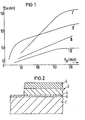
- polysilicon (curve II) already has a high etching rate at low RF powers; it is about three times as high as that of molybdenum silicide (curve III).
- the selectivity polysilicon (curve II) to Si0 2 (curve IV) is greater than 10: 1 in the second stage.
- Photoresist AZ 1450 I from Shipley
- the paint removal is in the range of the thickness of the etched double layer (approx. 500 nm).
- Figure 2 shows the example of a double layer 3 of 300 nm thick doped polysilicon 4 and an overlying 200 nm thick molybdenum silicide layer 5 with a molybdenum content of 35% that a strictly anisotropic etching process has taken place.
- the selectivity of the polysilicon layer 4 with respect to the underlying SiO 2 layer 6 is very high.
- Reference number 7 denotes the semiconductor substrate made of silicon. The paint mask has already been removed.
- the etching time for the double layer 3 consisting of polysilicon 4 and molybdenum silicide 5 is approximately 12 minutes in the method according to the invention; in known methods (e.g. etching in CF 4 plasma), the etching time is more than twice as long.
Abstract
Die Erfindung betrifft ein Verfahren zum Herstellen von Strukturen von aus Metallsiliziden oder aus Metallsilizid-Polysilizium bestehenden Doppelschichten (3) durch reaktives Sputterätzen mit Schwefelhexafluord (SF6) als Ätzgas. Dabei erfolgt der Ätzprozeß in zwei Schritten, wobei zunächst mit einer HF-Leistung von größer als 0,3 W/cm² und anschließend mit einer HF-Leistung von weniger als 0,2 W/cm² geätzt wird. Das Verfahren ist streng anisotrop auch bei Verwendung von Fotolack als Ätzmaske und wird angewandt bei der Herstellung hochintegrierter Halbleiterschaltungen in MOS-Technologie mit Metallsilizidschichten zur Verminderung des ohm'schen Widerstandes von Polysilizium.The invention relates to a method for producing structures of double layers (3) consisting of metal silicides or of metal silicide polysilicon by reactive sputter etching with sulfur hexafluoride (SF6) as the etching gas. The etching process takes place in two steps, first with an RF power of greater than 0.3 W / cm² and then with an RF power of less than 0.2 W / cm². The method is strictly anisotropic even when using photoresist as an etching mask and is used in the production of highly integrated semiconductor circuits in MOS technology with metal silicide layers to reduce the ohmic resistance of polysilicon.
Description
Die vorliegende Patentanmeldung betrifft ein Verfahren zum Herstellen von Strukturen von aus Siliziden bestehenden Schichten oder aus Silizid-Polysilizium bestehenden Doppelschichten auf integrierte Halbleiterschaltungen enthaltenden Substraten durch reaktives Sputterätzen (Ionenätzen) mit Schwefelhexafluorid (SF6) als'Ätzgas unter Verwendung einer Fotolackätzmaske.The present patent application relates to a method for producing structures of layers consisting of silicides or double layers consisting of silicide-polysilicon on substrates containing integrated semiconductor circuits by reactive sputter etching (ion etching) with sulfur hexafluoride (SF 6 ) as an etching gas using a photoresist etching mask.
Zur Herstellung hochintegrierter MOS-Schaltungen werden in der Ätztechnik anisotrope Ätzverfahren eingesetzt, um eine maßhaltige Strukturübertragung zu gewährleisten. Ein solches anisotropes Ätzverfahren ist aus dem Chemical Abstracts, Vol. 85, 1976, p. 562, linke Spalte, bekannt. Dabei werden Strukturen in polykristallinen Siliziumschichten in der Größenordnung von 10 /um durch reaktives Sputterätzen mit einer Mischung aus gasförmigen Sauerstoff und Tetrafluorkohlenstoff (CF4 = Freon) untersucht, wobei als Ätzmasken Filme-aus fotoempfindlichen Lacken verwendet werden. Das Ätzprofil der in den polykristallinen Siliziumschichten erzeugten Strukturen ist dabei weitgehend abhängig von der Dicke der Siliziumschicht sowie von der eingespeisten Hochfrequenzleistung.To produce highly integrated MOS circuits, anisotropic etching processes are used in the etching technology in order to ensure a dimensionally accurate structure transfer. Such an anisotropic etching process is described in Chemical Abstracts, Vol. 85, 1976, p. 562, left column, known. In this case, structures are to examined in polycrystalline silicon layers in the order of 10 / by reactive sputter etching with a mixture of gaseous oxygen and carbon tetrafluoride (CF 4 = Freon), which are used photosensitive coatings as etching masks of Movies-. The etching profile of the structures produced in the polycrystalline silicon layers is largely dependent on the thickness of the silicon layer and on the high-frequency power fed in.
Um den ohmrschen Widerstand von Polysiliziumbahnen bei der Herstellung von integrierten Schaltungen in der MOS-Technologie zu vermindern, werden die Polysiliziumbahnen durch Metallsilizide ersetzt oder auf die Polysiliziumbahnen eine zusätzliche Metallsilizidschicht (= "Polyzid"-Schicht) aufgebracht. Um hier eine Strukturerzeugung von Strukturen im Bereich von 1 /um durchzuführen, müssen anisotrope Ätzverfahren angewandt werden. Ein anisotropes Ätzverfahren für ein Silizid, bei dem CF4 als Ätzgas verwendet wird, ist aus den Transactions on Electron Devices, Vol. ED-26, No. 4, April 1979, aus einem Aufsatz von Crowder und Zirinsky auf den Seiten 369 bis 371 zu entnehmen. Das hier beschriebene Verfahren. ist streng anisotrop; Fotolack kann aber wegen der schlechten Selektivität zum Silizid als Ätzmaske nicht verwendet werden. Andere Masken, z. B. aus Aluminium, sind möglich, komplizieren aber den Prozeßablauf. Ein weiterer Nachteil ist, daß die Selektivität von Polysilizium zu SiO2 nur etwa 2:1 beträgt.In order to reduce the resistance of polysilicon ohm r rule webs in the manufacture of integrated circuits in MOS technology, the polysilicon tracks are replaced by metal silicides or poly silicon sheets an additional metal silicide layer (= "polycide" layer) applied. In order to carry out a structure generation of structures in the range of 1 / um, anisotropic etching processes must be used. An anisotropic etching process for a silicide, in which CF 4 is used as the etching gas, is described in Transactions on Electron Devices, Vol. ED-26, No. 4, April 1979, from an article by Crowder and Zirinsky on pages 369 to 371. The procedure described here. is strictly anisotropic; However, photoresist cannot be used as an etching mask because of the poor selectivity to the silicide. Other masks, e.g. B. made of aluminum, are possible, but complicate the process. Another disadvantage is that the selectivity of polysilicon to SiO 2 is only about 2: 1.
Eine weitere Selektivität von Polysilizium zu Si02 und Si3N4 wird erhalten, wenn man beim Ätzen von Silizium - eine Gasmischung aus Schwefelhexafluorid (SF6), Chlor und Inertgas verwendet (siehe europäische Patentanmeldung 0015403).A further selectivity of polysilicon to Si0 2 and Si 3 N 4 is obtained if a gas mixture of sulfur hexafluoride (SF 6 ), chlorine and inert gas is used in the etching of silicon (see European patent application 0015403).
Der Erfindung liegt die Aufgabe zugrunde, einen reproduzierbaren Ätzprozeß für die Herstellung von Strukturen von aus Metallsiliziden bestehenden Schichten oder aus Metallsilizid-Polysilizium bestehenden Doppelschichten mit Strukturbreiten bis zu 1 /um anzugeben, wobei
- a) eine strenge Anisotropie, das heißt, keine Unterätzung stattfindet,
- b) eine gute Selektivität zu den darunterliegenden Schichten (SiO2) gewährleistet ist,
- c) die Verwendbarkeit von Fotolack als Ätzmaske möglich ist,
- d).möglichst hohe Ätzraten, das heißt, kurze Ätzzeiten einstellbar sind und
- e) der Ätzangriff möglichst gleichmäßig erfolgt.
- a) severe anisotropy, i.e. no undercutting takes place,
- b) good selectivity to the layers below (SiO 2 ) is ensured,
- c) it is possible to use photoresist as an etching mask,
- d). as high as possible etching rates, that is to say short etching times can be set, and
- e) the etching attack takes place as evenly as possible.
Diese Aufgabe wird durch ein Verfahren der eingangs genannten Art dadurch gelöst, daß erfindungsgemäß der Ätzprozeß in zwei Schritten durchgeführt wird, wobei zunächst mit einer HF-Leistung von größer als 0,3 W/cm2 mit hoher Ätzrate und anschließend mit einer HF-Leistung von weniger als 0,2 W/cm2 mit geringerer Ätzrate geätzt wird. Der erste Verfahrensschritt erzielt eine strenge Anisotropie, der zweite Verfahrensschritt eine gute Selektivität zu SiO2.This object is achieved by a method of the type mentioned at the outset in that, according to the invention, the etching process is carried out in two steps, first with an RF power of greater than 0.3 W / cm 2 with a high etching rate and then with an RF power of less than 0.2 W / cm 2 is etched with a lower etching rate. The first process step achieves strict anisotropy, the second process step good selectivity to SiO 2 .
Es liegt im Rahmen der Erfindung, den ersten Ätzprozeß bei 0,3 bis 0,5 W/cm2 und den zweiten Ätzprozeß bei 0,1 W/cm2 durchzuführen.It is within the scope of the invention to carry out the first etching process at 0.3 to 0.5 W / cm 2 and the second etching process at 0.1 W / cm 2 .
In einer Weiterbildung des Erfindungsgedankens ist vorgesehen, aus Gründen der Plasmastabilität das Ätzgas (SF6) mit Helium zu verdünnen, wobei vorzugsweise eine Verdünnung im Verhältnis SF6:He = 1:5 (Volumenanteile) eingestellt wird.In a further development of the concept of the invention, it is provided that the etching gas (SF 6 ) is diluted with helium for reasons of plasma stability, preferably a dilution in the ratio SF 6 : He = 1: 5 (parts by volume).
Da der Ätzangriff auf jeder Siliziumkristallscheibe vom Rand her erfolgt, werden gemäß einem Ausführungsbeispiel nach der Lehre der Erfindung zur Vergleichmäßigung des Ätzangriffes die Siliziumsubstrate mit Metallringen, vorzugsweise aus Aluminium bestehend, umlegt. Diese verändern den Gasfluß im Plasma-Reaktor derart, daß die Gleichmäßigkeit um 30 bis 40 % verbessert wird. Dabei muß die Höhe der Ringe richtig gewählt werden. Im Ausführungsbeispiel sind 4 mm optimal. Um Kontamination der Scheiben zu vermeiden, ist es von Vorteil, für die Ringe Reinstaluminium zu verwenden.Since the etching attack on each silicon crystal wafer takes place from the edge, according to one exemplary embodiment according to the teaching of the invention, the silicon substrates are folded over with metal rings, preferably made of aluminum, in order to make the etching attack more uniform. These change the gas flow in the plasma reactor in such a way that the uniformity is improved by 30 to 40%. The height of the rings must be chosen correctly. In the exemplary embodiment, 4 mm are optimal. To avoid contamination of the discs, it is advantageous to use high-purity aluminum for the rings.
Besonders geeignet ist das erfindungsgemäße Verfahren für die Herstellung von aus Wolfram-, Molybdän- und Tantalsilizid bestehenden Strukturen. Mit Hexafluorid (SF6) können Silizide beliebigen Metallgehalts geätzt werden. Die Ätzrate sinkt mit steigendem Metallgehalt.The method according to the invention is particularly suitable for the production of structures consisting of tungsten, molybdenum and tantalum silicide. With hexafluoride (SF 6 ) silicides of any metal content can be etched. The etching rate decreases with increasing metal content.
Weitere Einzelheiten sowie Vorteile des erfindungsgemäßen Verfahrens werden im folgenden anhand eines Ausführungsbeispiels und der Figuren 1 und 2 noch näher erläutert. Dabei zeigt
- die Figur 1 die Abhängigkeit der Ätzraten in nm/min von Fotolack, Polysilizium, Molybdänsilizid und Si02 als Funktion der HF-Leistung (PHF) in Watt,
- die Figur 2 im Schnittbild eine aus einer Doppelschicht Polysilizium/Molybdänsilizid bestehende geätzte Struktur (aus Zeichnung einer Rasterelektronenmikroskopaufnahme in 16000 facher Vergrößerung).
- 1 shows the dependency of the etching rates in nm / min on photoresist, polysilicon, molybdenum silicide and Si0 2 as a function of the HF power (P HF ) in watts,
- 2 shows a sectional view of an etched structure consisting of a double layer of polysilicon / molybdenum silicide (from the drawing of a scanning electron microscope image in a magnification of 16,000 times).
Die Figur 1 zeigt die Abhängigkeit der Ätzrate von Fotolack (Kurve I), Polysilizium (Kurve II), Molybdänsilizid (Kurve III) und Si02 (Kurve IV) unter Verwendung von mit Helium verdünntem SF6-Gasgemisch (Verhältnis SF6:He = 1:5) von der HF-Leistung. Wie aus dem Kurvendiagramm zu entnehmen ist, hat Polysilizium (Kurve II) bei kleinen HF-Leistungen bereits eine hohe Ätzrate; sie ist im Vergleich zu Molybdänsilizid (Kurve III) etwa dreimal so hoch. Die Selektivität Polysilizium (Kurve II) zu Si02 (Kurve IV) ist größer als 10:1 in der zweiten Stufe. Fotolack (AZ 1450 I der Firma Shipley) kann als Ätzmaske verwendet werden. Der Lackabtrag liegt im Bereich der Dicke der geätzten Doppelschicht (ca. 500 nm).FIG. 1 shows the dependence of the etching rate on photoresist (curve I), polysilicon (curve II), molybdenum silicide (curve III) and Si0 2 (curve IV) using SF 6 gas mixture diluted with helium (ratio SF 6 : He = 1: 5) of the RF power. As can be seen from the curve diagram, polysilicon (curve II) already has a high etching rate at low RF powers; it is about three times as high as that of molybdenum silicide (curve III). The selectivity polysilicon (curve II) to Si0 2 (curve IV) is greater than 10: 1 in the second stage. Photoresist (AZ 1450 I from Shipley) can be used as an etching mask. The paint removal is in the range of the thickness of the etched double layer (approx. 500 nm).
Figur 2 zeigt am Beispiel einer Doppelschicht 3 aus 300 nm dicken dotierten Polysilizium 4 und einer darüberliegenden 200 nm dicken Molybdänsilizidschicht 5 mit einem Anteil an Molybdän von 35 %, daß ein streng anisotroper Ätzprozeß stattgefunden hat. Es findet keine Unterätzung der Polysiliziumschicht 4 unter der Molybdänsilizidschicht 5 statt, obwohl die Ätzrate des Polysiliziums 4 etwa dreimal höher ist als die des Molybdänsilizids 5. Die Selektivität der Polysiliziumschicht 4 gegenüber der darunterliegenden Si02-Schicht 6 ist sehr groß. Mit dem Bezugszeichen 7 ist das Halbleitersubstrat aus Silizium bezeichnet. Die Lackmaske ist bereits entfernt. Die Ätzzeit für die aus Polysilizium 4 und Molybdänsilizid 5 bestehenden Doppelschicht 3 beträgt beim erfindungsgemäßen Verfahren etwa 12 Minuten; bei bekannten Verfahren (z. B. Ätzen im CF 4-Plasma) ist die Ätzzeit mehr als doppelt so lang.Figure 2 shows the example of a double layer 3 of 300 nm thick doped polysilicon 4 and an overlying 200 nm thick molybdenum silicide layer 5 with a molybdenum content of 35% that a strictly anisotropic etching process has taken place. There is no undercutting of the polysilicon layer 4 under the molybdenum silicide layer 5, although the etching rate of the polysilicon 4 is approximately three times higher than that of the molybdenum silicide 5. The selectivity of the polysilicon layer 4 with respect to the underlying SiO 2 layer 6 is very high. Reference number 7 denotes the semiconductor substrate made of silicon. The paint mask has already been removed. The etching time for the double layer 3 consisting of polysilicon 4 and molybdenum silicide 5 is approximately 12 minutes in the method according to the invention; in known methods (e.g. etching in CF 4 plasma), the etching time is more than twice as long.
Claims (7)
Applications Claiming Priority (2)
| Application Number | Priority Date | Filing Date | Title |
|---|---|---|---|
| DE19803045922 DE3045922A1 (en) | 1980-12-05 | 1980-12-05 | METHOD FOR PRODUCING STRUCTURES OF LAYERS CONSTRUCTED FROM SILICIDES OR FROM SILICIDE-POLYSILIZIUM BY REACTIVE SPUTTERING |
| DE3045922 | 1980-12-05 |
Publications (3)
| Publication Number | Publication Date |
|---|---|
| EP0053711A2 true EP0053711A2 (en) | 1982-06-16 |
| EP0053711A3 EP0053711A3 (en) | 1983-01-19 |
| EP0053711B1 EP0053711B1 (en) | 1985-05-22 |
Family
ID=6118425
Family Applications (1)
| Application Number | Title | Priority Date | Filing Date |
|---|---|---|---|
| EP81109137A Expired EP0053711B1 (en) | 1980-12-05 | 1981-10-28 | Method of making layer structures from silicides or silicides-polysilicon by reactive sputter etching |
Country Status (5)
| Country | Link |
|---|---|
| US (1) | US4360414A (en) |
| EP (1) | EP0053711B1 (en) |
| JP (1) | JPS57121232A (en) |
| AR (1) | AR227694A1 (en) |
| DE (1) | DE3045922A1 (en) |
Cited By (1)
| Publication number | Priority date | Publication date | Assignee | Title |
|---|---|---|---|---|
| EP0133452A2 (en) * | 1983-05-10 | 1985-02-27 | Kabushiki Kaisha Toshiba | Reactive ion etching method |
Families Citing this family (10)
| Publication number | Priority date | Publication date | Assignee | Title |
|---|---|---|---|---|
| DE3216823A1 (en) * | 1982-05-05 | 1983-11-10 | Siemens AG, 1000 Berlin und 8000 München | METHOD FOR PRODUCING STRUCTURES OF DOUBLE LAYERS CONSISTING OF METAL SILICIDE AND POLYSILIZIUM ON SUBSTRATES CONTAINING INTEGRATED SEMICONDUCTOR CIRCUITS BY REACTIVE ION NETWORK |
| DE3231457A1 (en) * | 1982-08-24 | 1984-03-01 | Siemens AG, 1000 Berlin und 8000 München | Process for the production of structures for integrated semiconductor circuits by reactive ion etching |
| US4462882A (en) * | 1983-01-03 | 1984-07-31 | Massachusetts Institute Of Technology | Selective etching of aluminum |
| US4470189A (en) * | 1983-05-23 | 1984-09-11 | International Business Machines Corporation | Process for making polycide structures |
| FR2555364B1 (en) * | 1983-11-18 | 1990-02-02 | Hitachi Ltd | METHOD FOR MANUFACTURING CONNECTIONS OF A DEVICE WITH INTEGRATED SEMICONDUCTOR CIRCUITS INCLUDING IN PARTICULAR A MITSET |
| DE3613181C2 (en) * | 1986-04-18 | 1995-09-07 | Siemens Ag | Method for producing trenches with adjustable steepness of the trench walls in semiconductor substrates made of silicon |
| KR900003262B1 (en) * | 1987-04-30 | 1990-05-12 | 삼성전자 주식회사 | Manufacturing method of semiconductor device |
| DE3935189A1 (en) * | 1989-10-23 | 1991-05-08 | Leybold Ag | Ionic etching substrates of silicon di:oxide coated - with poly-silicon or silicide layers-using etching gas of chlorine, silicon chloride and nitrogen |
| US5354417A (en) * | 1993-10-13 | 1994-10-11 | Applied Materials, Inc. | Etching MoSi2 using SF6, HBr and O2 |
| JPH08213475A (en) * | 1995-02-07 | 1996-08-20 | Mitsubishi Electric Corp | Semiconductor device and its manufacture |
Citations (4)
| Publication number | Priority date | Publication date | Assignee | Title |
|---|---|---|---|---|
| DE2111732A1 (en) * | 1970-03-18 | 1971-10-07 | Philips Nv | Device for engraving using cathode sputtering |
| DE2658448B2 (en) * | 1976-12-23 | 1979-01-11 | Deutsche Itt Industries Gmbh, 7800 Freiburg | Process for etching a layer of silicon nitride applied to a semiconductor body in a gas plasma |
| US4213818A (en) * | 1979-01-04 | 1980-07-22 | Signetics Corporation | Selective plasma vapor etching process |
| EP0015403A1 (en) * | 1979-02-21 | 1980-09-17 | International Business Machines Corporation | Process for reactive ion-etching of silicon |
Family Cites Families (4)
| Publication number | Priority date | Publication date | Assignee | Title |
|---|---|---|---|---|
| JPS5368978A (en) * | 1976-12-01 | 1978-06-19 | Mitsubishi Electric Corp | Etching method |
| FR2376904A1 (en) * | 1977-01-11 | 1978-08-04 | Alsthom Atlantique | METHOD OF ATTACKING A THIN LAYER BY DECOMPOSITION OF A GAS IN A PLASMA |
| US4229247A (en) * | 1978-12-26 | 1980-10-21 | International Business Machines Corporation | Glow discharge etching process for chromium |
| US4283249A (en) * | 1979-05-02 | 1981-08-11 | International Business Machines Corporation | Reactive ion etching |
-
1980
- 1980-12-05 DE DE19803045922 patent/DE3045922A1/en not_active Ceased
-
1981
- 1981-10-28 EP EP81109137A patent/EP0053711B1/en not_active Expired
- 1981-11-19 US US06/322,887 patent/US4360414A/en not_active Expired - Fee Related
- 1981-11-30 AR AR287640A patent/AR227694A1/en active
- 1981-12-04 JP JP56195498A patent/JPS57121232A/en active Pending
Patent Citations (4)
| Publication number | Priority date | Publication date | Assignee | Title |
|---|---|---|---|---|
| DE2111732A1 (en) * | 1970-03-18 | 1971-10-07 | Philips Nv | Device for engraving using cathode sputtering |
| DE2658448B2 (en) * | 1976-12-23 | 1979-01-11 | Deutsche Itt Industries Gmbh, 7800 Freiburg | Process for etching a layer of silicon nitride applied to a semiconductor body in a gas plasma |
| US4213818A (en) * | 1979-01-04 | 1980-07-22 | Signetics Corporation | Selective plasma vapor etching process |
| EP0015403A1 (en) * | 1979-02-21 | 1980-09-17 | International Business Machines Corporation | Process for reactive ion-etching of silicon |
Cited By (2)
| Publication number | Priority date | Publication date | Assignee | Title |
|---|---|---|---|---|
| EP0133452A2 (en) * | 1983-05-10 | 1985-02-27 | Kabushiki Kaisha Toshiba | Reactive ion etching method |
| EP0133452A3 (en) * | 1983-05-10 | 1987-09-30 | Kabushiki Kaisha Toshiba | Reactive ion etching method |
Also Published As
| Publication number | Publication date |
|---|---|
| US4360414A (en) | 1982-11-23 |
| EP0053711A3 (en) | 1983-01-19 |
| AR227694A1 (en) | 1982-11-30 |
| JPS57121232A (en) | 1982-07-28 |
| DE3045922A1 (en) | 1982-07-08 |
| EP0053711B1 (en) | 1985-05-22 |
Similar Documents
| Publication | Publication Date | Title |
|---|---|---|
| EP0010596B1 (en) | Method of forming openings in masks for the production of semiconductor devices | |
| EP1444724B1 (en) | Method for photolithographic structuring by means of a carbon hard mask layer which has a diamond-like hardness and is produced by means of a plasma-enhanced deposition method | |
| DE3841588C2 (en) | ||
| DE2754396C2 (en) | ||
| DE69724192T2 (en) | Process for etching polycide structures | |
| DE19805076C2 (en) | Method for producing semiconductor components with a vertical field effect transistor | |
| EP0142632B1 (en) | Method of making bipolar structures with self-aligned emitter and base regions for high frequency circuits | |
| EP0094528A2 (en) | Process for producing double-layer structures consisting of metal silicide and polysilicium on substrates containing integrated circuits by reactive ion etching | |
| DE112018005569B4 (en) | PROCESS FOR FORMING A THIN-LAYER STACK OF STRUCTURING MATERIAL WITH A METAL-CONTAINING OVERLAY FOR INCREASED SENSITIVITY IN EXTREME ULTRAVIOLET (EUV) LITHOGRAPHY | |
| EP0010624A1 (en) | Process for the realization of very narrow mask openings for the manufacture of semiconductor integrated circuits | |
| EP0013711B1 (en) | Process for the etching of chrome | |
| DE19548056C1 (en) | Gate electrode mfg. method for MOS structure | |
| EP0111086A2 (en) | Process for making sub-micrometric structures and use of this process in making deep dielectric isolation regions with a sub-micrometric width in a semiconductor body | |
| DE2930293A1 (en) | ACTION PROCESS IN PRODUCING AN OBJECT | |
| DE112006000811B4 (en) | Etching process for CD reduction of ARC material | |
| EP0010623A1 (en) | Method for forming a laminated structure for highly integrated semiconductor devices with an insulating layer between two conductive layers | |
| EP0053711B1 (en) | Method of making layer structures from silicides or silicides-polysilicon by reactive sputter etching | |
| EP0399998A2 (en) | Process for the fabrication of high definition silicon shadow masks | |
| EP0090319A1 (en) | Process for the selective deposition of layered structures consisting of silicides of high melting metals on substrates essentially consisting of silicon, and their use | |
| DE19929239A1 (en) | MOSFET integrated circuit manufacture lithography masking technique | |
| EP0126969B1 (en) | Process for manufacturing structures comprising metallic silicides, especially silicide-polysilicon, for integrated semiconductor circuits using reactive ion etching | |
| DE3140890A1 (en) | METHOD FOR PRODUCING AN INTEGRATED CIRCUIT DEVICE | |
| DE10051380A1 (en) | Method for manufacturing a semiconductor device using a shrinking process of a structural feature | |
| DE4446850C2 (en) | A method of manufacturing a transistor for a semiconductor device | |
| EP0012863A2 (en) | Method of making semiconductor devices with reduced parasitic capacitance |
Legal Events
| Date | Code | Title | Description |
|---|---|---|---|
| PUAI | Public reference made under article 153(3) epc to a published international application that has entered the european phase |
Free format text: ORIGINAL CODE: 0009012 |
|
| 17P | Request for examination filed |
Effective date: 19811028 |
|
| AK | Designated contracting states |
Designated state(s): FR GB |
|
| PUAL | Search report despatched |
Free format text: ORIGINAL CODE: 0009013 |
|
| AK | Designated contracting states |
Designated state(s): FR GB |
|
| GRAA | (expected) grant |
Free format text: ORIGINAL CODE: 0009210 |
|
| AK | Designated contracting states |
Designated state(s): FR GB |
|
| ET | Fr: translation filed | ||
| PLBE | No opposition filed within time limit |
Free format text: ORIGINAL CODE: 0009261 |
|
| STAA | Information on the status of an ep patent application or granted ep patent |
Free format text: STATUS: NO OPPOSITION FILED WITHIN TIME LIMIT |
|
| 26N | No opposition filed | ||
| PG25 | Lapsed in a contracting state [announced via postgrant information from national office to epo] |
Ref country code: GB Effective date: 19881028 |
|
| PG25 | Lapsed in a contracting state [announced via postgrant information from national office to epo] |
Ref country code: FR Free format text: LAPSE BECAUSE OF NON-PAYMENT OF DUE FEES Effective date: 19890630 |
|
| GBPC | Gb: european patent ceased through non-payment of renewal fee | ||
| REG | Reference to a national code |
Ref country code: FR Ref legal event code: ST |