EP1444724B1 - Method for photolithographic structuring by means of a carbon hard mask layer which has a diamond-like hardness and is produced by means of a plasma-enhanced deposition method - Google Patents
Method for photolithographic structuring by means of a carbon hard mask layer which has a diamond-like hardness and is produced by means of a plasma-enhanced deposition method Download PDFInfo
- Publication number
- EP1444724B1 EP1444724B1 EP02776865A EP02776865A EP1444724B1 EP 1444724 B1 EP1444724 B1 EP 1444724B1 EP 02776865 A EP02776865 A EP 02776865A EP 02776865 A EP02776865 A EP 02776865A EP 1444724 B1 EP1444724 B1 EP 1444724B1
- Authority
- EP
- European Patent Office
- Prior art keywords
- hard mask
- layer
- mask layer
- carbon hard
- process according
- Prior art date
- Legal status (The legal status is an assumption and is not a legal conclusion. Google has not performed a legal analysis and makes no representation as to the accuracy of the status listed.)
- Expired - Lifetime
Links
- 238000000034 method Methods 0.000 title claims description 85
- OKTJSMMVPCPJKN-UHFFFAOYSA-N Carbon Chemical compound [C] OKTJSMMVPCPJKN-UHFFFAOYSA-N 0.000 title claims description 52
- 229910052799 carbon Inorganic materials 0.000 title claims description 51
- 238000000151 deposition Methods 0.000 title claims description 21
- 239000010410 layer Substances 0.000 claims description 128
- 230000008569 process Effects 0.000 claims description 49
- 239000000758 substrate Substances 0.000 claims description 34
- 238000005530 etching Methods 0.000 claims description 30
- 229920002120 photoresistant polymer Polymers 0.000 claims description 26
- 238000000623 plasma-assisted chemical vapour deposition Methods 0.000 claims description 16
- 230000008021 deposition Effects 0.000 claims description 14
- 238000004519 manufacturing process Methods 0.000 claims description 12
- 239000001257 hydrogen Substances 0.000 claims description 11
- 229910052739 hydrogen Inorganic materials 0.000 claims description 11
- 239000007789 gas Substances 0.000 claims description 8
- 238000005137 deposition process Methods 0.000 claims description 6
- 239000010432 diamond Substances 0.000 claims description 6
- 229910003460 diamond Inorganic materials 0.000 claims description 5
- 238000009413 insulation Methods 0.000 claims description 5
- 238000010849 ion bombardment Methods 0.000 claims description 4
- 239000007833 carbon precursor Substances 0.000 claims description 2
- 230000000717 retained effect Effects 0.000 claims description 2
- 239000011229 interlayer Substances 0.000 claims 2
- 239000011810 insulating material Substances 0.000 claims 1
- 238000000206 photolithography Methods 0.000 claims 1
- 239000003990 capacitor Substances 0.000 description 14
- 229910052814 silicon oxide Inorganic materials 0.000 description 11
- UFHFLCQGNIYNRP-UHFFFAOYSA-N Hydrogen Chemical compound [H][H] UFHFLCQGNIYNRP-UHFFFAOYSA-N 0.000 description 10
- 238000001312 dry etching Methods 0.000 description 9
- 150000002500 ions Chemical class 0.000 description 9
- 239000000126 substance Substances 0.000 description 9
- 238000002955 isolation Methods 0.000 description 8
- XKRFYHLGVUSROY-UHFFFAOYSA-N Argon Chemical compound [Ar] XKRFYHLGVUSROY-UHFFFAOYSA-N 0.000 description 6
- 239000000463 material Substances 0.000 description 6
- VYPSYNLAJGMNEJ-UHFFFAOYSA-N Silicium dioxide Chemical compound O=[Si]=O VYPSYNLAJGMNEJ-UHFFFAOYSA-N 0.000 description 5
- 230000003321 amplification Effects 0.000 description 5
- 238000003199 nucleic acid amplification method Methods 0.000 description 5
- 238000000059 patterning Methods 0.000 description 5
- 239000004065 semiconductor Substances 0.000 description 5
- 230000003667 anti-reflective effect Effects 0.000 description 4
- 238000005229 chemical vapour deposition Methods 0.000 description 4
- 229910052581 Si3N4 Inorganic materials 0.000 description 3
- XUIMIQQOPSSXEZ-UHFFFAOYSA-N Silicon Chemical compound [Si] XUIMIQQOPSSXEZ-UHFFFAOYSA-N 0.000 description 3
- 229910052786 argon Inorganic materials 0.000 description 3
- 229910052754 neon Inorganic materials 0.000 description 3
- GKAOGPIIYCISHV-UHFFFAOYSA-N neon atom Chemical compound [Ne] GKAOGPIIYCISHV-UHFFFAOYSA-N 0.000 description 3
- 229910021420 polycrystalline silicon Inorganic materials 0.000 description 3
- 229920005591 polysilicon Polymers 0.000 description 3
- 229910052710 silicon Inorganic materials 0.000 description 3
- 239000010703 silicon Substances 0.000 description 3
- HQVNEWCFYHHQES-UHFFFAOYSA-N silicon nitride Chemical compound N12[Si]34N5[Si]62N3[Si]51N64 HQVNEWCFYHHQES-UHFFFAOYSA-N 0.000 description 3
- 125000003808 silyl group Chemical group [H][Si]([H])([H])[*] 0.000 description 3
- 229910003481 amorphous carbon Inorganic materials 0.000 description 2
- 230000008901 benefit Effects 0.000 description 2
- 230000015572 biosynthetic process Effects 0.000 description 2
- 230000000694 effects Effects 0.000 description 2
- 238000011065 in-situ storage Methods 0.000 description 2
- 230000003287 optical effect Effects 0.000 description 2
- 238000001020 plasma etching Methods 0.000 description 2
- 238000002360 preparation method Methods 0.000 description 2
- 230000009467 reduction Effects 0.000 description 2
- -1 silicon oxide nitride Chemical class 0.000 description 2
- 238000006884 silylation reaction Methods 0.000 description 2
- 238000000992 sputter etching Methods 0.000 description 2
- 238000012876 topography Methods 0.000 description 2
- ZAMOUSCENKQFHK-UHFFFAOYSA-N Chlorine atom Chemical compound [Cl] ZAMOUSCENKQFHK-UHFFFAOYSA-N 0.000 description 1
- VYZAMTAEIAYCRO-UHFFFAOYSA-N Chromium Chemical compound [Cr] VYZAMTAEIAYCRO-UHFFFAOYSA-N 0.000 description 1
- XPDWGBQVDMORPB-UHFFFAOYSA-N Fluoroform Chemical compound FC(F)F XPDWGBQVDMORPB-UHFFFAOYSA-N 0.000 description 1
- 229910004298 SiO 2 Inorganic materials 0.000 description 1
- QVGXLLKOCUKJST-UHFFFAOYSA-N atomic oxygen Chemical compound [O] QVGXLLKOCUKJST-UHFFFAOYSA-N 0.000 description 1
- 230000006399 behavior Effects 0.000 description 1
- 239000005388 borosilicate glass Substances 0.000 description 1
- 230000015556 catabolic process Effects 0.000 description 1
- 230000008859 change Effects 0.000 description 1
- 238000006243 chemical reaction Methods 0.000 description 1
- 239000003795 chemical substances by application Substances 0.000 description 1
- 239000000460 chlorine Substances 0.000 description 1
- 229910052801 chlorine Inorganic materials 0.000 description 1
- 229910052804 chromium Inorganic materials 0.000 description 1
- 239000011651 chromium Substances 0.000 description 1
- 239000011248 coating agent Substances 0.000 description 1
- 238000000576 coating method Methods 0.000 description 1
- 239000004020 conductor Substances 0.000 description 1
- 239000000356 contaminant Substances 0.000 description 1
- 239000013078 crystal Substances 0.000 description 1
- 230000003247 decreasing effect Effects 0.000 description 1
- 230000001419 dependent effect Effects 0.000 description 1
- 238000011161 development Methods 0.000 description 1
- 230000018109 developmental process Effects 0.000 description 1
- 238000005516 engineering process Methods 0.000 description 1
- 238000011049 filling Methods 0.000 description 1
- 239000012535 impurity Substances 0.000 description 1
- 239000012774 insulation material Substances 0.000 description 1
- 239000012212 insulator Substances 0.000 description 1
- 230000002452 interceptive effect Effects 0.000 description 1
- 239000004922 lacquer Substances 0.000 description 1
- 238000001459 lithography Methods 0.000 description 1
- 238000010943 off-gassing Methods 0.000 description 1
- 239000012044 organic layer Substances 0.000 description 1
- 239000011368 organic material Substances 0.000 description 1
- 239000001301 oxygen Substances 0.000 description 1
- 229910052760 oxygen Inorganic materials 0.000 description 1
- 239000003973 paint Substances 0.000 description 1
- 230000035515 penetration Effects 0.000 description 1
- 229920000642 polymer Polymers 0.000 description 1
- 238000004886 process control Methods 0.000 description 1
- 230000001737 promoting effect Effects 0.000 description 1
- 238000002310 reflectometry Methods 0.000 description 1
- 230000003014 reinforcing effect Effects 0.000 description 1
- 239000002904 solvent Substances 0.000 description 1
- 238000004528 spin coating Methods 0.000 description 1
- 238000004544 sputter deposition Methods 0.000 description 1
- 238000002910 structure generation Methods 0.000 description 1
- 239000010409 thin film Substances 0.000 description 1
- 230000007704 transition Effects 0.000 description 1
Images


Classifications
-
- H—ELECTRICITY
- H01—ELECTRIC ELEMENTS
- H01L—SEMICONDUCTOR DEVICES NOT COVERED BY CLASS H10
- H01L21/00—Processes or apparatus adapted for the manufacture or treatment of semiconductor or solid state devices or of parts thereof
- H01L21/02—Manufacture or treatment of semiconductor devices or of parts thereof
- H01L21/02104—Forming layers
- H01L21/02107—Forming insulating materials on a substrate
- H01L21/02109—Forming insulating materials on a substrate characterised by the type of layer, e.g. type of material, porous/non-porous, pre-cursors, mixtures or laminates
- H01L21/02112—Forming insulating materials on a substrate characterised by the type of layer, e.g. type of material, porous/non-porous, pre-cursors, mixtures or laminates characterised by the material of the layer
- H01L21/02115—Forming insulating materials on a substrate characterised by the type of layer, e.g. type of material, porous/non-porous, pre-cursors, mixtures or laminates characterised by the material of the layer the material being carbon, e.g. alpha-C, diamond or hydrogen doped carbon
-
- G—PHYSICS
- G03—PHOTOGRAPHY; CINEMATOGRAPHY; ANALOGOUS TECHNIQUES USING WAVES OTHER THAN OPTICAL WAVES; ELECTROGRAPHY; HOLOGRAPHY
- G03F—PHOTOMECHANICAL PRODUCTION OF TEXTURED OR PATTERNED SURFACES, e.g. FOR PRINTING, FOR PROCESSING OF SEMICONDUCTOR DEVICES; MATERIALS THEREFOR; ORIGINALS THEREFOR; APPARATUS SPECIALLY ADAPTED THEREFOR
- G03F7/00—Photomechanical, e.g. photolithographic, production of textured or patterned surfaces, e.g. printing surfaces; Materials therefor, e.g. comprising photoresists; Apparatus specially adapted therefor
- G03F7/26—Processing photosensitive materials; Apparatus therefor
- G03F7/40—Treatment after imagewise removal, e.g. baking
-
- H—ELECTRICITY
- H01—ELECTRIC ELEMENTS
- H01L—SEMICONDUCTOR DEVICES NOT COVERED BY CLASS H10
- H01L21/00—Processes or apparatus adapted for the manufacture or treatment of semiconductor or solid state devices or of parts thereof
- H01L21/02—Manufacture or treatment of semiconductor devices or of parts thereof
- H01L21/02104—Forming layers
- H01L21/02107—Forming insulating materials on a substrate
- H01L21/02109—Forming insulating materials on a substrate characterised by the type of layer, e.g. type of material, porous/non-porous, pre-cursors, mixtures or laminates
- H01L21/02205—Forming insulating materials on a substrate characterised by the type of layer, e.g. type of material, porous/non-porous, pre-cursors, mixtures or laminates the layer being characterised by the precursor material for deposition
-
- H—ELECTRICITY
- H01—ELECTRIC ELEMENTS
- H01L—SEMICONDUCTOR DEVICES NOT COVERED BY CLASS H10
- H01L21/00—Processes or apparatus adapted for the manufacture or treatment of semiconductor or solid state devices or of parts thereof
- H01L21/02—Manufacture or treatment of semiconductor devices or of parts thereof
- H01L21/02104—Forming layers
- H01L21/02107—Forming insulating materials on a substrate
- H01L21/02225—Forming insulating materials on a substrate characterised by the process for the formation of the insulating layer
- H01L21/0226—Forming insulating materials on a substrate characterised by the process for the formation of the insulating layer formation by a deposition process
- H01L21/02263—Forming insulating materials on a substrate characterised by the process for the formation of the insulating layer formation by a deposition process deposition from the gas or vapour phase
- H01L21/02271—Forming insulating materials on a substrate characterised by the process for the formation of the insulating layer formation by a deposition process deposition from the gas or vapour phase deposition by decomposition or reaction of gaseous or vapour phase compounds, i.e. chemical vapour deposition
- H01L21/02274—Forming insulating materials on a substrate characterised by the process for the formation of the insulating layer formation by a deposition process deposition from the gas or vapour phase deposition by decomposition or reaction of gaseous or vapour phase compounds, i.e. chemical vapour deposition in the presence of a plasma [PECVD]
-
- H—ELECTRICITY
- H01—ELECTRIC ELEMENTS
- H01L—SEMICONDUCTOR DEVICES NOT COVERED BY CLASS H10
- H01L21/00—Processes or apparatus adapted for the manufacture or treatment of semiconductor or solid state devices or of parts thereof
- H01L21/02—Manufacture or treatment of semiconductor devices or of parts thereof
- H01L21/027—Making masks on semiconductor bodies for further photolithographic processing not provided for in group H01L21/18 or H01L21/34
- H01L21/0271—Making masks on semiconductor bodies for further photolithographic processing not provided for in group H01L21/18 or H01L21/34 comprising organic layers
-
- H—ELECTRICITY
- H01—ELECTRIC ELEMENTS
- H01L—SEMICONDUCTOR DEVICES NOT COVERED BY CLASS H10
- H01L21/00—Processes or apparatus adapted for the manufacture or treatment of semiconductor or solid state devices or of parts thereof
- H01L21/02—Manufacture or treatment of semiconductor devices or of parts thereof
- H01L21/027—Making masks on semiconductor bodies for further photolithographic processing not provided for in group H01L21/18 or H01L21/34
- H01L21/033—Making masks on semiconductor bodies for further photolithographic processing not provided for in group H01L21/18 or H01L21/34 comprising inorganic layers
- H01L21/0332—Making masks on semiconductor bodies for further photolithographic processing not provided for in group H01L21/18 or H01L21/34 comprising inorganic layers characterised by their composition, e.g. multilayer masks, materials
-
- H—ELECTRICITY
- H01—ELECTRIC ELEMENTS
- H01L—SEMICONDUCTOR DEVICES NOT COVERED BY CLASS H10
- H01L21/00—Processes or apparatus adapted for the manufacture or treatment of semiconductor or solid state devices or of parts thereof
- H01L21/02—Manufacture or treatment of semiconductor devices or of parts thereof
- H01L21/04—Manufacture or treatment of semiconductor devices or of parts thereof the devices having potential barriers, e.g. a PN junction, depletion layer or carrier concentration layer
- H01L21/18—Manufacture or treatment of semiconductor devices or of parts thereof the devices having potential barriers, e.g. a PN junction, depletion layer or carrier concentration layer the devices having semiconductor bodies comprising elements of Group IV of the Periodic Table or AIIIBV compounds with or without impurities, e.g. doping materials
- H01L21/30—Treatment of semiconductor bodies using processes or apparatus not provided for in groups H01L21/20 - H01L21/26
- H01L21/302—Treatment of semiconductor bodies using processes or apparatus not provided for in groups H01L21/20 - H01L21/26 to change their surface-physical characteristics or shape, e.g. etching, polishing, cutting
- H01L21/306—Chemical or electrical treatment, e.g. electrolytic etching
- H01L21/308—Chemical or electrical treatment, e.g. electrolytic etching using masks
- H01L21/3081—Chemical or electrical treatment, e.g. electrolytic etching using masks characterised by their composition, e.g. multilayer masks, materials
-
- H—ELECTRICITY
- H01—ELECTRIC ELEMENTS
- H01L—SEMICONDUCTOR DEVICES NOT COVERED BY CLASS H10
- H01L21/00—Processes or apparatus adapted for the manufacture or treatment of semiconductor or solid state devices or of parts thereof
- H01L21/02—Manufacture or treatment of semiconductor devices or of parts thereof
- H01L21/04—Manufacture or treatment of semiconductor devices or of parts thereof the devices having potential barriers, e.g. a PN junction, depletion layer or carrier concentration layer
- H01L21/18—Manufacture or treatment of semiconductor devices or of parts thereof the devices having potential barriers, e.g. a PN junction, depletion layer or carrier concentration layer the devices having semiconductor bodies comprising elements of Group IV of the Periodic Table or AIIIBV compounds with or without impurities, e.g. doping materials
- H01L21/30—Treatment of semiconductor bodies using processes or apparatus not provided for in groups H01L21/20 - H01L21/26
- H01L21/31—Treatment of semiconductor bodies using processes or apparatus not provided for in groups H01L21/20 - H01L21/26 to form insulating layers thereon, e.g. for masking or by using photolithographic techniques; After treatment of these layers; Selection of materials for these layers
- H01L21/3105—After-treatment
- H01L21/311—Etching the insulating layers by chemical or physical means
- H01L21/31144—Etching the insulating layers by chemical or physical means using masks
-
- H—ELECTRICITY
- H01—ELECTRIC ELEMENTS
- H01L—SEMICONDUCTOR DEVICES NOT COVERED BY CLASS H10
- H01L21/00—Processes or apparatus adapted for the manufacture or treatment of semiconductor or solid state devices or of parts thereof
- H01L21/02—Manufacture or treatment of semiconductor devices or of parts thereof
- H01L21/04—Manufacture or treatment of semiconductor devices or of parts thereof the devices having potential barriers, e.g. a PN junction, depletion layer or carrier concentration layer
- H01L21/18—Manufacture or treatment of semiconductor devices or of parts thereof the devices having potential barriers, e.g. a PN junction, depletion layer or carrier concentration layer the devices having semiconductor bodies comprising elements of Group IV of the Periodic Table or AIIIBV compounds with or without impurities, e.g. doping materials
- H01L21/30—Treatment of semiconductor bodies using processes or apparatus not provided for in groups H01L21/20 - H01L21/26
- H01L21/31—Treatment of semiconductor bodies using processes or apparatus not provided for in groups H01L21/20 - H01L21/26 to form insulating layers thereon, e.g. for masking or by using photolithographic techniques; After treatment of these layers; Selection of materials for these layers
- H01L21/314—Inorganic layers
- H01L21/3146—Carbon layers, e.g. diamond-like layers
-
- H—ELECTRICITY
- H01—ELECTRIC ELEMENTS
- H01L—SEMICONDUCTOR DEVICES NOT COVERED BY CLASS H10
- H01L21/00—Processes or apparatus adapted for the manufacture or treatment of semiconductor or solid state devices or of parts thereof
- H01L21/02—Manufacture or treatment of semiconductor devices or of parts thereof
- H01L21/02104—Forming layers
- H01L21/02107—Forming insulating materials on a substrate
- H01L21/02109—Forming insulating materials on a substrate characterised by the type of layer, e.g. type of material, porous/non-porous, pre-cursors, mixtures or laminates
- H01L21/02112—Forming insulating materials on a substrate characterised by the type of layer, e.g. type of material, porous/non-porous, pre-cursors, mixtures or laminates characterised by the material of the layer
- H01L21/02123—Forming insulating materials on a substrate characterised by the type of layer, e.g. type of material, porous/non-porous, pre-cursors, mixtures or laminates characterised by the material of the layer the material containing silicon
- H01L21/02126—Forming insulating materials on a substrate characterised by the type of layer, e.g. type of material, porous/non-porous, pre-cursors, mixtures or laminates characterised by the material of the layer the material containing silicon the material containing Si, O, and at least one of H, N, C, F, or other non-metal elements, e.g. SiOC, SiOC:H or SiONC
- H01L21/0214—Forming insulating materials on a substrate characterised by the type of layer, e.g. type of material, porous/non-porous, pre-cursors, mixtures or laminates characterised by the material of the layer the material containing silicon the material containing Si, O, and at least one of H, N, C, F, or other non-metal elements, e.g. SiOC, SiOC:H or SiONC the material being a silicon oxynitride, e.g. SiON or SiON:H
Definitions
- the present invention generally relates to the field of structuring methods for semiconductor technology in which a layer is to be patterned on the surface of a substrate.
- the invention relates to a structuring method according to the preamble of patent claim 1.
- a process step in which the portions to be removed are at least partially formed by a silicon oxide or silicon nitride.
- An example of this is the production of semiconductor memory cells having a trench capacitor and a selection transistor. While the trench capacitor is electrically connected on one side to the selection transistor by a buried strap, a shallow trench isolation (STI) is produced on the other side of the trench capacitor, through which the trench capacitor from an adjacent one Memory cell is electrically isolated.
- the generation of the STI isolation region is performed by a patterning step in which a surface portion formed by a portion of the trench capacitor previously formed is removed.
- the said process of generating the STI isolation region places the highest demands on the positional accuracy, dimensional accuracy and edge steepness of the etching process to be used, since the edge to be etched is the one to be etched Deepening with extremely low lateral positional error within the trench capacitor must be located on the side facing away from the line bridge.
- the reflection of light of the exposure wavelength at the wafer surface is prevented as completely as possible eliminate interfering interference effects. This is especially true for exposure wavelengths at and below 248 nm (193 nm, 157 nm) due to the increasing reflectivity of the substrates.
- the lacquer layer to be exposed on the one hand has to be as thin as possible on the one hand.
- a sufficient mask thickness and / or a high etch resistance of the mask is necessary.
- EP 0 492 253 A1 describes a photostructuring method in which two photoresist layers are used.
- An upper, relatively thin photoresist layer (top resist) is made resistant to dry etching in oxygen plasma after structuring with a silicon-containing agent.
- the top-resist structure is transferred to a lower, relatively thick photoresist layer (bottom resist) with the exact amount of mask used for patterning and with vertical edges.
- CARL Chemical Expansion of Resist Lines
- the bottom resist serves as the actual mask during the etching of the substrate.
- the bottom resist itself must then be removed in a special etching process, for example with O 2 or SO 2 .
- a special etching process for example with O 2 or SO 2 .
- Such photoresist masks have the decisive disadvantage, in particular during the etching of contact holes with a very high aspect ratio, that the polymers resulting from the resist during the etching can not be controlled. This can lead to a strong reduction of the etching process window for very small structures.
- a so-called hard mask is used as the auxiliary layer.
- a photoresist layer is exposed on a mask layer of a silicon-containing dielectric according to a predetermined structure and patterned using solvent.
- the photoresist layer is used to transfer the structure into the mask layer using a modified anisotropic plasma etching process in which the chemical portion of the etch is dominant.
- the photoresist and the patterned mask layer may be used as a mask for a dry etching process to pattern the substrate.
- hardmasks made of polysilicon are used.
- the Polysilicon hard mask layer is thereby deposited in a furnace process at temperatures between 600 ° C and 700 ° C, which may cause problems due to the heat load of the circuit structures already generated.
- a general problem of the aforementioned hard mask materials is that they must be opened in a special etching step.
- Another disadvantage is that they are mostly - as in the example polysilicon - not suitable as anti-reflective layers.
- anti-reflective organic layers are known, which are brought by spin coating method before the actual coating with the exposed photoresist with a track on the surface of the wafer.
- these layers can not be used as hard mask layers and the reflection can only be reduced to about 10%.
- inorganic oxynitrides which are applied by a CVD method are known as antireflecting layers, whereby the reflection can not be reduced below 10%. At least for use in oxide etching processes, these layers are also not suitable as hard mask layers.
- the preparation of the carbon hard mask layer by the PECVD method gives good results as long as the deposition can be done on planar structures.
- the PECVD method involves the disadvantage that the carbon layer is not optimally filled in the trenches and holes and also has no planarizing effect.
- Another disadvantage is that in general the hardmask quality of the carbon hardmask layer increases with increasing hardness, ie increasing diamond content, in the layer and with decreasing hydrogen content, but both criteria can only be realized to a limited extent with the PECVD process. For example, the diamond content of layers deposited with PECVD is nearly zero and the hydrogen content can not be reduced below 15%.
- US Pat. No. 5,981,398 describes a structuring process using a chlorine-containing plasma using a hard mask.
- hard mask material inter alia, an amorphous carbon layer is described, which is produced by a HDP (high density plasma) CVD method.
- the etching processes described therein serve for the production and structuring of electrically conductive materials, in particular (A1-) trace materials.
- A1- electrically conductive materials
- An essential idea of the invention is to deposit the carbon hard mask layer by a plasma-assisted deposition method and to carry out the deposition in such a way that the carbon hard mask layer has a hardness comparable to a diamond in at least one layer thickness section.
- the said layer thickness section extends over the entire carbon hard mask layer and thus the carbon hard mask layer has optimum diamond-like hardness properties and etching resistance properties over its entire thickness.
- the layer has a diamond-like hardness only in a limited layer thickness section and has a different hardness in the remaining layer thickness sections.
- the terms "diamond-like” or “graphite-like” are used frequently, this does not apply necessarily on the structure of the applied layer. Even if the layer of diamond-like hardness is applied, the crystal structure can and will usually be an amorphous carbon structure.
- the parameters are set according to the invention in the deposition such that regions resulting graphitically are removed again in situ by subsequent etching processes and that only areas that arise like diamonds remain.
- Such parameters which promote the etching processes are, for example, the supply of ionizable gases such as argon and / or neon into the reactor chamber, by means of which additional ion bombardment is brought about in the deposition.
- Another parameter promoting the etching processes is the hydrogen content in the gas phase.
- the structuring process can be carried out by first applying a carbon hard mask layer to the substrate to be structured as indicated, and then applying a photoresist layer to the carbon hard mask layer. After exposing and developing the photoresist layer to form a predetermined pattern, this structure is transferred into the carbon hardmask layer. The carbon hard mask layer then serves as the actual etching mask for etching the substrate.
- the carbon hard mask layer is patterned via an etch-resistant intermediate layer, which may be formed, for example, by a silicon oxide nitride layer.
- HDP high density plasma
- the HDP deposition may be performed at pressures of about 0.133 - 26.6 Pa and the substrate temperature may be controlled in a range between 200 ° C - 750 ° C, preferably 600 ° C - 750 ° C.
- An HDP reactor for producing a high density plasma includes a central chamber in which semiconductor or insulator substrates sit on a boat that does not interfere with the substrates or introduce any contaminants into the substrates.
- the central chamber is made of a material that can withstand pressures less than or equal to 1 mTorr or less, at such pressures, minimizing outgassing and no impurities entering the interior of the chamber or into the substrates or a thin film thereon penetration.
- the central chamber operates at an operating pressure much lower than conventional gas phase chemical vapor deposition chambers or plasma enhanced chemical vapor deposition.
- the pressure within the chamber is about 0.67 Pa (5 mTorr), while plasma assisted chemical vapor deposition typically uses a pressure of about 267 Pa (2 Torr).
- the plasma density within the chamber is much higher than the normal chemical vapor deposition, even when plasma enhanced, and is preferably above 10 16 ions / m 3 , preferably in the range of 10 16 to 10 22, and more preferably in the range of 10 17 to 10 19 ions / m 3 .
- the plasma density could be even higher.
- the plasma density is in the range of 10 14 to 10 16 ions / m 3 .
- a characteristic of the method according to the invention is that the material deposition is superimposed on an ion sputter etching. This contribution should be so large that, as already indicated, a growth selection process is emerging.
- the layer can be sputtered with Ar ions, Ne ions or other ions.
- Suitable carbon precursors are gases such as CH 4 , C 2 H 6 , C 2 H 4 , C 2 H 2 and C 3 H 6 .
- Also advantageous for the formation of layers is the addition of relatively large amounts of hydrogen.
- the carbon layers produced become harder, because both parameters require etching of the graphite-like portions in the carbon layer, whereby the simultaneously present diamond portions are not etched back because they are more resistant to this attack.
- the layer thus formed is more resistant to ion etching processes and thus gives a higher quality hardmask.
- the simultaneous deposition-sputtering process enables filling of trenches or holes on structured surfaces.
- the carbon layer deposited by the HDP method has a lower hydrogen content than the carbon layer deposited by the PECVD method.
- the hydrogen content can be reduced to less than 5%.
- the carbon layer fills without cavities in the smallest structures with diameters below 100 nm and is able to planarize topographies.
- Both the ion bombardment and the substrate temperature can be selectively varied during the deposition. Thereby the formation of so-called gradient layers is possible, ie with the layer depth, the optical properties and also the mechanical properties can be changed. As a result, optimal antireflecting layers are produced, since a change in the refractive index with the layer depth means a maximum reflection reduction.
- the process can be designed so that the hardness is greater, for example, in the lowest layer areas than at the layer surface. This enables optimal process control during the subsequent dry etching process.
- a PECVD (plasma enhanced chemical vapor deposition) deposition method can be selected. It is a prerequisite that the electrode of the commonly used parallel plate reactor, on which the substrates are arranged, is connected as a cathode. In this case, part of the growing layer is sputtered away by the ions again.
- elements such as argon, neon and the like can be used as in the HDP deposition process. be supplied to the reactor to a greater extent to form corresponding ions.
- the described method of using a carbon hardmask layer can also be combined with the CARL process described in the introduction, in which chemical amplification of the photoresist layer resist lines is brought about.
- This chemical amplification can be effected, for example, by a wet-chemical silylation, that is to say the addition of silyl groups to the organic resist material, as has been described, for example, in the publications DE 42 26 464, EP 0 395 917 or US Pat. No. 5,234,793.
- the method according to the invention is particularly suitable for producing the trench isolation already described above in the production of memory cells with trench capacitor and selection transistor by the so-called AA process (active area).
- AA process active area
- a borosilicate glass hard mask is currently being used as an etching mask, which for various reasons is not an optimal solution.
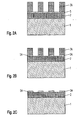
- a substrate 1 to be structured is provided, which may, for example, be a chip or wafer in which a matrix-shaped arrangement of trench capacitors has already been processed, which are each associated with memory cells.
- isolation regions are to be generated between the trench capacitors. Since the sections to be removed for generating the isolation regions also each contain subsections of the processed trench capacitors, silicon oxide also has to be etched, since the trench capacitors generally have an insulation collar made of silicon oxide.
- a carbon hard mask layer 2 is first applied on the thus pre-processed substrate 1.
- the production of the carbon hard mask layer 2 takes place as described by a plasma-assisted deposition process.
- there is generally a topographical structure in which it is advantageous to choose an HDP method for the deposition of the carbon hard mask layer 2, so that the carbon fills in all existing trenches and holes without cavities.
- the thickness of the carbon hard mask layer 2 is in the range 50-300 nm.
- the hard mask layer 2 may be formed, for example, as a gradient layer such that it has a diamond-like structure only in a lower layer thickness section, but has optimum antireflective properties in an upper layer thickness section.
- the latter may indicate that the structure does not have a diamond-like structure, but a more graphitic structure with a certain higher hydrogen content.
- the big advantage of the HDP method compared to the PECVD method is that the parameters determining the structure of the layer to be deposited can be better varied during the layer deposition.
- a layer 3 of a positive photoresist is deposited on the structure produced.
- This photoresist layer 3 is then exposed by conventional exposure by means of a chromium mask 5, then the exposed areas so that resist areas 3A remain on the carbon / hard mask layer 2. The result is shown in Fig. 1B.
- the carbon hard mask layer 2 is opened, which can be carried out, for example, by an anisotropic dry etching process with an O 2 plasma in which the reinforced resist areas 3A act as an etching mask.
- the etching is initially performed only up to the surface of the substrate 1.
- mask areas 2A of the carbon hard mask layer which serve as an etching hard mask for the subsequent etching step on the substrate 1 are formed by this etching step. The result is shown in FIG. 1D.
- the actual patterning process of the substrate 1 is performed by an anisotropic dry etching step, in which the mask regions 2A serve as ⁇ tzhartmaske.
- the dry etching step can be carried out, for example, with an O 2 plasma.
- the mask regions 2A remain unetched substrate regions 1A in which, for example, in the abovementioned application of the generation of insulation regions, fully processed trench capacitors and breakdown transistors of memory cells can be arranged. The result is shown in FIG. 1E.
- the mask regions 2A can be removed by a simple stripping process with an O 2 plasma. This in the form of the substrate areas 1A structured substrate 1 is shown in FIG. 1F.
- the etched areas must be filled by a suitable insulation material in a later, not shown process step.
- FIGS. 1D-F can optionally be carried out successively in a single reaction chamber.
- a carbon hard mask layer 2 is deposited on a substrate 1 to be structured by a plasma-assisted deposition method according to the invention.
- the intermediate layer 5 must have a sufficient etch resistance in the etching of the carbon hard mask layer 2.
- the photoresist layer is then applied to the intermediate layer 5 and patterned so that masked regions 3A remain.
- the structure of the photoresist layer is then first transferred into the intermediate layer 5, so that masked regions 5A of the intermediate layer 5 result below the masked regions 3A of the photoresist layer.
- the SiON layer 5 can be used in a dry etching process with etching gases such as Ar, CHF3, CF4 or the like. be etched for example in a MERIE reactor. Also conceivable are ICP, ECR or other plasma etching reactors.
- the masked photoresist areas 3A are removed in a standard paint shop.
- the carbon hard mask layer 2 is patterned so that masked regions 2A are formed below the masked SiON regions 5A.
- This may preferably be carried out in a dry etching process in a MERIE reactor using O 2 and / or N 2 etching media. This etching can be performed with high selectivity to the masked SiON regions 5A.
- the photoresist can also be removed in-situ, so that the intermediate step of FIG. 2C is saved using the standard varnishing shaver.
- the substrate 1 is patterned by means of the masked carbon hard mask regions 2A, so that structured substrate regions 1A are formed.
Landscapes
- Engineering & Computer Science (AREA)
- Physics & Mathematics (AREA)
- General Physics & Mathematics (AREA)
- Microelectronics & Electronic Packaging (AREA)
- Condensed Matter Physics & Semiconductors (AREA)
- Manufacturing & Machinery (AREA)
- Computer Hardware Design (AREA)
- Power Engineering (AREA)
- Chemical & Material Sciences (AREA)
- Inorganic Chemistry (AREA)
- Chemical Kinetics & Catalysis (AREA)
- Plasma & Fusion (AREA)
- Drying Of Semiconductors (AREA)
- Crystals, And After-Treatments Of Crystals (AREA)
- Semiconductor Memories (AREA)
Description
Die vorliegende Erfindung bezieht sich generell auf das Gebiet der Strukturierungsverfahren für die Halbleitertechnologie, bei welchen eine Schicht an der Oberfläche eines Substrats strukturiert werden soll. Insbesondere betrifft die Erfindung dabei ein Strukturierungsverfahren nach dem Oberbegriff des Patentanspruchs 1.The present invention generally relates to the field of structuring methods for semiconductor technology in which a layer is to be patterned on the surface of a substrate. In particular, the invention relates to a structuring method according to the preamble of
Bei der Fertigung von Halbleiterbauelementen tritt häufig das Erfordernis auf, dass in einem Verfahrensschritt eine Strukturierung durch Ätzen durchgeführt werden muss, bei der die zu entfernenden Abschnitte mindestens teilweise durch ein Siliziumoxid oder Siliziumnitrid gebildet werden. Ein Beispiel hierfür ist die Herstellung von Halbleiterspeicherzellen, welche einen Grabenkondensator und einen Auswahltransistor aufweisen. Während der Grabenkondensator auf einer Seite mit dem Auswahltranistor elektrisch durch eine vergrabene Brücke ("buried strap") verbunden wird, wird auf der anderen Seite des Grabenkondensators ein Isolationsgebiet (STI, "shallow trench isolation") erzeugt, durch welches der Grabenkondensator von einer benachbarten Speicherzelle elektrisch isoliert wird. Die Erzeugung des STI-Isolationsgebiets erfolgt durch einen Strukturierungsschritt, bei welchem ein Oberflächenabschnitt entfernt wird, der durch einen Teilabschnitt des zuvor erzeugten Grabenkondensators gebildet wird. Dies bedeutet, dass nicht nur Silizium geätzt werden muss, sondern auch Siliziumoxid, da der Grabenkondensator in seinem oberen Abschnitt einen Isolationskragen aus Siliziumoxid aufweist. Da sich an der Oberfläche des zu entfernenden Abschnitts zumeist eine Siliziumnitridschicht befindet, muß somit durch den Ätzprozeß auch Siliziumnitrid geätzt werden können.In the fabrication of semiconductor devices, there is often a requirement that patterning by etching be performed in a process step in which the portions to be removed are at least partially formed by a silicon oxide or silicon nitride. An example of this is the production of semiconductor memory cells having a trench capacitor and a selection transistor. While the trench capacitor is electrically connected on one side to the selection transistor by a buried strap, a shallow trench isolation (STI) is produced on the other side of the trench capacitor, through which the trench capacitor from an adjacent one Memory cell is electrically isolated. The generation of the STI isolation region is performed by a patterning step in which a surface portion formed by a portion of the trench capacitor previously formed is removed. This means that not only silicon has to be etched, but also silicon oxide, since the trench capacitor has an insulation collar of silicon oxide in its upper section. Since most of the surface of the removed portion a silicon nitride layer is located, must thus be etched by the etching process and silicon nitride.
Bezüglich der Erzeugung von STI-Isolationsgebieten bei der Herstellung der genannten Speicherzellen wird beispielhaft auf die deutschen Offenlegungsschriften DE 199 41 148 A1 und DE 199 44 012 A1 verwiesen.With regard to the generation of STI isolation regions in the production of said memory cells, reference is made, by way of example, to German published patent applications DE 199 41 148 A1 and DE 199 44 012 A1.
Angesichts der lateralen Dimensionen des Grabenkondensators, die in der Größenordnung von 100 - 200 nm liegen, stellt der genannte Prozess der Erzeugung des STI-Isolationsgebiets höchste Anforderungen an die Lagegenauigkeit, Maßhaltigkeit und Flankensteilheit des anzuwendenden Ätzprozesses, da sich die zu erzeugende Flanke der zu ätzenden Vertiefung mit äu-ßerst geringem lateralem Lagefehler innerhalb des Grabenkondensators auf der der Leitungsbrücke abgewandten Seite befinden muss.In view of the lateral dimensions of the trench capacitor, which are on the order of 100-200 nm, the said process of generating the STI isolation region places the highest demands on the positional accuracy, dimensional accuracy and edge steepness of the etching process to be used, since the edge to be etched is the one to be etched Deepening with extremely low lateral positional error within the trench capacitor must be located on the side facing away from the line bridge.
Zur Erzeugung kleinster Strukturen auf der Halbleiteroberfläche als auch zur Einhaltung geringster Variationen der Strukturbreiten über den Chip, den Wafer oder das Los ist es notwendig, dass die Reflexion von Licht der Belichtungswellenlänge an der Waferoberfläche (Grenzfläche Photolack - Substrat) möglichst vollständig unterbunden wird, um störende Interferenzeffekte auszuschalten. Dies gilt besonders für Belichtungswellenlängen bei und unter 248 nm (193 nm, 157 nm) aufgrund der zunehmenden Reflektivität der Substrate. Weiterhin muss zur Erzielung einer möglichst großen Tiefenschärfe bei der Belichtung die zu belichtende Lackschicht einerseits möglichst dünn sein. Um die Strukturübertragung, insbesondere bei Kontaktlöchern, zu realisieren, ist jedoch angepaßt an die zu ätzende Schichtdicke eine ausreichende Maskendicke und/oder eine hohe Ätzresistenz der Maske (Selektivität der Maske) notwendig.In order to produce the smallest structures on the semiconductor surface as well as to maintain the smallest variations in the structure widths over the chip, the wafer or the lot, it is necessary that the reflection of light of the exposure wavelength at the wafer surface (photoresist-substrate interface) is prevented as completely as possible eliminate interfering interference effects. This is especially true for exposure wavelengths at and below 248 nm (193 nm, 157 nm) due to the increasing reflectivity of the substrates. Furthermore, in order to achieve the greatest possible depth of focus during the exposure, the lacquer layer to be exposed on the one hand has to be as thin as possible on the one hand. In order to realize the structure transfer, in particular with contact holes, however, adapted to the layer thickness to be etched, a sufficient mask thickness and / or a high etch resistance of the mask (selectivity of the mask) is necessary.
Diesem Problem kann durch die folgenden im Stand der Technik bekannten Verfahren begegnet werden, die sämtlich darauf beruhen, dass eine zusätzliche Hilfsschicht verwendet wird.This problem can be addressed by the following methods known in the art, all of which rely on using an additional auxiliary layer.
In der EP 0 492 253 A1 ist ein Photostrukturierungsverfahren beschrieben, bei welchem zwei Photoresistschichten verwendet werden. Eine obere, relativ dünne Photoresistschicht (Topresist) wird nach der Strukturierung mit einem siliziumhaltigen Agens resistent gegen Trockenätzen im Sauerstoffplasma gemacht. In diesem nachfolgenden Trockenätzschritt wird die Struktur des Topresists mit dem exakten Maß der für die Strukturierung verwendeten Maske und mit senkrechten Flanken in eine untere, relativ dicke Photoresistschicht (bottom resist) übertragen. In Folge der chemischen Verstärkung des strukturiertem Topresists hat dieses Verfahren die Bezeichnung CARL (Chemische Aufweitung von Resist Linien) erhalten. Der Bottomresist dient während der Ätzung des Substrats als eigentliche Maske. Der Bottomresist selbst muss anschließend in einem speziellen Ätzverfahren, beispielsweise mit O2 oder SO2 entfernt werden. Derartige Photoresistmasken haben insbesondere während der Ätzung von Kontaktlöchern mit sehr hohem Aspektverhältnis den entscheidenden Nachteil, dass sich die aus dem Resist während der Ätzung entstehenden Polymere nicht kontrollieren lassen. Dies kann für sehr kleine Strukturen zu einer starken Reduktion des Ätzprozessfensters führen.EP 0 492 253 A1 describes a photostructuring method in which two photoresist layers are used. An upper, relatively thin photoresist layer (top resist) is made resistant to dry etching in oxygen plasma after structuring with a silicon-containing agent. In this subsequent dry-etching step, the top-resist structure is transferred to a lower, relatively thick photoresist layer (bottom resist) with the exact amount of mask used for patterning and with vertical edges. As a result of the chemical amplification of the structured top resist, this process has been given the designation CARL (Chemical Expansion of Resist Lines). The bottom resist serves as the actual mask during the etching of the substrate. The bottom resist itself must then be removed in a special etching process, for example with O 2 or SO 2 . Such photoresist masks have the decisive disadvantage, in particular during the etching of contact holes with a very high aspect ratio, that the polymers resulting from the resist during the etching can not be controlled. This can lead to a strong reduction of the etching process window for very small structures.
Des Weiteren sind Verfahren bekannt, bei denen als Hilfsschicht eine sogenannte Hartmaske verwendet wird. In der Deutschen Patentschrift DE 195 04 434 C1 wird eine Photolackschicht auf einer Maskenschicht aus einem siliziumhaltigen Dielektrikum entsprechend einer vorgegebenen Struktur belichtet und unter Verwendung von Lösungsmittel strukturiert. Die Photolackschicht wird verwendet, um die Struktur in die Maskenschicht zu übertragen, wobei ein modifiziertes anisotropes Plasmaätzverfahren eingesetzt wird, bei welchem der chemische Anteil der Ätzung dominiert. Anschließend wird der Photolack entfernt und die strukturierte Maskenschicht kann als Maske für ein Trockenätzverfahren zur Strukturierung des Substrats verwendet werden. Es sind ferner ähnliche Verfahren bekannt, bei denen Hartmasken aus Polysilizium eingesetzt werden. Die Polysilizium-Hartmaskenschicht wird dabei in einem Ofenprozess bei Temperaturen zwischen 600° C und 700° C abgeschieden, wodurch Probleme aufgrund der Wärmebelastung der bereits erzeugten Schaltungsstrukturen resultieren können. Ein generelles Problem der eben genannten Hartmaskenmaterialien liegt darin, dass sie in einem speziellen Ätzschritt geöffnet werden müssen. Ein weiterer Nachteil liegt darin, dass sie zumeist - wie bei dem Beispiel Polysilizium - nicht als antireflektierende Schichten tauglich sind.Furthermore, methods are known in which a so-called hard mask is used as the auxiliary layer. In the German patent DE 195 04 434 C1, a photoresist layer is exposed on a mask layer of a silicon-containing dielectric according to a predetermined structure and patterned using solvent. The photoresist layer is used to transfer the structure into the mask layer using a modified anisotropic plasma etching process in which the chemical portion of the etch is dominant. Subsequently, the photoresist and the patterned mask layer may be used as a mask for a dry etching process to pattern the substrate. There are also known similar methods in which hardmasks made of polysilicon are used. The Polysilicon hard mask layer is thereby deposited in a furnace process at temperatures between 600 ° C and 700 ° C, which may cause problems due to the heat load of the circuit structures already generated. A general problem of the aforementioned hard mask materials is that they must be opened in a special etching step. Another disadvantage is that they are mostly - as in the example polysilicon - not suitable as anti-reflective layers.
Bislang sind antireflektierende organische Schichten bekannt, die durch Aufschleuderverfahren vor der eigentlichen Belackung mit dem zu belichtenden Photoresist mit einem Track auf die Oberfläche des Wafers gebracht werden. Diese Schichten können jedoch nicht als Hartmaskenschichten verwendet werden und die Reflexion lässt sich auch nur bis auf ca. 10 % reduzieren. Des Weiteren sind anorganische Oxynitride, die mit einem CVD-Verfahren aufgebracht werden, als antireflektierende Schichten bekannt, wobei sich die Reflexion nicht unter 10 % reduzieren lässt. Zumindest für den Einsatz bei Oxidätzprozessen sind diese Schichten ebenfalls nicht als Hartmaskenschichten tauglich.So far, anti-reflective organic layers are known, which are brought by spin coating method before the actual coating with the exposed photoresist with a track on the surface of the wafer. However, these layers can not be used as hard mask layers and the reflection can only be reduced to about 10%. Furthermore, inorganic oxynitrides which are applied by a CVD method are known as antireflecting layers, whereby the reflection can not be reduced below 10%. At least for use in oxide etching processes, these layers are also not suitable as hard mask layers.
Es ist weiterhin aus den Druckschriften US-PS 5,378,316, US-PS 5,656,128 und EP 0 808 481 B1 bekannt, zur photolithographischen Strukturerzeugung eine Hartmaskenschicht aus Kohlenstoff einzusetzen. Es wird darin vorgeschlagen, die Kohlenstoff-Hartmaskenschicht durch ein PECVD (plasma enhanced chemical vapor deposition)-Verfahren abzuscheiden, wodurch gezielt Wasserstoff in die Kohlenstoffschicht eingebaut werden kann. Bei diesem Verfahren werden üblicherweise Drücke von ca. 133,3 - 1333 Pa des Plasmas in der Reaktorkammer und Substrattemperaturen um die 400° C eingestellt. Durch die PECVD-Abscheidung entsteht eine hoch verdichtete antireflektierende Schicht, die bereits recht gute Eigenschaften als Hartmaske aufweist und deren Brechungsindizes durch das Verfahren einstellbar sind. Damit ist ein Abgleich zwischen optischem Verhalten und Ätzresistenz möglich. Die Herstellung der Kohlenstoff-Hartmaskenschicht durch das PECVD-Verfahren liefert gute Ergebnisse, solange die Abscheidung auf planaren Strukturen erfolgen kann. Wenn die Abscheidung jedoch auf einer topografischen Struktur zu erfolgen hat, welche Löcher, Gräben oder Erhebungen aufweist, so beinhaltet das PECVD-Verfahren den Nachteil, dass die Kohlenstoffschicht nicht optimal in die Gräben und Löcher eingefüllt wird und zudem auch keine planarisierende Wirkung aufweist. Ein weiterer Nachteil ist, dass im allgemeinen die Hartmaskenqualität der Kohlenstoff-Hartmaskenschicht mit zunehmender Härte, d.h. zunehmenden Diamantanteil, in der Schicht und mit sinkendem Wasserstoffgehalt zunimmt, beide Kriterien jedoch mit dem PECVD-Verfahren nur begrenzt realisierbar sind. So ist der Diamantanteil der mit PECVD abgeschiedenen Schichten nahezu Null und der Wasserstoffgehalt kann nicht unter 15% gedrückt werden.It is furthermore known from the documents US Pat. No. 5,378,316, US Pat. No. 5,656,128 and EP 0 808 481 B1 to use a hard mask layer made of carbon for photolithographic structure generation. It is proposed therein to deposit the carbon hard mask layer by a PECVD (plasma-enhanced chemical vapor deposition) method, whereby hydrogen can be selectively incorporated into the carbon layer. In this method, pressures of about 133.3 - 1333 Pa of plasma in the reactor chamber and substrate temperatures around 400 ° C are usually set. By the PECVD deposition results in a highly compressed antireflecting layer, which already has quite good properties as a hard mask and whose refractive indices can be adjusted by the method. This allows a comparison between optical behavior and etch resistance. The preparation of the carbon hard mask layer by the PECVD method gives good results as long as the deposition can be done on planar structures. However, if the deposition is to be made on a topographical structure having holes, trenches or protrusions, the PECVD method involves the disadvantage that the carbon layer is not optimally filled in the trenches and holes and also has no planarizing effect. Another disadvantage is that in general the hardmask quality of the carbon hardmask layer increases with increasing hardness, ie increasing diamond content, in the layer and with decreasing hydrogen content, but both criteria can only be realized to a limited extent with the PECVD process. For example, the diamond content of layers deposited with PECVD is nearly zero and the hydrogen content can not be reduced below 15%.
Aus der bereits genannten US-PS 5,378,316 ist zudem bekannt, die Kohlenstoff-Hartmaskenschicht nicht direkt über den Photolack zu strukturieren, sondern über eine aus SiO2 gefertigte Zwischenschicht. Dies hat den Vorteil, dass die Photolackschicht dünner ausgeführt werden kann, wodurch ein größerer Spielraum bei der Einstellung der Prozeßbedingungen der Lithographie bei der Strukturierung des Photolacks gewonnen werden kann.From the aforementioned US Pat. No. 5,378,316 it is also known not to structure the carbon hard mask layer directly over the photoresist, but via an intermediate layer made of SiO 2 . This has the advantage that the photoresist layer can be made thinner, whereby a greater latitude in the adjustment of the process conditions of the lithography in the structuring of the photoresist can be obtained.
In der US-PS 5,981,398 wird ein Strukturierungsverfahren mit einem chlorhaltigen Plasma unter Verwendung einer Hartmaske beschrieben. Als Hartmaskenmaterial wird unter anderem eine amorphe Kohlenstoffschicht beschrieben, die durch ein HDP-(high density plasma)CVD-Verfahren hergestellt wird. Die darin beschriebenen Ätzprozesse dienen der Herstellung und Strukturierung von elektrisch leitfähigen Materialien, insbesondere (A1-) Leiterbahnmaterialien. Es wird jedoch nicht genauer beschrieben, wie die Prozessführung erfolgen soll, damit eine Kohlenstoff-Hartmaskenschicht hoher Qualität erzielt werden kann.US Pat. No. 5,981,398 describes a structuring process using a chlorine-containing plasma using a hard mask. As hard mask material, inter alia, an amorphous carbon layer is described, which is produced by a HDP (high density plasma) CVD method. The etching processes described therein serve for the production and structuring of electrically conductive materials, in particular (A1-) trace materials. However, it is not described in more detail how the process is to be carried out so that a high-quality carbon hard mask layer can be obtained.
Es ist demzufolge Aufgabe der vorliegenden Erfindung, ein verbessertes Herstellungsverfahren für eine Kohlenstoff-Hartmaskenschicht anzugeben, mit welchem die Schicht einerseits auf jeder beliebigen Topographie abgeschieden werden kann und andererseits die Schichteigenschaften besser zwischen optimalen antireflektierenden Eigenschaften und optimalen Ätzresistenzeigenschaften eingestellt werden können.It is accordingly an object of the present invention to provide an improved method for producing a carbon hard mask layer, with which the layer on the one hand can be deposited on any topography and on the other hand, the layer properties can be better adjusted between optimal antireflective properties and optimal Ätzresistenzeigenschaften.
Diese Aufgabe wird durch die kennzeichnenden Merkmale des Patentanspruchs 1 gelöst. Vorteilhafte Weiterbildungen und Ausgestaltungen sind in den Unteransprüchen angegeben.This object is solved by the characterizing features of
Ein wesentlicher Gedanke der Erfindung besteht darin, die Kohlenstoff-Hartmaskenschicht durch ein plasmaunterstütztes Abscheideverfahren abzuscheiden und die Abscheidung derart durchzuführen, dass die Kohlenstoff-Hartmaskenschicht in mindestens einem Schichtdickenabschnitt eine einem Diamanten vergleichbare Härte aufweist.An essential idea of the invention is to deposit the carbon hard mask layer by a plasma-assisted deposition method and to carry out the deposition in such a way that the carbon hard mask layer has a hardness comparable to a diamond in at least one layer thickness section.
Dabei kann vorgesehen sein, dass sich der genannte Schichtdickenabschnitt über die gesamte Kohlenstoff-Hartmaskenschicht erstreckt und somit die Kohlenstoff-Hartmaskenschicht über ihre gesamte Dicke optimale diamantähnliche Härteeigenschaften und Ätzresistenzeigenschaften aufweist. Es ist aber ebenso möglich, dass die Schicht nur in einem begrenzten Schichtdickenabschnitt eine diamantähnliche Härte aufweist und in den übrigen Schichtdickenabschnitten eine davon abweichende Härte aufweist.It may be provided that the said layer thickness section extends over the entire carbon hard mask layer and thus the carbon hard mask layer has optimum diamond-like hardness properties and etching resistance properties over its entire thickness. However, it is also possible that the layer has a diamond-like hardness only in a limited layer thickness section and has a different hardness in the remaining layer thickness sections.
Wenn im folgenden des öfteren die Termini "diamantartig" oder "graphitartig" verwendet werden, so bezieht sich dies nicht notwendigerweise auf die Struktur der aufgebrachten Schicht. Auch wenn die Schicht mit diamantartiger Härte aufgebracht wird, so kann und wird die Kristallstruktur in der Regel eine amorphe Kohlenstoffstruktur sein.If, in the following, the terms "diamond-like" or "graphite-like" are used frequently, this does not apply necessarily on the structure of the applied layer. Even if the layer of diamond-like hardness is applied, the crystal structure can and will usually be an amorphous carbon structure.
Bei der Erzeugung des diamantartigen Schichtdickenabschnitts werden erfindungsgemäß die Parameter bei der Abscheidung derart eingestellt, dass graphitartig entstehende Bereiche durch nachfolgende Ätzprozesse in-situ wieder entfernt werden und dass nur diamantartig entstehende Bereiche bestehen bleiben. Solche die Ätzprozesse fördernden Parameter sind beispielsweise die Zufuhr ionisierbarer Gase wie Argon und/oder Neon in die Reaktorkammer, durch die ein zusätzlicher Ionenbeschuss bei der Abscheidung herbeigeführt wird. Ein weiterer die Ätzprozesse fördernder Parameter ist der Wasserstoffanteil in der Gasphase.In the production of the diamond-like layer thickness section, the parameters are set according to the invention in the deposition such that regions resulting graphitically are removed again in situ by subsequent etching processes and that only areas that arise like diamonds remain. Such parameters which promote the etching processes are, for example, the supply of ionizable gases such as argon and / or neon into the reactor chamber, by means of which additional ion bombardment is brought about in the deposition. Another parameter promoting the etching processes is the hydrogen content in the gas phase.
Diese Parameter können während dem Schichtwachstum variiert werden, so dass die entstehende Kohlenstoff-Hartmaskenschicht über ihre Schichtdicke in ihren Eigenschaften verändert werden kann.These parameters can be varied during the layer growth, so that the resulting carbon hard mask layer can be changed in its properties via its layer thickness.
Der Strukturierungsprozess kann so erfolgen, dass auf das zu strukturierende Substrat zunächst eine Kohlenstoff-Hartmaskenschicht wie angegeben aufgebracht und anschließend auf die Kohlenstoff-Hartmaskenschicht eine Photoresistschicht aufgebracht wird. Nach dem Belichten und Entwickeln der Photoresistschicht zur Erzeugung einer vorgegebenen Struktur wird diese Struktur in die Kohlenstoff-Hartmaskenschicht übertragen. Die Kohlenstoff-Hartmaskenschicht dient dann als eigentliche Ätzmaske zum Ätzen des Substrats.The structuring process can be carried out by first applying a carbon hard mask layer to the substrate to be structured as indicated, and then applying a photoresist layer to the carbon hard mask layer. After exposing and developing the photoresist layer to form a predetermined pattern, this structure is transferred into the carbon hardmask layer. The carbon hard mask layer then serves as the actual etching mask for etching the substrate.
Es kann ebenso vorgesehen sein, dass die Kohlenstoff-Hartmaskenschicht über eine ätzresistente Zwischenschicht strukturiert wird, die beispielsweise durch eine Siliziumoxidnitridschicht gebildet sein kann.It may also be provided that the carbon hard mask layer is patterned via an etch-resistant intermediate layer, which may be formed, for example, by a silicon oxide nitride layer.
Als Abscheideverfahren kann vorteilhaft ein sogenanntes HDP-(high density plasma) Abscheideverfahren verwendet werden. Dies erweist sich insbesondere dann als vorteilhaft, wenn die Kohlenstoff-Hartmaskenschicht auf einer topographischen Struktur erzeugt werden soll, da sich gerade bei der Wahl dieses Abscheideverfahrens der Kohlenstoff besonders gut lunkerfrei in Löcher und Gräben eingefüllt werden kann.As a deposition method, a so-called HDP (high density plasma) deposition method can be advantageously used. This proves to be particularly advantageous if the carbon hard mask layer on a topographic Structure is to be produced, since just in the choice of this deposition process, the carbon can be filled very well void-free in holes and trenches.
Die HDP-Abscheidung kann beispielsweise bei Drücken von ca. 0,133 - 26,6 Pa durchgeführt werden und die Substrattemperatur kann in einem Bereich zwischen 200° C - 750° C, vorzugsweise 600°C - 750°C, geregelt werden.For example, the HDP deposition may be performed at pressures of about 0.133 - 26.6 Pa and the substrate temperature may be controlled in a range between 200 ° C - 750 ° C, preferably 600 ° C - 750 ° C.
Im übrigen sind für das HDP-Verfahren die in der DE 199 04 311 A1 enthaltenen Angaben maßgebend.Moreover, the information contained in DE 199 04 311 A1 is decisive for the HDP process.
Ein HDP-Reaktor zur Erzeugung eines hochdichten Plasmas umfaßt eine zentrale Kammer, in der Halbleiter- oder Isolatorsubstrate auf einem Boot sitzen, das die Substrate nicht beeinträchtigt oder irgendwelche Verunreinigungen in die Substrate einführt. Die zentrale Kammer besteht aus einem Material, das Drücken um 0.133 Pa (1 mTorr) oder weniger widerstehen kann, bei derartigen Drücken minimal ausgast und zu keinen Verunreinigungen Anlaß gibt, die in das Innere der Kammer oder in die Substrate oder in einen darauf befindlichen Dünnfilm eindringen. Die zentrale Kammer arbeitet bei einem Betriebsdruck, der sehr viel niedriger als bei üblichen Kammern für chemische Abscheidung aus der Gasphase oder plasmagestützte chemische Abscheidung aus der Gasphase ist. Der Druck inner-halb der Kammer beträgt vorzugsweise etwa 0.67 Pa (5 mTorr), während bei der plasmagestützten chemischen Abscheidung aus der Gas-phase typischerweise ein Druck von etwa 267 Pa (2 Torr) verwendet wird. Die Plasmadichte innerhalb der Kammer ist viel höher als bei der normalen chemischen Abscheidung aus der Gasphase, selbst wenn sie plasmagestützt ist, und liegt vorzugsweise über 1016 Ionen/m3, vorzugsweise im Bereich von 1016 bis 1022 und insbesondere im Bereich von 1017 bis 1019 Ionen/m3. Die Plasmadichte könnte aber auch noch höher sein. Im Vergleich hierzu liegt beim typischen Betriebsdruck einer Kammer zur plasmagestützten chemischen Abscheidung aus der Gasphase die Plasmadichte im Bereich von 1014 bis 1016 Ionen/m3.An HDP reactor for producing a high density plasma includes a central chamber in which semiconductor or insulator substrates sit on a boat that does not interfere with the substrates or introduce any contaminants into the substrates. The central chamber is made of a material that can withstand pressures less than or equal to 1 mTorr or less, at such pressures, minimizing outgassing and no impurities entering the interior of the chamber or into the substrates or a thin film thereon penetration. The central chamber operates at an operating pressure much lower than conventional gas phase chemical vapor deposition chambers or plasma enhanced chemical vapor deposition. Preferably, the pressure within the chamber is about 0.67 Pa (5 mTorr), while plasma assisted chemical vapor deposition typically uses a pressure of about 267 Pa (2 Torr). The plasma density within the chamber is much higher than the normal chemical vapor deposition, even when plasma enhanced, and is preferably above 10 16 ions / m 3 , preferably in the range of 10 16 to 10 22, and more preferably in the range of 10 17 to 10 19 ions / m 3 . The plasma density could be even higher. By comparison, at the typical operating pressure of a chamber for plasma-assisted chemical vapor deposition, the plasma density is in the range of 10 14 to 10 16 ions / m 3 .
Ein Charakteristikum des erfindungsgemäßen Verfahrens ist, dass der Materialabscheidung eine Ionensputterätzung überlagert wird. Diese sollte beitragsmäßig so groß sein, dass sich wie bereits angedeutet ein Wachstumsselektionsprozeß herausbildet. Zu diesem Zweck kann die Schicht mit Ar-Ionen, Ne-Ionen oder auch anderen Ionen gesputtert werden. Als Kohlenstoffprekursor sind Gase wie CH4 , C2H6, C2H4, C2H2 und C3H6 geeignet. Weiterhin vorteilhaft für die Schichtbildung ist das Zufügen relativ großer Anteile an Wasserstoff. Mit zunehmenden Ionenbeschuß und zunehmenden Wasserstoffanteil in der Gasphase werden die erzeugten Kohlenstoffschichten härter, weil beide Parameter ein Ätzen der graphitartigen Anteile in der Kohlenstoffschicht bedingen, wobei die gleichzeitig vorliegenden Diamantanteile nicht zurückgeätzt werden, da sie diesem Angriff gegenüber resistenter sind. Die so gebildete Schicht ist resistenter gegenüber Ionen-Ätzprozessen und ergibt mithin eine Hartmaske höherer Qualität. Gleichzeitig ermöglicht der simultane Abscheide-Sputterprozess ein Auffüllen von Gräben oder Löchern auf strukturierten Oberflächen. Die durch das HDP-Verfahren abgeschiedene Kohlenstoffschicht weist einen niedrigeren Wasserstoffgehalt als die durch das PECVD-Verfahren abgeschiedene Kohlenstoffschicht auf. Insbesondere kann durch geeignete Einstellung der Parameter der Wasserstoffanteil auf unter 5 % gedrückt werden. Die Kohlenstoffschicht füllt sich lunkerfrei in kleinste Strukturen mit Durchmessern unterhalb von 100 nm und ist in der Lage, Topographien zu planarisieren.A characteristic of the method according to the invention is that the material deposition is superimposed on an ion sputter etching. This contribution should be so large that, as already indicated, a growth selection process is emerging. For this purpose, the layer can be sputtered with Ar ions, Ne ions or other ions. Suitable carbon precursors are gases such as CH 4 , C 2 H 6 , C 2 H 4 , C 2 H 2 and C 3 H 6 . Also advantageous for the formation of layers is the addition of relatively large amounts of hydrogen. With increasing ion bombardment and increasing hydrogen content in the gas phase, the carbon layers produced become harder, because both parameters require etching of the graphite-like portions in the carbon layer, whereby the simultaneously present diamond portions are not etched back because they are more resistant to this attack. The layer thus formed is more resistant to ion etching processes and thus gives a higher quality hardmask. At the same time, the simultaneous deposition-sputtering process enables filling of trenches or holes on structured surfaces. The carbon layer deposited by the HDP method has a lower hydrogen content than the carbon layer deposited by the PECVD method. In particular, by appropriate adjustment of the parameters, the hydrogen content can be reduced to less than 5%. The carbon layer fills without cavities in the smallest structures with diameters below 100 nm and is able to planarize topographies.
Sowohl der Ionenbeschuss als auch die Substrattemperatur können während der Abscheidung gezielt variiert werden. Dadurch wird die Bildung sogenannter Gradientenschichten möglich, d.h. mit der Schichttiefe können die optischen Eigenschaften und auch die mechanischen Eigenschaften verändert werden. Dadurch werden optimale antireflektierende Schichten erzeugt, da eine Veränderung des Brechungsindex mit der Schichttiefe eine maximale Reflexionsminderung bedeutet. Gleichzeitig kann der Prozess so gestaltet werden, dass die Härte beispielsweise in den untersten Schichtbereichen größer ist als an der Schichtoberfläche. Das ermöglicht eine optimale Prozessführung beim nachfolgenden Trockenätzprozess.Both the ion bombardment and the substrate temperature can be selectively varied during the deposition. Thereby the formation of so-called gradient layers is possible, ie with the layer depth, the optical properties and also the mechanical properties can be changed. As a result, optimal antireflecting layers are produced, since a change in the refractive index with the layer depth means a maximum reflection reduction. At the same time, the process can be designed so that the hardness is greater, for example, in the lowest layer areas than at the layer surface. This enables optimal process control during the subsequent dry etching process.
Gegebenenfalls kann als Abscheideverfahren auch ein PECVD-(plasma enhanced chemical vapor deposition) Abscheideverfahren gewählt werden. Dabei ist Voraussetzung, dass diejenige Elektrode des üblicherweise verwendeten Parallelplattenreaktors, auf der die Substrate angeordnet sind, als Kathode geschaltet wird. In diesem Fall wird ein Teil der aufwachsenden Schicht durch die Ionen wieder weggesputtert. Um erfindungsgemäß einen Wachstumsselektionsprozeß herbeizuführen, können wie beim HDP-Abscheideverfahren Elemente wie Argon, Neon u.a. zur Bildung entsprechender Ionen in verstärktem Maße dem Reaktor zugeführt werden.Optionally, as a deposition method, a PECVD (plasma enhanced chemical vapor deposition) deposition method can be selected. It is a prerequisite that the electrode of the commonly used parallel plate reactor, on which the substrates are arranged, is connected as a cathode. In this case, part of the growing layer is sputtered away by the ions again. In order to bring about a growth selection process according to the invention, elements such as argon, neon and the like can be used as in the HDP deposition process. be supplied to the reactor to a greater extent to form corresponding ions.
Gewünschtenfalls kann das beschriebene Verfahren der Verwendung einer Kohlenstoff-Hartmaskenschicht auch mit dem eingangs beschriebenen CARL-Prozess kombiniert werden, bei welchem eine chemische Verstärkung der Resistlinien der Photoresistschicht herbeigeführt wird. Diese chemische Verstärkung kann beispielsweise durch eine nasschemische Silylierung, also die Anlagerung von Silyl-Gruppen an das organische Resistmaterial bewirkt werden, wie es beispielsweise in den Druckschriften DE 42 26 464, EP 0 395 917 oder US-5,234,793 beschrieben worden ist.If desired, the described method of using a carbon hardmask layer can also be combined with the CARL process described in the introduction, in which chemical amplification of the photoresist layer resist lines is brought about. This chemical amplification can be effected, for example, by a wet-chemical silylation, that is to say the addition of silyl groups to the organic resist material, as has been described, for example, in the publications DE 42 26 464, EP 0 395 917 or US Pat. No. 5,234,793.
Das erfindungsgemäße Verfahren eignet sich insbesondere zur Erzeugung der bereits eingangs beschriebenen Grabenisolation in der Herstellung von Speicherzellen mit Grabenkondensator und Auswahltransistor durch den sogenannten AA-Prozess (active area). Für diesen Prozess wird derzeit eine Borsilikatglas-Hartmaske als Ätzmaske verwendet, was aus verschiedenen Gründen keine optimale Lösung ist.The method according to the invention is particularly suitable for producing the trench isolation already described above in the production of memory cells with trench capacitor and selection transistor by the so-called AA process (active area). For this process, a borosilicate glass hard mask is currently being used as an etching mask, which for various reasons is not an optimal solution.
Nachfolgend wird ein Ausführungsbeispiel der Durchführung des erfindungsgemäßen Verfahren in Verbindung mit den Zeichnungsfiguren näher erläutert. Es zeigen:
- Fig. 1 A - F verschiedene Stadien bei der Strukturierung eines Substrats nach einer ersten Ausführungsart des erfindungsgemäßen Verfahrens unter Verwendung chemischer Resistverstärkung;
- Fig.2A-E verschiedene Stadien bei der Strukturierung eines Substrats nach einer zweiten Ausführungsart des erfindungsgemäßen Verfahrens unter Verwendung einer ätzresistenten Zwischenschicht.
- FIGS. 1A-F show various stages in the patterning of a substrate according to a first embodiment of the method according to the invention using chemical resist amplification;
- 2A-E different stages in the structuring of a substrate according to a second embodiment of the method according to the invention using an etch-resistant intermediate layer.
Gemäß Fig. 1A wird zunächst ein zu strukturierendes Substrat 1 bereitgestellt, bei welchem es sich beispielsweise um einen Chip bzw. Wafer handeln kann, in welchen bereits eine matrixförmige Anordnung aus Grabenkondensatoren prozessiert worden ist, die jeweils Speicherzellen zugehörig sind. Durch den hier im folgenden beispielhaft dargestellten Strukturierungsprozess sollen zwischen den Grabenkondensatoren Isolationsgebiete (STI) erzeugt werden. Da die zur Erzeugung der Isolationsgebiete zu entfernenden Abschnitte auch jeweils Teilabschnitte der prozessierten Grabenkondensatoren enthalten, muss demzufolge auch Siliziumoxid geätzt werden, da die Grabenkondensatoren im allgemeinen einen aus Siliziumoxid bestehenden Isolationskragen aufweisen.According to FIG. 1A, first of all a
Auf dem solchermaßen vorprozessierten Substrat 1 wird nun zunächst eine Kohlenstoff-Hartmaskenschicht 2 aufgebracht. Die Erzeugung der Kohlenstoff-Hartmaskenschicht 2 erfolgt wie beschrieben durch ein plasmaunterstütztes Abscheideverfahren. Bei dem genannten Anwendungsfall der Vorbereitung von Isolationsgebieten liegt im allgemeinen eine topographische Struktur vor, bei der es vorteilhaft ist, für die Abscheidung der Kohlenstoff-Hartmaskenschicht 2 ein HDP-Verfahren zu wählen, damit sich der Kohlenstoff lunkerfrei in alle vorhandenen Gräben und Löcher einfüllt. Die Dicke der Kohlenstoff-Hartmaskenschicht 2 liegt im Bereich 50 - 300 nm.On the thus
Durch das erfindungsgemässe Verfahren wird es darüber hinaus möglich, die Kohlenstoff-Hartmaskenschicht 2 prozessangepasst mit optimalen schichtdickenabhängigen Eigenschaften herzustellen. Die Hartmaskenschicht 2 kann beispielsweise als Gradientenschicht derart ausgebildet sein, dass sie nur in einem unteren Schichtdickenabschnitt diamantartige Struktur aufweist, in einem oberen Schichtdickenabschnitt jedoch optimale antireflektierende Eigenschaften aufweist. Letztere bedingen möglicherweise, dass die Struktur keine diamantartige Struktur, sondern eine mehr graphitartige Struktur mit einem bestimmten höheren Wasserstoffanteil aufweist. Der grosse Vorteil des HDP-Verfahrens gegenüber dem PECVD-Verfahren liegt darin, dass sich die die Struktur der abzuscheidenden Schicht bestimmenden Parameter während der Schichtabscheidung besser variieren lassen. Wenn ein Übergang von einer amorphen, graphitartigen Struktur zu einer diamantartigen Struktur erzeugt werden soll, so muß beispielsweise nur der Anteil des zugeführten Wasserstoffs und/oder der Anteil zusätzlicher ionisierbarer Gase wie Argon oder Neon auf einen bestimmten Wert gesteigert werden. Durch die dann zunehmenden Ätzprozesse kann die Struktur nicht mehr graphitartig aufwachsen, so dass nur noch die diamantartig entstehenden Strukturen von Bestand sind.Moreover, it is possible by means of the method according to the invention to produce the carbon hard mask layer 2 in a process-adapted manner with optimum layer thickness-dependent properties. The hard mask layer 2 may be formed, for example, as a gradient layer such that it has a diamond-like structure only in a lower layer thickness section, but has optimum antireflective properties in an upper layer thickness section. The latter may indicate that the structure does not have a diamond-like structure, but a more graphitic structure with a certain higher hydrogen content. The big advantage of the HDP method compared to the PECVD method is that the parameters determining the structure of the layer to be deposited can be better varied during the layer deposition. For example, if a transition from an amorphous, graphitic structure to a diamond-like structure is to be generated, then only the proportion of hydrogen introduced and / or the proportion of additional ionizable gases, such as argon or neon, must be increased to a particular value. As a result of the increasing etching processes, the structure can no longer grow up graphitically, so that only the diamond-like structures are retained.
Anschließend wird auf die erzeugte Struktur eine Schicht 3 eines positiven Photoresists abgeschieden. Diese Photoresistschicht 3 wird dann durch konventionelle Belichtung mittels einer Chrommaske 5 belichtet, anschließend werden die belichteten Bereiche entfernt, so dass Resistbereiche 3A auf der Kohlenstoff-/Hartmaskenschicht 2 zurückbleiben. Das Ergebnis ist in Fig. 1B dargestellt.Subsequently, a
Anschließend wird eine chemische Verstärkung der Resistbereiche 3A durch eine nasschemische Silylierung durchgeführt, bei welcher sich Silyl-Gruppen an das organische Material der Photoresistbereiche 3A anlagern, so dass um die Resistbereiche 3A Verstärkungsbereiche 4A aus Silyl-Gruppen gebildet werden. Das Ergebnis ist in der Fig. 1C dargestellt.Subsequently, chemical amplification of the resist
Im nächsten Schritt erfolgt die Öffnung der Kohlenstoff-Hartmaskenschicht 2, die beispielsweise durch einen anisotropen Trockenätzprozess mit einen O2-Plasma durchgeführt werden kann, bei welchem die verstärkten Resistbereiche 3A als Ätzmaske wirken. Die Ätzung wird zunächst nur bis zu der Oberfläche des Substrats 1 durchgeführt. Unterhalb der verstärkten Resistbereiche 3A entstehen durch diesen Ätzschritt Maskenbereiche 2A der Kohlenstoff-Hartmaskenschicht, die für den nachfolgenden Ätzschritt an dem Substrat 1 als Ätzhartmaske dienen. Das Ergebnis ist in der Fig. 1D dargestellt.In the next step, the carbon hard mask layer 2 is opened, which can be carried out, for example, by an anisotropic dry etching process with an O 2 plasma in which the reinforced resist
Anschließend wird der eigentliche Strukturierungsprozess des Substrats 1 durch einen anisotropen Trockenätzschritt durchgeführt, bei welchem die Maskenbereiche 2A als Ätzhartmaske dienen. Der Trockenätzschritt kann beispielsweise mit einem O2-Plasma erfolgen. Unterhalb der Maskenbereiche 2A verbleiben ungeätzte Substratbereiche 1A, in denen beispielsweise in dem obengenannten Anwendungsfall der Erzeugung von Isolationsgebieten fertig prozessierte Grabenkondensatoren und Ausfalltransistoren von Speicherzellen angeordnet sein können. Das Ergebnis ist in der Fig. 1E dargestellt.Subsequently, the actual patterning process of the
Schließlich können in einem letzten Verfahrensschritt die Maskenbereiche 2A durch einen einfachen Stripping-Prozess mit einem O2-Plasma entfernt werden. Das in Form der Substratbereiche 1A strukturierte Substrat 1 ist in der Fig. 1F dargestellt.Finally, in a final process step, the
Für die Erzeugung von Isolationsbereichen müssen in einem späteren, nicht dargestellten Verfahrensschritt die freigeätzten Bereiche durch ein geeignetes Isolationsmaterial aufgefüllt werden.For the production of insulation areas, the etched areas must be filled by a suitable insulation material in a later, not shown process step.
Die in den Fig. 1D-F dargestellten Verfahrensschritte können gegebenenfalls in einer einzigen Reaktionskammer nacheinander durchgeführt werden.The process steps illustrated in FIGS. 1D-F can optionally be carried out successively in a single reaction chamber.
Gemäß Fig.2A wird auf ein zu strukturierendes Substrat 1 nach einem erfindungsgemäßen plasmaunterstützten Abscheideverfahren eine Kohlenstoff-Hartmaskenschicht 2 abgeschieden. Auf diese wird dann beispielsweise durch ein PECVD-Verfahren eine ätzresistente Zwischenschicht 5 aufgebracht, die beispielsweise durch eine ca. 25 nm dicke Siliziumoxidnitrid (SiON) gebildet sein kann. Die Zwischenschicht 5 muß eine ausreichende Ätzresistenz bei der Ätzung der Kohlenstoff-Hartmaskenschicht 2 aufweisen. Auf die Zwischenschicht 5 wird dann die Photoresistschicht aufgebracht und strukturiert, so dass maskierte Bereiche 3A stehenbleiben.According to FIG. 2A, a carbon hard mask layer 2 is deposited on a
Gemäß Fig.2B wird anschließend zunächst die Struktur der Photoresistschicht in die Zwischenschicht 5 übertragen, so dass maskierte Bereiche 5A der Zwischenschicht 5 unterhalb der maskierten Bereiche 3A der Photoresistschicht resultieren. Die SiON-Schicht 5 kann in einem Trockenätzprozeß mit Ätzgasen wie Ar, CHF3, CF4 o.ä. beispielsweise in einem MERIE-Reaktor geätzt werden. Denkbar sind ebenso ICP-, ECR- oder andere Plasmaätzreaktoren.According to FIG. 2B, the structure of the photoresist layer is then first transferred into the
Gemäß Fig.2C werden die maskierten Photoresistbereiche 3A in einem Standardlackierascher entfernt.According to Fig. 2C, the
Dann wird entsprechend Fig.2D die Kohlenstoff-Hartmaskenschicht 2 strukturiert, so dass maskierte Bereiche 2A unterhalb der maskierten SiON-Bereiche 5A gebildet werden. Dies kann vorzugsweise in einem Trockenätzprozeß in einem MERIE-Reaktor unter Verwendung von O2- und/oder N2-Ätzmedien durchgeführt werden. Diese Ätzung kann mit hoher Selektivität zu den maskierten SiON-Bereichen 5A durchgeführt werden. Hierbei kann auch in-situ der Photolack entfernt werden, so dass der Zwischenschritt der Fig.2C unter Verwendung des Standardlackieraschers eingespart wird.Then, according to FIG. 2D, the carbon hard mask layer 2 is patterned so that
Anschließend wird wie bereits in Verbindung mit Fig.1 beschrieben, das Substrat 1 mittels der maskierten Kohlenstoff-Hartmaskenbereiche 2A strukturiert, so dass strukturierte Substratbereiche 1A gebildet werden.Subsequently, as already described in connection with FIG. 1, the
Claims (12)
- Process for the photolithographic production of patterns in a substrate (1), in whicha) a carbon hard mask layer (2) is applied to the substrate (1) by a plasma-enhanced deposition process, the deposition being carried out in such a manner that the carbon hard mask layer (2), in at least one layer thickness section, has a hardness comparable to that of diamond,b) the carbon hard mask layer (2) is patterned, andc) the pattern of the carbon hard mask layer (2) is transferred to the substrate (1),characterized in that- in process step a), during the production of the diamond-like layer thickness section, the parameters used for the deposition are set in such a manner that graphite-like regions which are formed are removed again by subsequent etching processes, and in that regions with a diamond-like hardness which are formed are retained.
- Process according to Claim 1, characterized in that- additional ion bombardment is brought about during the deposition, in particular through the introduction of Ar and/or Ne, and/or- hydrogen is supplied.
- Process according to Claim 1 or 2, characterized in that- in process step a), one or more of the gases CH4, C2H6, C2H4, C2H2 and C3H6 are used as carbon precursor.
- Process according to one of the preceding claims,
characterized in that- an HDP deposition process is used in process step a). - Process according to one of the preceding claims,
characterized in that- a substrate temperature of from 200°C-750°C is set during the production of the diamond-like layer thickness section. - Process according to one of the preceding claims,
characterized in that- a PECVD deposition process is used in process step a). - Process according to one of the preceding claims,
characterized in that- in process step b), a photoresist layer (3) is applied to the carbon hard mask layer (2), is patterned by photolithography and the pattern is transferred to the carbon hard mask layer (2). - Process according to Claim 7, characterized in that- an interlayer (5) is introduced between the carbon hard mask layer (2) and the photoresist layer (3), and- the pattern produced in the photoresist layer (3) is transferred to the interlayer (5) and is then transferred to the carbon hard mask layer (2).
- Process according to Claim 7 or 8,
characterized in that- the photoresist layer (3) is chemically amplified after it has been patterned. - Process according to one of the preceding claims,
characterized in that- the carbon hard mask layer (2) is formed as a gradient layer. - Process according to Claim 10, characterized in that- the process step a) is carried out in such a manner that the composition and/or the pattern of the carbon hard mask layer (2) varies as a function of its depth.
- Process for producing insulation regions between components formed in a substrate (1), in which- the substrate is patterned as described in one or more of the above claims, and- the removed regions are filled with an insulating material.
Applications Claiming Priority (3)
| Application Number | Priority Date | Filing Date | Title |
|---|---|---|---|
| DE10153310 | 2001-10-29 | ||
| DE10153310A DE10153310A1 (en) | 2001-10-29 | 2001-10-29 | Photolithographic structuring process with a carbon hard mask layer produced by a plasma-assisted deposition process with diamond-like hardness |
| PCT/DE2002/004034 WO2003038875A2 (en) | 2001-10-29 | 2002-10-29 | Method for photolithographic structuring by means of a carbon hard mask layer which has a diamond-like hardness and is deposited by means of a plasma method |
Publications (2)
| Publication Number | Publication Date |
|---|---|
| EP1444724A2 EP1444724A2 (en) | 2004-08-11 |
| EP1444724B1 true EP1444724B1 (en) | 2007-01-24 |
Family
ID=7704081
Family Applications (1)
| Application Number | Title | Priority Date | Filing Date |
|---|---|---|---|
| EP02776865A Expired - Lifetime EP1444724B1 (en) | 2001-10-29 | 2002-10-29 | Method for photolithographic structuring by means of a carbon hard mask layer which has a diamond-like hardness and is produced by means of a plasma-enhanced deposition method |
Country Status (6)
| Country | Link |
|---|---|
| US (1) | US7368390B2 (en) |
| EP (1) | EP1444724B1 (en) |
| KR (1) | KR100592818B1 (en) |
| DE (2) | DE10153310A1 (en) |
| TW (1) | TW583518B (en) |
| WO (1) | WO2003038875A2 (en) |
Families Citing this family (40)
| Publication number | Priority date | Publication date | Assignee | Title |
|---|---|---|---|---|
| DE10231533A1 (en) * | 2002-07-11 | 2004-01-29 | Infineon Technologies Ag | Process for metal structuring |
| JP4223348B2 (en) * | 2003-07-31 | 2009-02-12 | Tdk株式会社 | Magnetic recording medium manufacturing method and manufacturing apparatus |
| US7129180B2 (en) | 2003-09-12 | 2006-10-31 | Micron Technology, Inc. | Masking structure having multiple layers including an amorphous carbon layer |
| US7132201B2 (en) | 2003-09-12 | 2006-11-07 | Micron Technology, Inc. | Transparent amorphous carbon structure in semiconductor devices |
| DE102004008497A1 (en) * | 2004-02-20 | 2005-09-08 | Infineon Technologies Ag | A manufacturing method for a semiconductor structure in a substrate, wherein the semiconductor structure has at least two areas to be differently structured |
| JP2006012332A (en) * | 2004-06-28 | 2006-01-12 | Tdk Corp | Dry etching method, method of manufacturing magnetic recording medium, and magnetic recording medium |
| DE102004031121A1 (en) * | 2004-06-28 | 2006-01-19 | Infineon Technologies Ag | Production of a layer arrangement, used in the manufacture of integrated circuits e.g. transistors, comprises forming a first conducting layer, a structuring auxiliary layer and a dielectric layer, and structuring the dielectric layer |
| KR100678460B1 (en) | 2004-10-12 | 2007-02-02 | 삼성전자주식회사 | Methods of forming a channel-portion hole between self-alignment patterns and methods of forming a semconductor devices having gate patterns by using thereof |
| US8664124B2 (en) | 2005-10-31 | 2014-03-04 | Novellus Systems, Inc. | Method for etching organic hardmasks |
| US8110493B1 (en) | 2005-12-23 | 2012-02-07 | Novellus Systems, Inc. | Pulsed PECVD method for modulating hydrogen content in hard mask |
| US7981810B1 (en) * | 2006-06-08 | 2011-07-19 | Novellus Systems, Inc. | Methods of depositing highly selective transparent ashable hardmask films |
| US7772126B2 (en) * | 2006-10-19 | 2010-08-10 | Qimonda Ag | Hard mask arrangement, contact arrangement and methods of patterning a substrate and manufacturing a contact arrangement |
| US7538034B2 (en) * | 2006-12-22 | 2009-05-26 | Qimonda Ag | Integrated circuit having a metal element |
| US7981777B1 (en) * | 2007-02-22 | 2011-07-19 | Novellus Systems, Inc. | Methods of depositing stable and hermetic ashable hardmask films |
| US7915166B1 (en) | 2007-02-22 | 2011-03-29 | Novellus Systems, Inc. | Diffusion barrier and etch stop films |
| KR100976647B1 (en) * | 2007-04-25 | 2010-08-18 | 주식회사 하이닉스반도체 | Method of manufacturing a semiconductor device |
| US8962101B2 (en) | 2007-08-31 | 2015-02-24 | Novellus Systems, Inc. | Methods and apparatus for plasma-based deposition |
| US20090098701A1 (en) * | 2007-10-15 | 2009-04-16 | Jurgen Faul | Method of manufacturing an integrated circuit |
| US7820556B2 (en) * | 2008-06-04 | 2010-10-26 | Novellus Systems, Inc. | Method for purifying acetylene gas for use in semiconductor processes |
| US8435608B1 (en) | 2008-06-27 | 2013-05-07 | Novellus Systems, Inc. | Methods of depositing smooth and conformal ashable hard mask films |
| US7955990B2 (en) * | 2008-12-12 | 2011-06-07 | Novellus Systems, Inc. | Method for improved thickness repeatability of PECVD deposited carbon films |
| US8563414B1 (en) | 2010-04-23 | 2013-10-22 | Novellus Systems, Inc. | Methods for forming conductive carbon films by PECVD |
| CN103137443B (en) * | 2011-11-25 | 2015-11-25 | 中芯国际集成电路制造(上海)有限公司 | The formation method of amorphous carbon hard mask layer and lithographic method |
| CN103376487B (en) * | 2012-04-23 | 2016-03-30 | 中芯国际集成电路制造(上海)有限公司 | The method for making of grating |
| SG195494A1 (en) | 2012-05-18 | 2013-12-30 | Novellus Systems Inc | Carbon deposition-etch-ash gap fill process |
| CN103633014B (en) * | 2012-08-21 | 2018-03-30 | 中国科学院微电子研究所 | Semiconductor device manufacturing method |
| US9362133B2 (en) | 2012-12-14 | 2016-06-07 | Lam Research Corporation | Method for forming a mask by etching conformal film on patterned ashable hardmask |
| US9304396B2 (en) | 2013-02-25 | 2016-04-05 | Lam Research Corporation | PECVD films for EUV lithography |
| US9320387B2 (en) | 2013-09-30 | 2016-04-26 | Lam Research Corporation | Sulfur doped carbon hard masks |
| US9589799B2 (en) | 2013-09-30 | 2017-03-07 | Lam Research Corporation | High selectivity and low stress carbon hardmask by pulsed low frequency RF power |
| CN103972062A (en) * | 2014-05-15 | 2014-08-06 | 京东方科技集团股份有限公司 | Ion implantation method |
| US10410883B2 (en) * | 2016-06-01 | 2019-09-10 | Corning Incorporated | Articles and methods of forming vias in substrates |
| US10794679B2 (en) | 2016-06-29 | 2020-10-06 | Corning Incorporated | Method and system for measuring geometric parameters of through holes |
| US11078112B2 (en) | 2017-05-25 | 2021-08-03 | Corning Incorporated | Silica-containing substrates with vias having an axially variable sidewall taper and methods for forming the same |
| US10580725B2 (en) | 2017-05-25 | 2020-03-03 | Corning Incorporated | Articles having vias with geometry attributes and methods for fabricating the same |
| US10566207B2 (en) * | 2017-12-27 | 2020-02-18 | Samsung Electronics Co., Ltd. | Semiconductor manufacturing methods for patterning line patterns to have reduced length variation |
| US11554984B2 (en) | 2018-02-22 | 2023-01-17 | Corning Incorporated | Alkali-free borosilicate glasses with low post-HF etch roughness |
| WO2020243342A1 (en) | 2019-05-29 | 2020-12-03 | Lam Research Corporation | High selectivity, low stress, and low hydrogen diamond-like carbon hardmasks by high power pulsed low frequency rf |
| US11699585B2 (en) * | 2020-10-21 | 2023-07-11 | Applied Materials, Inc. | Methods of forming hardmasks |
| US11501977B1 (en) * | 2021-05-10 | 2022-11-15 | Nanya Technology Corporation | Semiconductor device and manufacturing method thereof |
Family Cites Families (27)
| Publication number | Priority date | Publication date | Assignee | Title |
|---|---|---|---|---|
| DE1904311A1 (en) | 1968-01-31 | 1969-09-04 | Svenska Flaektfabriken Ab | Centrifugal blower |
| JP3001607B2 (en) * | 1989-04-24 | 2000-01-24 | シーメンス、アクチエンゲゼルシヤフト | Dimensionally stable structure transfer method in two-layer method |
| ES2103262T3 (en) | 1989-04-24 | 1997-09-16 | Siemens Ag | PHOTOSTRUCTURING PROCEDURE. |
| EP0539559A1 (en) * | 1991-04-03 | 1993-05-05 | Eastman Kodak Company | HIGH DURABILITY MASK FOR DRY ETCHING OF GaAs |
| DE4226464B4 (en) | 1992-08-10 | 2005-06-02 | Infineon Technologies Ag | positive resist |
| US5340696A (en) * | 1993-01-29 | 1994-08-23 | Shipley Company Inc. | Photoresist compositions with copolymer binder having phenolic and nonaromatic cyclic alcohol units where the distribution of the cyclic alcohol concentration is less than 8 mole percent |
| KR100188508B1 (en) * | 1993-03-26 | 1999-06-01 | 세끼사와 다까시 | Reduction of reflection by amorphous carbon |
| TW302507B (en) * | 1995-02-10 | 1997-04-11 | Siemens Ag | |
| DE19504434C1 (en) | 1995-02-10 | 1996-05-15 | Siemens Ag | Structured mask layer mfr. for dry-etching process |
| US6153327A (en) * | 1995-03-03 | 2000-11-28 | Southwest Research Institute | Amorphous carbon comprising a catalyst |
| JPH1082390A (en) * | 1996-07-18 | 1998-03-31 | Sanyo Electric Co Ltd | Sliding member, compressor and rotary compressor |
| GB9616043D0 (en) * | 1996-07-31 | 1996-09-11 | De Beers Ind Diamond | Diamond |
| JP3228183B2 (en) * | 1996-12-02 | 2001-11-12 | 日本電気株式会社 | Insulating film, semiconductor device having the insulating film, and method of manufacturing the same |
| GB9703571D0 (en) * | 1997-02-20 | 1997-04-09 | De Beers Ind Diamond | Diamond-containing body |
| US5981398A (en) * | 1998-04-10 | 1999-11-09 | Taiwan Semiconductor Manufacturing Company, Ltd. | Hard mask method for forming chlorine containing plasma etched layer |
| US6030541A (en) * | 1998-06-19 | 2000-02-29 | International Business Machines Corporation | Process for defining a pattern using an anti-reflective coating and structure therefor |
| JP3259704B2 (en) * | 1998-12-30 | 2002-02-25 | 日本電気株式会社 | Method for manufacturing semiconductor device |
| DE19941148B4 (en) | 1999-08-30 | 2006-08-10 | Infineon Technologies Ag | Trench capacitor and select transistor memory and method of making the same |
| DE19944012B4 (en) | 1999-09-14 | 2007-07-19 | Infineon Technologies Ag | Trench capacitor with capacitor electrodes and corresponding manufacturing process |
| DE19945425A1 (en) | 1999-09-22 | 2001-04-19 | Infineon Technologies Ag | Structuring a metal layer during semiconductor finishing comprises applying a lacquer layer to a semiconductor substrate, structuring and producing an etching mask and structuring the metal layer using the mask |
| DE19958904C2 (en) | 1999-12-07 | 2002-01-24 | Infineon Technologies Ag | Method of making a hard mask on a substrate |
| US6573030B1 (en) * | 2000-02-17 | 2003-06-03 | Applied Materials, Inc. | Method for depositing an amorphous carbon layer |
| CA2412855C (en) * | 2000-06-15 | 2009-10-20 | Element Six (Pty) Ltd. | Thick single crystal diamond layer method for making it and gemstones produced from the layer |
| US6633497B2 (en) * | 2001-06-22 | 2003-10-14 | Hewlett-Packard Development Company, L.P. | Resistive cross point array of short-tolerant memory cells |
| GB0130005D0 (en) * | 2001-12-14 | 2002-02-06 | Diamanx Products Ltd | Boron doped diamond |
| US6673684B1 (en) * | 2002-07-31 | 2004-01-06 | Advanced Micro Devices, Inc. | Use of diamond as a hard mask material |
| US6884733B1 (en) * | 2002-08-08 | 2005-04-26 | Advanced Micro Devices, Inc. | Use of amorphous carbon hard mask for gate patterning to eliminate requirement of poly re-oxidation |
-
2001
- 2001-10-29 DE DE10153310A patent/DE10153310A1/en not_active Ceased
-
2002
- 2002-10-23 TW TW091124512A patent/TW583518B/en not_active IP Right Cessation
- 2002-10-29 US US10/494,063 patent/US7368390B2/en not_active Expired - Lifetime
- 2002-10-29 KR KR1020047006329A patent/KR100592818B1/en not_active IP Right Cessation
- 2002-10-29 WO PCT/DE2002/004034 patent/WO2003038875A2/en active IP Right Grant
- 2002-10-29 DE DE50209381T patent/DE50209381D1/en not_active Expired - Fee Related
- 2002-10-29 EP EP02776865A patent/EP1444724B1/en not_active Expired - Lifetime
Also Published As
| Publication number | Publication date |
|---|---|
| US20050112506A1 (en) | 2005-05-26 |
| WO2003038875A2 (en) | 2003-05-08 |
| DE10153310A1 (en) | 2003-05-22 |
| KR20040051622A (en) | 2004-06-18 |
| US7368390B2 (en) | 2008-05-06 |
| WO2003038875A3 (en) | 2003-11-06 |
| EP1444724A2 (en) | 2004-08-11 |
| DE50209381D1 (en) | 2007-03-15 |
| KR100592818B1 (en) | 2006-06-26 |
| TW583518B (en) | 2004-04-11 |
Similar Documents
| Publication | Publication Date | Title |
|---|---|---|
| EP1444724B1 (en) | Method for photolithographic structuring by means of a carbon hard mask layer which has a diamond-like hardness and is produced by means of a plasma-enhanced deposition method | |
| DE102016100766B4 (en) | STRUCTURING OF CONTACT THROUGH MULTI-PHOTOLITHOGRAPHY AND MULTILATERALITY | |
| DE69025300T2 (en) | Integrated circuit with a planarized dielectric layer | |
| DE69412945T2 (en) | Chemical-mechanical planarization of flat grooves on semiconductor substrates | |
| DE69232648T2 (en) | Method for producing trench isolation by means of a polishing step and method for producing a semiconductor device | |
| DE102008007671B4 (en) | Process for forming fine structures of a semiconductor device | |
| DE3856022T2 (en) | Selective etching of thin layers | |
| DE10339989B4 (en) | A method of making a conformal spacer adjacent to a gate electrode structure | |
| EP0010596B1 (en) | Method of forming openings in masks for the production of semiconductor devices | |
| DE10030308B4 (en) | Method for producing a contact pin and a semiconductor component | |
| DE112006000811B4 (en) | Etching process for CD reduction of ARC material | |
| DE10127622B4 (en) | Method of making an isolation trench filled with HDPCVD oxide | |
| DE112012005734T5 (en) | Lithography process with double hard mask | |
| DE10228807B4 (en) | Process for the production of microstructure elements | |
| DE19929239A1 (en) | MOSFET integrated circuit manufacture lithography masking technique | |
| DE102010064289A1 (en) | Size reduction of contact elements and vias in a semiconductor device by incorporation of an additional chamfer material | |
| DE69130787T2 (en) | Etching process for a conductive double layer structure | |
| EP0338102B1 (en) | Process for manufacturing semiconductor integrated circuits comprising field effect transistors having submicron channels | |
| DE69324524T2 (en) | Method of manufacturing a semiconductor memory device | |
| DE10339988B4 (en) | Method for producing an antireflecting layer | |
| DE10029036C1 (en) | Process for increasing the trench capacity | |
| DE102004029516B3 (en) | A shadow mask fabrication method in a trench of a microelectronic or micromechanical structure and use thereof | |
| DE102009046259A1 (en) | Greater adhesion of a PECVD carbon to dielectric materials by providing a bond interface | |
| DE102004036753A1 (en) | Nitrogen-free ARC topcoat and method of making the same | |
| DE4200284C2 (en) | Semiconductor device and method for its production |
Legal Events
| Date | Code | Title | Description |
|---|---|---|---|
| PUAI | Public reference made under article 153(3) epc to a published international application that has entered the european phase |
Free format text: ORIGINAL CODE: 0009012 |
|
| 17P | Request for examination filed |
Effective date: 20040422 |
|
| AK | Designated contracting states |
Kind code of ref document: A2 Designated state(s): DE FR GB IE IT |
|
| GRAP | Despatch of communication of intention to grant a patent |
Free format text: ORIGINAL CODE: EPIDOSNIGR1 |
|
| GRAS | Grant fee paid |
Free format text: ORIGINAL CODE: EPIDOSNIGR3 |
|
| GRAA | (expected) grant |
Free format text: ORIGINAL CODE: 0009210 |
|
| AK | Designated contracting states |
Kind code of ref document: B1 Designated state(s): DE |
|
| REF | Corresponds to: |
Ref document number: 50209381 Country of ref document: DE Date of ref document: 20070315 Kind code of ref document: P |
|
| PLBE | No opposition filed within time limit |
Free format text: ORIGINAL CODE: 0009261 |
|
| STAA | Information on the status of an ep patent application or granted ep patent |
Free format text: STATUS: NO OPPOSITION FILED WITHIN TIME LIMIT |
|
| 26N | No opposition filed |
Effective date: 20071025 |
|
| PGFP | Annual fee paid to national office [announced via postgrant information from national office to epo] |
Ref country code: DE Payment date: 20071211 Year of fee payment: 6 |
|
| PG25 | Lapsed in a contracting state [announced via postgrant information from national office to epo] |
Ref country code: DE Free format text: LAPSE BECAUSE OF NON-PAYMENT OF DUE FEES Effective date: 20090501 |