EP0093285A1 - Interconnexion de plusieurs sources de tension ou de courant avec un dispositif de mesure commun - Google Patents
Interconnexion de plusieurs sources de tension ou de courant avec un dispositif de mesure commun Download PDFInfo
- Publication number
- EP0093285A1 EP0093285A1 EP83103526A EP83103526A EP0093285A1 EP 0093285 A1 EP0093285 A1 EP 0093285A1 EP 83103526 A EP83103526 A EP 83103526A EP 83103526 A EP83103526 A EP 83103526A EP 0093285 A1 EP0093285 A1 EP 0093285A1
- Authority
- EP
- European Patent Office
- Prior art keywords
- switches
- series
- voltage
- measuring device
- amplifier
- Prior art date
- Legal status (The legal status is an assumption and is not a legal conclusion. Google has not performed a legal analysis and makes no representation as to the accuracy of the status listed.)
- Granted
Links
Images

Classifications
-
- G—PHYSICS
- G01—MEASURING; TESTING
- G01R—MEASURING ELECTRIC VARIABLES; MEASURING MAGNETIC VARIABLES
- G01R19/00—Arrangements for measuring currents or voltages or for indicating presence or sign thereof
- G01R19/0084—Arrangements for measuring currents or voltages or for indicating presence or sign thereof measuring voltage only
-
- G—PHYSICS
- G01—MEASURING; TESTING
- G01R—MEASURING ELECTRIC VARIABLES; MEASURING MAGNETIC VARIABLES
- G01R1/00—Details of instruments or arrangements of the types included in groups G01R5/00 - G01R13/00 and G01R31/00
- G01R1/20—Modifications of basic electric elements for use in electric measuring instruments; Structural combinations of such elements with such instruments
- G01R1/206—Switches for connection of measuring instruments or electric motors to measuring loads
Definitions
- the invention relates to a device for producing the switching connections from a plurality of voltage or current sources with switches subject to blocking current to a common measuring device, each connection path leading over two switches in series and third switches being provided which connect the connecting points of the blocked in series Connect the switch to a specified potential.
- the task is often to connect multiple voltage or current sources to a measuring device via switches.
- Resistors through which current flows are also to be regarded as voltage sources.
- Voltage sources with high internal resistance are considered as current sources.
- the switches used in practice for switching have finite switching and blocking resistances. This leads to the fact that, for example, in a measuring arrangement with which two voltage sources can be alternately connected to a measuring device via two switches, a blocking current via the blocking resistance of the currently not connected voltage source via the on-state resistance of the closed switch into the measuring device connected voltage source flows.
- the voltage drop across the on-state resistance of the closed switch and a possible voltage drop over the internal resistance of the source connected to the measuring device mean that the measured voltage does not match the actual output voltage of the device closed source corresponds. If there are not only two but n sources that can be connected to a measuring device via n switches, the blocking currents of the respectively blocked switches add up to a value which is approximately (n-1) times the blocking current of a single switch . Given the specified error limits, the degree of expansion of such a switching device is limited.
- the invention was based on the object of preventing both a falsification of the output voltage of the source connected to the measuring device by the reverse currents of the switches of the sources not connected, and a load on the connected source due to blocking resistances of the switches for sources not connected.
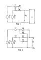
- Sources with the voltage U 1 and U 2 can be connected there in series via switches S11 and S12 or S21 and S22 optionally to input terminals K M of a measuring device (not shown).
- Diverter switches S13 and S23 connect the connection points of the switches in series to zero potential. These discharge switches are controlled so that the connection point of the open series switch is at zero potential. But this is above the voltage source with the output voltage U 2, the series connection of the blocking resistance of the switch S12 with the volume resistance of the closed discharge switch S13.
- the voltage source that is connected in each case is impermissibly stressed by these parallel series connections of a switch blocking resistor and a switch contact resistance.
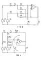
- FIG. 3 shows a circuit which corresponds to the invention.
- the measuring device-side connections of the series switches S12 and S22 connected downstream are connected to one of the inputs of an amplifier V, which is operated as a voltage follower.
- the output connections of the diverter switches S13 and S23 are connected to the output terminal of amplifier V.
- the discharge switch S13 which is assigned to the non-connected voltage source with the voltage U 1 , is closed and the discharge switch S23, which belongs to the connected source with the output voltage U 2 , is open. Because the amplifier V is operated as a voltage follower, the same voltage is present at its output terminal as at its input terminal connected to the source connected.
- the connection point of the two blocked switches S11 and S12 therefore carries the same voltage as the connection of the switch S12 on the output side.
- FIG. 3 The equivalent circuit diagram of the circuit according to FIG. 3 is shown in FIG.
- the blocking or volume resistances of the individual switches are indicated by indices contain the switch designation. Closed switches can be recognized by an additional index D as volume resistance.
- switches S11, S12 and S13 the following applies according to the node rule:
- Equation (1) can be transformed into:
- FIG. 5 shows a circuit which corresponds in principle to the circuit according to FIG. 3. However, it is tailored to the special case in which a disruptive effect only arises when the blocking currents of a certain number of blocked switches of the sources that are not connected are added. A smaller number of sources with first switches can be found here can be combined in parallel into groups and a group can be assigned a second switch in series with it and a diverter switch.
- a source with the output voltage U 1 is connected to an input terminal of the amplifier V via two series switches S11 and S12.
- G U1n is at the connecting point of the series switches S11 and S12 in parallel via a switch S1n a source with the chipboard now connected.
- the index n indicates that several sources can still be connected to the same connection point, up to a number for which the reverse currents via the switches S1n are still below a specified error limit. Sources exceeding this number are combined via switch S2n and switch S21 to form a second group of sources.
- the switch S21 is followed by a series switch S22. At the connection point of the two switches there is a diverter switch S23, which is closed and connects the connection point of the series switches S21 and S22 assigned to sources that are not currently connected to the output terminal of the amplifier V.
Landscapes
- Physics & Mathematics (AREA)
- General Physics & Mathematics (AREA)
- Measurement Of Current Or Voltage (AREA)
Priority Applications (1)
| Application Number | Priority Date | Filing Date | Title |
|---|---|---|---|
| AT83103526T ATE14938T1 (de) | 1982-04-29 | 1983-04-12 | Durchschaltung mehrerer spannungs- oder stromquellen an eine gemeinsame messeinrichtung. |
Applications Claiming Priority (2)
| Application Number | Priority Date | Filing Date | Title |
|---|---|---|---|
| DE3216020A DE3216020C1 (de) | 1982-04-29 | 1982-04-29 | Vorrichtung zur Herstellung der Schaltverbindungen von mehreren Spannungs- oder Stromquellen mit sperrstrombehafteten Schaltern zu einer gemeinsamen Messeinrichtung |
| DE3216020 | 1982-04-29 |
Publications (2)
| Publication Number | Publication Date |
|---|---|
| EP0093285A1 true EP0093285A1 (fr) | 1983-11-09 |
| EP0093285B1 EP0093285B1 (fr) | 1985-08-14 |
Family
ID=6162290
Family Applications (1)
| Application Number | Title | Priority Date | Filing Date |
|---|---|---|---|
| EP83103526A Expired EP0093285B1 (fr) | 1982-04-29 | 1983-04-12 | Interconnexion de plusieurs sources de tension ou de courant avec un dispositif de mesure commun |
Country Status (3)
| Country | Link |
|---|---|
| EP (1) | EP0093285B1 (fr) |
| AT (1) | ATE14938T1 (fr) |
| DE (1) | DE3216020C1 (fr) |
Families Citing this family (2)
| Publication number | Priority date | Publication date | Assignee | Title |
|---|---|---|---|---|
| DE4320818A1 (de) * | 1993-06-23 | 1995-01-05 | Leybold Ag | Meßverstärker |
| DE19515491A1 (de) * | 1995-04-27 | 1996-10-31 | Abb Patent Gmbh | Eingangsschaltung für die Erfassung, Auswertung oder Weiterverarbeitung eines Sensorsignals |
Citations (2)
| Publication number | Priority date | Publication date | Assignee | Title |
|---|---|---|---|---|
| DE2203306B1 (de) * | 1972-01-25 | 1973-08-23 | Siemens Ag | Schaltungsanordnung zur Nullpunktsverschiebung von Messspannungen |
| DE2927264B1 (de) * | 1979-07-05 | 1980-10-02 | Siemens Ag | Schaltungsanordnung mit mindestens einer durchzuschaltenden Versorgungsspannungsquelle |
-
1982
- 1982-04-29 DE DE3216020A patent/DE3216020C1/de not_active Expired
-
1983
- 1983-04-12 EP EP83103526A patent/EP0093285B1/fr not_active Expired
- 1983-04-12 AT AT83103526T patent/ATE14938T1/de not_active IP Right Cessation
Patent Citations (2)
| Publication number | Priority date | Publication date | Assignee | Title |
|---|---|---|---|---|
| DE2203306B1 (de) * | 1972-01-25 | 1973-08-23 | Siemens Ag | Schaltungsanordnung zur Nullpunktsverschiebung von Messspannungen |
| DE2927264B1 (de) * | 1979-07-05 | 1980-10-02 | Siemens Ag | Schaltungsanordnung mit mindestens einer durchzuschaltenden Versorgungsspannungsquelle |
Non-Patent Citations (2)
| Title |
|---|
| IBM TECHNICAL DISCLOSURE BULLETIN, Band 22, Nr. 8B, Januar 1980 A.J. BUTLER et al. "High-speed switchable voltage-controlled current/voltage source", Seiten 3597-3598 * |
| RADIO FERNSEHEN ELEKTRONIK, Band 23, Nr. 19, 1974 W. STEFFEN "Elektronischer Messstellenumschalter mit MOS-Bauelementen", Seiten 640-643 * Seiten 640-643 * * |
Also Published As
| Publication number | Publication date |
|---|---|
| DE3216020C1 (de) | 1983-10-06 |
| EP0093285B1 (fr) | 1985-08-14 |
| ATE14938T1 (de) | 1985-08-15 |
Similar Documents
| Publication | Publication Date | Title |
|---|---|---|
| DE19802604A1 (de) | Motor-Steuergeräteschaltung | |
| DE1289100B (fr) | ||
| DE1762972B2 (de) | Steuerbare spannungsquelle | |
| CH615504A5 (fr) | ||
| DE3019761C2 (de) | Schaltungsanordnung zum Zuführen von Signalen an eine Fernsprechleitung | |
| EP0093285B1 (fr) | Interconnexion de plusieurs sources de tension ou de courant avec un dispositif de mesure commun | |
| DE19838657A1 (de) | Schaltungsanordnung zum Erfassen des Laststromes eines durch Feldeffekt steuerbaren Leistungs-Halbleiterbauelementes | |
| DE2552691C3 (de) | Spannungsprüfschaltung | |
| DE3010267C2 (fr) | ||
| DE1945125A1 (de) | Analog-Multiplikator | |
| DE2329579C3 (de) | Quadrier- oder Effektivwertgleichrichter-Schaltung | |
| DE3109375C2 (fr) | ||
| DE2304211C2 (de) | Leitungsprüfer | |
| DE2419335C2 (de) | Elektronischer negativer Widerstand | |
| DE3806058C2 (fr) | ||
| DE102017115511A1 (de) | Pegelwandler und ein Verfahren zum Wandeln von Pegelwerten in Fahrzeugsteuergeräten | |
| DE4124474C2 (de) | Schaltungsanordnung zur Prüfung einphasiger Elektrizitätszähler mit galvanisch verbundenem Strom- und Spannungspfad | |
| DE624150C (de) | Umschaltbares stromverbrauchendes Messgeraet mit mehreren Spulengruppen | |
| DE2010329A1 (fr) | ||
| DE2049579C3 (fr) | ||
| DE3151082A1 (de) | Schaltungsanordnung zur erweiterung des linearitaetsbereiches eines steuerbaren widerstandes | |
| DE102020209183A1 (de) | Matrixschaltung zur Verarbeitung eines Vektors von Spannungen | |
| DE2329254A1 (de) | Stromwandler mit aktivem lastabschluss | |
| DE2950369C2 (de) | Schaltungsanordnung zur Verschiebung des Ausgangsstrombereich es eines Operationsverstärkers | |
| DE2531475B2 (de) | Schaltungsanordnung mit einer steuerbaren impedanz |
Legal Events
| Date | Code | Title | Description |
|---|---|---|---|
| PUAI | Public reference made under article 153(3) epc to a published international application that has entered the european phase |
Free format text: ORIGINAL CODE: 0009012 |
|
| AK | Designated contracting states |
Designated state(s): AT BE CH FR GB IT LI NL SE |
|
| 17P | Request for examination filed |
Effective date: 19840507 |
|
| ITF | It: translation for a ep patent filed |
Owner name: STUDIO JAUMANN |
|
| GRAA | (expected) grant |
Free format text: ORIGINAL CODE: 0009210 |
|
| AK | Designated contracting states |
Designated state(s): AT BE CH FR GB IT LI NL SE |
|
| REF | Corresponds to: |
Ref document number: 14938 Country of ref document: AT Date of ref document: 19850815 Kind code of ref document: T |
|
| PG25 | Lapsed in a contracting state [announced via postgrant information from national office to epo] |
Ref country code: SE Effective date: 19850830 |
|
| ET | Fr: translation filed | ||
| PLBE | No opposition filed within time limit |
Free format text: ORIGINAL CODE: 0009261 |
|
| STAA | Information on the status of an ep patent application or granted ep patent |
Free format text: STATUS: NO OPPOSITION FILED WITHIN TIME LIMIT |
|
| 26N | No opposition filed | ||
| ITTA | It: last paid annual fee | ||
| PGFP | Annual fee paid to national office [announced via postgrant information from national office to epo] |
Ref country code: CH Payment date: 19910724 Year of fee payment: 9 |
|
| PGFP | Annual fee paid to national office [announced via postgrant information from national office to epo] |
Ref country code: GB Payment date: 19920326 Year of fee payment: 10 |
|
| PGFP | Annual fee paid to national office [announced via postgrant information from national office to epo] |
Ref country code: AT Payment date: 19920327 Year of fee payment: 10 |
|
| PGFP | Annual fee paid to national office [announced via postgrant information from national office to epo] |
Ref country code: FR Payment date: 19920428 Year of fee payment: 10 Ref country code: BE Payment date: 19920428 Year of fee payment: 10 |
|
| PG25 | Lapsed in a contracting state [announced via postgrant information from national office to epo] |
Ref country code: LI Effective date: 19920430 Ref country code: CH Effective date: 19920430 |
|
| PGFP | Annual fee paid to national office [announced via postgrant information from national office to epo] |
Ref country code: NL Payment date: 19920430 Year of fee payment: 10 |
|
| REG | Reference to a national code |
Ref country code: CH Ref legal event code: PL |
|
| PG25 | Lapsed in a contracting state [announced via postgrant information from national office to epo] |
Ref country code: GB Effective date: 19930412 Ref country code: AT Effective date: 19930412 |
|
| PG25 | Lapsed in a contracting state [announced via postgrant information from national office to epo] |
Ref country code: BE Effective date: 19930430 |
|
| BERE | Be: lapsed |
Owner name: SIEMENS A.G. Effective date: 19930430 |
|
| PG25 | Lapsed in a contracting state [announced via postgrant information from national office to epo] |
Ref country code: NL Effective date: 19931101 |
|
| GBPC | Gb: european patent ceased through non-payment of renewal fee |
Effective date: 19930412 |
|
| NLV4 | Nl: lapsed or anulled due to non-payment of the annual fee | ||
| PG25 | Lapsed in a contracting state [announced via postgrant information from national office to epo] |
Ref country code: FR Effective date: 19931229 |
|
| REG | Reference to a national code |
Ref country code: FR Ref legal event code: ST |