EP0091868B1 - Schaltung zur Kontrastverbesserung eines Details in einem Videobild - Google Patents
Schaltung zur Kontrastverbesserung eines Details in einem Videobild Download PDFInfo
- Publication number
- EP0091868B1 EP0091868B1 EP19830400703 EP83400703A EP0091868B1 EP 0091868 B1 EP0091868 B1 EP 0091868B1 EP 19830400703 EP19830400703 EP 19830400703 EP 83400703 A EP83400703 A EP 83400703A EP 0091868 B1 EP0091868 B1 EP 0091868B1
- Authority
- EP
- European Patent Office
- Prior art keywords
- circuit
- window
- video signal
- expanding
- contrast
- Prior art date
- Legal status (The legal status is an assumption and is not a legal conclusion. Google has not performed a legal analysis and makes no representation as to the accuracy of the status listed.)
- Expired
Links
- 230000000295 complement effect Effects 0.000 claims description 5
- 239000003990 capacitor Substances 0.000 description 9
- 238000011144 upstream manufacturing Methods 0.000 description 4
- 230000009471 action Effects 0.000 description 3
- 230000000903 blocking effect Effects 0.000 description 3
- 238000010586 diagram Methods 0.000 description 3
- 230000007704 transition Effects 0.000 description 2
- 238000011282 treatment Methods 0.000 description 2
- 230000003321 amplification Effects 0.000 description 1
- 238000001514 detection method Methods 0.000 description 1
- 238000002955 isolation Methods 0.000 description 1
- 238000003199 nucleic acid amplification method Methods 0.000 description 1
- 238000005457 optimization Methods 0.000 description 1
- 230000010355 oscillation Effects 0.000 description 1
- 230000000737 periodic effect Effects 0.000 description 1
- 230000004044 response Effects 0.000 description 1
- 230000001629 suppression Effects 0.000 description 1
Images


Classifications
-
- H—ELECTRICITY
- H04—ELECTRIC COMMUNICATION TECHNIQUE
- H04N—PICTORIAL COMMUNICATION, e.g. TELEVISION
- H04N5/00—Details of television systems
- H04N5/14—Picture signal circuitry for video frequency region
- H04N5/20—Circuitry for controlling amplitude response
Definitions
- the present invention relates to video signal processing circuits, placed in a television camera or monitor to modify the characteristics of the video signal, and it relates more precisely to circuits tending to modify the contrast of all or part of the image produced. on the screen of a monitor (cf. FR-A-1481969).
- contrast adjustment circuits which compress or expand the amplitude of the video signal to decrease or increase the contrast between the darkest points (lower level of the video signal) and the brightest points (level signal) of the image.
- the contrast is adjusted by manual action on a potentiometer.
- the present invention provides a new processing circuit, establishing an image contrast such that even under the worst conditions, and in particular when the image has a strong backlight, any interesting part of the image, both in the areas dark only in very light areas, can be reproduced with excellent readability.
- the present invention provides a video signal processing circuit comprising an automatic contrast expansion circuit receiving the video signal and having the function of stretching it in amplitude by aligning it between a lower voltage reference. and a higher reference of predetermined voltage, a window generator producing a window signal, a switching circuit controlled by the window generator for directing to the output of the processing circuit, on the one hand, the video signal processed by the circuit expansion during time intervals corresponding to the window and, on the other hand, the video signal during the remaining time intervals of the image, i.e.
- the expansion circuit is also controlled by the window generator to align the darkest point of the window to the lower voltage reference and to the upper voltage reference the brightest point of the window, and that it includes an additional automatic contrast expansion circuit receiving said video signal, having the same function as the first but relatively to the entire image, said switching circuit to said output of the processing circuit the video signal processed by said complementary circuit during said time intervals outside the window.
- this image undergoes contrast optimization independent of the contrast of the rest of the image, that is to say that if this portion of image is a dark area of a backlit image, this area will appear on the screen with maximum contrast ranging from white to black.
- the voltage references of the two expansion circuits may or may not be the same; in particular they can be individually adjusted by potentiometers.
- the window is preferably adjustable both in width as in height and in position: in a fire control system, it can be controlled by the position and the size of a pointing reticle visible on the screen and produced by superimposing slots of selected width, position and luminance in the video signal.
- the invention makes it possible in particular to avoid that the observer interested in a poorly contrasted image portion is obliged to adjust manually the contrast as a function of this portion: on the one hand he would have to constantly modify this setting, and on the other hand the contrast outside the interesting portion would be very bad. This last drawback would also be preserved if manual adjustment were replaced by an automatic contrast expansion made as a function of the signal level inside a window delimiting the interesting image portion.
- Figure 1 shows a video signal in the form of successive signal portions each corresponding to a line, separated from each other by line feed intervals. Only three successive lines have been represented, but if one examines the signal over an entire image, that is to say for example over an entire frame of 625 lines, one can locate a minimum signal level Vmin and a level maximum signal Vmax.
- this signal would generate an image whose brightness varies between a light gray level corresponding to Vmax and a level of darker gray corresponding to Vmin.
- An automatic contrast expansion circuit will have the function of stretching the signal in height so that the level Vmin becomes equal to a lower voltage reference V1 and the level Vmax becomes equal to a higher voltage reference V2, where V2 corresponds to “white” (maximum brightness) and V1 to “black” (minimum brightness). V1 and V2 can be manually adjusted to define what is called white and black, but, once this adjustment has been made, the video signal will automatically adjust so as to occupy the entire range of brightnesses intermediate between these two levels.
- This stretching can be broken down into two actions: the first consists (fig. 1 b) of globally shifting the level of the video signal to bring Vmin to V1 (or Vmax to V2); the second consists (fig. 1 c) in amplifying the video signal as a whole so as to bring Vmax to V2 (or Vmin to V1), without modifying the level of Vmin (or Vmax).
- These two actions are in reality simultaneous and are carried out moreover with a certain time constant, that is to say that the Vmin and Vmax levels of the signal are located on at least one complete frame, and this is on the video signal of the following frames that the desired offset and amplification are carried out.
- Fig. 2 shows a high-contrast video signal: in the first part of each line, the signal corresponds to a dark area with little contrast, and in the second part it corresponds to a bright area, also with little contrast.
- the levels Vmin and Vmax of the signal can be brought to V1 and V2 as explained above, but this will increase very little the contrast of a zone Z which interests the operator but whose details are unfortunately not very visible because the video signal in this zone is not very modulated (compared to the global modulation of the signal in the whole image). For example, the signal oscillates in the zone Z between two levels close to V'min and V'max.
- Fig. 3 shows how the processing circuit according to the invention will transform the video signal of FIG. 2: outside the interesting zone Z, represented by a window F extending over a duration T at each line, always in the same place relative to the start of the line, and this on a certain number of lines, always the same with each frame, the video signal undergoes an expansion of contrast as explained in figs. 1 a to 1 c; the minimum level on at least one frame is identified (Vmin) and brought to V1; the maximum level (Vmax) is brought to V2.
- V'min the minimum level of the signal on a frame, considering only the part of the signal included in the window corresponding to the zone Z, is marked (V'min), as well as the maximum level (V'max).
- V'min is brought to V1 and V'max to V2; it may also be reference voltages V1 and V'2 different from V1 and V2 and each adjustable independently of V1 and V2.
- the image in zone Z thus becomes highly contrasted as shown by the large amplitude oscillations of the video signal in zone Z after processing (fig. 3), and this without altering the normal contrast of the rest of the image.
- Fig. 4 shows the image that this can give on a display screen: the zone Z corresponding to a certain number of scanning lines and a certain length of line appears clear and well contrasted on a generally dark background due to the backlight. If the Z zone was taken in a very clear and little contrasted part of the image, it would on the contrary appear overall darker and well contrasted.
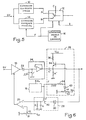
- Fig. 5 shows the block diagram of the processing circuit according to the invention: the video signal SV, not processed or having undergone certain prior treatments, including contrast enhancement treatments such as a contour correction or a gamma correction, is brought to the input of a first automatic contrast expansion circuit 10 acting on the entire image, a circuit the output of which is connected to a first input A of a switching circuit 12.
- contrast enhancement treatments such as a contour correction or a gamma correction
- the signal SV is brought to the input of a second automatic expansion circuit of contrast 14 whose output is connected to another input terminal B of the switching circuit 12.
- the second circuit acts only on a small part of the video signal, delimited by the window F.
- a window generator 16 (slots of duration T for N lines) is therefore provided to control the second circuit 14. This generator also controls the switching circuit 12 to direct to the output of the latter either the signal present on its first input A (outside the window) or the signal present on its second input B (during the window ).
- the input of the second circuit 14 can receive not the video signal SV but a video signal which has undergone processing in the first expansion circuit 10.
- a contour correction and / or gamma correction circuit can be placed upstream or downstream of the entire circuit of FIG. 5; such circuits can also be placed upstream or downstream of the second circuit 14 exclusively, or alternatively a contour correction circuit upstream or downstream of the second circuit exclusively and a gamma correction circuit upstream or downstream of the first circuit .
- the video signal SV which enters the processing circuit may or may not be provided with signal suppression zones, synchronization signals, particular encrusted signals which are superimposed on the image (such as '' a crosshair, or alphanumeric indications or other symbols).
- inlay circuits can be provided downstream of one or other of the contrast expansion circuits 10 and 14 or downstream of the switching circuit 12, the best solution being without doubt to perform these incrustations at the level of the switching circuit 12 which will then have inputs corresponding to the signals to be superimposed (symbolically represented by an input C), and superimposition control inputs (symbolically represented by an input l).
- Symbol generators will be connected to the inputs of signals to be superimposed, while an overlay control circuit (which may include in practice the window generator F) will control at selected times the routing of a particular signal to the output. of the switching circuit 12.
- This circuit includes a variable gain amplifier 18 receiving the video signal to be processed (SV). The gain is controlled by the output of a differential amplifier 20.
- variable gain amplifier 18 The output of the variable gain amplifier 18 is brought, via a connection capacitor 22 and a level blocking circuit (“clamping”) 24, to an alignment circuit at the level lower V1, shown in a dotted frame, designated by 26.
- level blocking circuit 24 The function of circuit 24 is to reduce the video signal blocking level to zero during line feeds.
- the output of the alignment circuit 26, which also constitutes the output of the contrast expansion circuit of FIG. 6 is looped back to an amplifier gain control input 18 via a video signal peak detector represented in a dotted frame 28 and via the differential amplifier 20, an input of which is connected to the peak detector and the other input to the cursor of a potentiometer 21 defining the upper reference voltage V2 (adjustable).
- the peak detector 28 and the alignment circuit 26 receive the signal defining the window F so as to perform a peak detection or level alignment job only during the slots constituting this window.
- the window generator 16, shown in FIG. 6, can moreover establish other periodic signals than the window, such as for example a line synchronization signal SL for actuating during the line return moments the level blocking device 24 (shown in the form of a switch zero setting) controlled by the SL signal and a follower amplifier with high input impedance.
- the peak detector is for example simply constituted by a rectifying diode 30 in series with a switch 32 closed only during the slots of the window F, and with a set of a resistor R and a capacitor C in parallel.
- the capacitor charges on the video signal peaks and discharges with an RC time constant corresponding to approximately one scan frame.
- the level of charge of the capacitor C is applied to the differential amplifier 20 which compares this level to V2 and acts on the gain of the amplifier 18 so that in the next frame the video signal is amplified or reduced in a tending direction to bring the charge level of the capacity closer to V2.
- the circuit 26 for lower level alignment of the video signal is constituted as follows: a capacitor C 'receives on a frame the signal to be aligned and is connected by the other frame to a resistor R' which is the resistor emitter of a transistor 34 further polarized by a collector resistor 36 connected to a voltage Vcc.
- the base of the transistor is also connected by a diode 40 to the cursor of a potentiometer 42 defining the lower voltage reference value V1.
- the base of the transistor is connected by a resistor 44 to the output of the window generator 16.
- the output of the alignment circuit 26, which is the output of the contrast expansion circuit, is taken from the emitter of the transistor 34 (connected to the capacitor C 'and to the resistor R').
- the transistor 34 is blocked and the video signal is transmitted as is from the input to the output of the alignment circuit 26.
- the transistor can conduct, but only if the video signal is lower than the reference V1, and, in the latter case, the conduction of the transistor causes a charge of the capacitor C '.
- the capacitor takes an average charge value such that the signal present on the emitter of the transistor is always just greater than V1.
- the circuit 26 therefore performs the alignment on V1 of the minimum voltage of the portion of the video signal included in the window F.
- the circuit of fig. 6 constitutes the circuit 14 of FIG. 5. It can also constitute the expansion circuit 10 over the entire image, provided that the circuit 26 and the circuit 28 are controlled not by the slots of window F but by slots of a window F 'which corresponds to the entire image.
- This command through the window F ' is obviously necessary so that the line feed or frame return periods of the video signal are not taken into account for the expansion of the image because the level of video signal during these returns is independent of the image to observe.
- the same generator 16 can be used to generate the window F, the window F ′, the synchronization signals SL and other useful signals if necessary.
- the window generator 16 can be controlled by a microprocessor which also controls generators of symbols, reticles, etc., with a view to embedding appropriate signals in the video signal at the switching circuit 12 of FIG. 5 outside the window or during the window.
- this microprocessor will have the task of defining the possibly variable characteristics of the window: width, height, position, in particular if these characteristics are directly linked to the corresponding characteristics of a pointing reticle which itself depends on external data (supplied to the microprocessor) such as in particular the distance from a target.
- the switching circuit 12 is, in turn, a simple switching circuit comprising analog gates which allow the signal applied to one or other of its inputs to pass to the output of the circuit, as a function of appropriate control slots.
- the invention has been described by taking as an example the processing of a video signal corresponding to line-by-line scanning (television type), but it is understood that it should not be limited to this type of scanning.
Landscapes
- Engineering & Computer Science (AREA)
- Multimedia (AREA)
- Signal Processing (AREA)
- Television Receiver Circuits (AREA)
- Controls And Circuits For Display Device (AREA)
- Picture Signal Circuits (AREA)
Claims (7)
Applications Claiming Priority (2)
| Application Number | Priority Date | Filing Date | Title |
|---|---|---|---|
| FR8206270 | 1982-04-09 | ||
| FR8206270A FR2525058B1 (fr) | 1982-04-09 | 1982-04-09 | Circuit d'amelioration du contraste d'un detail d'une image video |
Publications (2)
| Publication Number | Publication Date |
|---|---|
| EP0091868A1 EP0091868A1 (de) | 1983-10-19 |
| EP0091868B1 true EP0091868B1 (de) | 1985-12-18 |
Family
ID=9272956
Family Applications (1)
| Application Number | Title | Priority Date | Filing Date |
|---|---|---|---|
| EP19830400703 Expired EP0091868B1 (de) | 1982-04-09 | 1983-04-06 | Schaltung zur Kontrastverbesserung eines Details in einem Videobild |
Country Status (3)
| Country | Link |
|---|---|
| EP (1) | EP0091868B1 (de) |
| DE (1) | DE3361534D1 (de) |
| FR (1) | FR2525058B1 (de) |
Families Citing this family (9)
| Publication number | Priority date | Publication date | Assignee | Title |
|---|---|---|---|---|
| FR2583243B1 (fr) * | 1985-06-07 | 1987-11-20 | Thomson Csf | Circuit d'amelioration du contraste d'une image video |
| NL8502564A (nl) * | 1985-09-19 | 1987-04-16 | Philips Nv | Beeldsignaalverwerkingsschakeling. |
| FR2604841B1 (fr) * | 1986-10-07 | 1988-11-25 | Etude Signal | Dispositif de transformation d'un signal par stabilisation et rehaussement de la dynamique dudit signal |
| JPH0383460A (ja) * | 1989-08-28 | 1991-04-09 | Matsushita Electric Ind Co Ltd | 画像ズーム装置 |
| GB9201837D0 (en) * | 1992-01-27 | 1992-03-11 | Philips Electronic Associated | Television receiver |
| DE4239365A1 (de) * | 1992-11-24 | 1994-05-26 | Philips Patentverwaltung | Schaltungsanordnung zum Verarbeiten eines Videosignals |
| FR2751156B1 (fr) * | 1996-07-11 | 1998-10-09 | Christophel Claude | Procede de traitement d'un signal video |
| US6005636A (en) * | 1997-03-27 | 1999-12-21 | Sharp Laboratories Of America, Inc. | System for setting user-adjustable image processing parameters in a video system |
| CN102955277B (zh) * | 2012-11-07 | 2014-11-19 | 北京三五九投资有限公司 | 一种增强pdlc显示器对比度的方法 |
Family Cites Families (3)
| Publication number | Priority date | Publication date | Assignee | Title |
|---|---|---|---|---|
| DE1241869B (de) * | 1962-05-12 | 1967-06-08 | Fernseh Gmbh | Schaltungsanordnung zur Verbesserung der Detailerkennbarkeit eines Fernsehbildes |
| FR1481969A (fr) * | 1966-01-14 | 1967-05-26 | Dispositif pour l'augmentation des contrastes d'une image de télévision | |
| FR2406922A1 (fr) * | 1977-10-21 | 1979-05-18 | Thomson Csf | Dispositif d'expansion de contraste video et systeme comportant un tel dispositif |
-
1982
- 1982-04-09 FR FR8206270A patent/FR2525058B1/fr not_active Expired
-
1983
- 1983-04-06 DE DE8383400703T patent/DE3361534D1/de not_active Expired
- 1983-04-06 EP EP19830400703 patent/EP0091868B1/de not_active Expired
Also Published As
| Publication number | Publication date |
|---|---|
| EP0091868A1 (de) | 1983-10-19 |
| DE3361534D1 (en) | 1986-01-30 |
| FR2525058A1 (fr) | 1983-10-14 |
| FR2525058B1 (fr) | 1986-06-06 |
Similar Documents
| Publication | Publication Date | Title |
|---|---|---|
| US4994918A (en) | Method and circuit for the automatic correction of errors in image steadiness during film scanning | |
| WO1991012690A1 (fr) | Dispositif d'augmentation de dynamique d'une camera | |
| EP0091868A1 (de) | Schaltung zur Kontrastverbesserung eines Details in einem Videobild | |
| FR2628280A1 (fr) | Appareil de traitement adaptif pour l'etalement d'un signal video | |
| WO1994021080A1 (fr) | Dispositif d'affichage de caracteres dans un systeme video | |
| EP0127451B1 (de) | Automatisches Fokussierungssteuersystem für eine Videokamera | |
| US4279003A (en) | Picture contrast-increasing arrangements | |
| NL192762C (nl) | Schakeling voor zwartniveauherstel van het beeldsignaal in een televisie-ontvanger. | |
| FR2470502A1 (fr) | Circuit de traitement d'un signal video notamment pour un recepteur de television | |
| JPS5880970A (ja) | コントラスト増大改良方法 | |
| DE69930591T2 (de) | Bildaufnahme- und Bildwiedergabegerät | |
| FR2508265A1 (fr) | Circuit de desaccentuation video | |
| FR2587863A1 (fr) | Recepteur de television avec signaux selectionnables d'entree video | |
| FR2473240A1 (fr) | Camera couleur comportant un circuit de correction d'ouverture verticale | |
| JPH0276481A (ja) | 撮像装置 | |
| US6529243B1 (en) | Method for electronic reduction of the contrast of video images as early as during recording | |
| FR2530395A1 (fr) | Etage d'attaque a gain pouvant etre preetabli a la main pour un tube-image dans un systeme de reglage automatique de la polarisation du tube-image | |
| FR2629658A1 (fr) | Circuit d'amelioration du contraste d'une image video, notamment d'une partie de l'image | |
| US3600511A (en) | Apparatus for controlling the operating potential of a vidicon | |
| EP0205383B1 (de) | Schaltungsanordnung zur Verbesserung des Kontrastes eines Videobildes | |
| FR2490047A1 (fr) | Circuit et procede de reglage automatique du courant de faisceau d'un tube analyseur de camera video | |
| US20050001925A1 (en) | Exposure control device | |
| JPH09247552A (ja) | 固体撮像装置の信号処理回路 | |
| EP0649248B1 (de) | Bildanzeigevorrichtung mit Modulation der Lichtpunktgeschwindigkeit | |
| EP0135414A1 (de) | Optoelektronischer Sensor für Bildaufnahme |
Legal Events
| Date | Code | Title | Description |
|---|---|---|---|
| PUAI | Public reference made under article 153(3) epc to a published international application that has entered the european phase |
Free format text: ORIGINAL CODE: 0009012 |
|
| AK | Designated contracting states |
Designated state(s): DE GB IT NL |
|
| 17P | Request for examination filed |
Effective date: 19840216 |
|
| RBV | Designated contracting states (corrected) |
Designated state(s): DE GB |
|
| GRAA | (expected) grant |
Free format text: ORIGINAL CODE: 0009210 |
|
| AK | Designated contracting states |
Designated state(s): DE GB |
|
| REF | Corresponds to: |
Ref document number: 3361534 Country of ref document: DE Date of ref document: 19860130 |
|
| PLBE | No opposition filed within time limit |
Free format text: ORIGINAL CODE: 0009261 |
|
| STAA | Information on the status of an ep patent application or granted ep patent |
Free format text: STATUS: NO OPPOSITION FILED WITHIN TIME LIMIT |
|
| 26N | No opposition filed | ||
| PGFP | Annual fee paid to national office [announced via postgrant information from national office to epo] |
Ref country code: DE Payment date: 19890316 Year of fee payment: 7 |
|
| PGFP | Annual fee paid to national office [announced via postgrant information from national office to epo] |
Ref country code: GB Payment date: 19890331 Year of fee payment: 7 |
|
| PG25 | Lapsed in a contracting state [announced via postgrant information from national office to epo] |
Ref country code: GB Effective date: 19900406 |
|
| GBPC | Gb: european patent ceased through non-payment of renewal fee | ||
| PG25 | Lapsed in a contracting state [announced via postgrant information from national office to epo] |
Ref country code: DE Effective date: 19910101 |