EP0088568B1 - Anzeigevektorgenerator mit Verwendung einer Sinus/Cosinus-Aufspeicherung - Google Patents
Anzeigevektorgenerator mit Verwendung einer Sinus/Cosinus-Aufspeicherung Download PDFInfo
- Publication number
- EP0088568B1 EP0088568B1 EP83301040A EP83301040A EP0088568B1 EP 0088568 B1 EP0088568 B1 EP 0088568B1 EP 83301040 A EP83301040 A EP 83301040A EP 83301040 A EP83301040 A EP 83301040A EP 0088568 B1 EP0088568 B1 EP 0088568B1
- Authority
- EP
- European Patent Office
- Prior art keywords
- digital
- deflection
- accumulator
- signals
- signal
- Prior art date
- Legal status (The legal status is an assumption and is not a legal conclusion. Google has not performed a legal analysis and makes no representation as to the accuracy of the status listed.)
- Expired
Links
Images

Classifications
-
- G—PHYSICS
- G09—EDUCATION; CRYPTOGRAPHY; DISPLAY; ADVERTISING; SEALS
- G09G—ARRANGEMENTS OR CIRCUITS FOR CONTROL OF INDICATING DEVICES USING STATIC MEANS TO PRESENT VARIABLE INFORMATION
- G09G1/00—Control arrangements or circuits, of interest only in connection with cathode-ray tube indicators; General aspects or details, e.g. selection emphasis on particular characters, dashed line or dotted line generation; Preprocessing of data
- G09G1/06—Control arrangements or circuits, of interest only in connection with cathode-ray tube indicators; General aspects or details, e.g. selection emphasis on particular characters, dashed line or dotted line generation; Preprocessing of data using single beam tubes, e.g. three-dimensional or perspective representation, rotation or translation of display pattern, hidden lines, shadows
- G09G1/08—Control arrangements or circuits, of interest only in connection with cathode-ray tube indicators; General aspects or details, e.g. selection emphasis on particular characters, dashed line or dotted line generation; Preprocessing of data using single beam tubes, e.g. three-dimensional or perspective representation, rotation or translation of display pattern, hidden lines, shadows the beam directly tracing characters, the information to be displayed controlling the deflection and the intensity as a function of time in two spatial co-ordinates, e.g. according to a cartesian co-ordinate system
- G09G1/10—Control arrangements or circuits, of interest only in connection with cathode-ray tube indicators; General aspects or details, e.g. selection emphasis on particular characters, dashed line or dotted line generation; Preprocessing of data using single beam tubes, e.g. three-dimensional or perspective representation, rotation or translation of display pattern, hidden lines, shadows the beam directly tracing characters, the information to be displayed controlling the deflection and the intensity as a function of time in two spatial co-ordinates, e.g. according to a cartesian co-ordinate system the deflection signals being produced by essentially digital means, e.g. incrementally
Definitions
- the present invention relates to stroke writing cathode ray tube (CRT) displays and are particularly to vector generators therefor.
- a variety of vector generator arrangements for stroke writing displays are known in the prior art. With such displays, images are formed by a composite of individually drawn vectors with concatenated vectors being utilised to compose display shapes and symbology. For present day applications, it is often desirable to display rotation of the images.
- a further desideratum of present day vector generators is precise control of vector writing speed, whereby writing speeds may be fast enough for compatibility with present day processing rates and furthermore, whereby smooth vectors may be written at a controlled slow speed.
- Slow vectors may be desirable to enhance display brightness without utilising the contentional CRT brightness electronics. This is desirable since adjustment of the CRT brightness control often has a defocussing effect.
- the vector speed control may be utilised to adjust brightness on both shadow mask and penetration phosphor colour CRTs as well as on other types of CRTs.
- Analogue vector generators utilising analogue ramp generators are known in the art. Such analogue vector generators utilise an X ramp generator and a Y ramp generator to provide CRT deflection signals for generating the vectors. An X multiplier and a Y multiplier are utilised to rotate the images which results in a loss of precision. Such analogue vector generators are generally incompatible with current digitally oriented systems and are imprecise, bulky and require significant amounts of power. The operating characteristics of the prior art analogue vector generators drift with time and temperature, thereby distorting the displayed images due to aging of the components.
- Digital stroke vector generators are also known in the prior art.
- One type of digital vector generator prevalent in the art utilises X and Y binary rate multipliers in the X and Y deflection axes, respectively.
- the parallel digital multiplier inputs to the binary rate multipliers comprise the sine and cosine, respectively, of the angle of the vector to be drawn.
- the system clock signal applied to each of the binary rate multipliers is multiplied by the sine and cosine, thereby providing X and Y clock pulse trains having pulse rates proportional to the sine and cosine.
- the X and Y clock pulses are counted in respective binary counters, the outputs of which provide digital X and Y position signals to respective X and Y digital-to-analogue converters (DACs).
- DACs digital-to-analogue converters
- DACs that are conventionally utilised in digital vector generators typically are twelve bits wide. Accordingly, in a rate multiplier vector generator utilising twelve bit DACs, the sine and cosine rate inputs, the rate multipliers and the counters are also twelve bits wide. Thus, present day DACs providing twelve bit resolution can resolve to one part in 4,096. Such DACs have a settling time when changing from one value to another of approximately 300 nanoseconds. Therefore, when operating at maximum capability, the vector generator can traverse the full scale of the DAC range in approximately 1200 microseconds. Under such an arrangement, the input clock to the rate multipliers is 3.3 megahertz. This vector speed is an order of magnitude slower than typically required for CRT displays.
- Rate multiplier vector generators may additionally. increase speed by utilising a higher frequency clock input to the rate multipliers. Present day rate multipliers will accept frequencies up to thirteen megahertz. With such a clock input, the speed may be increased by a factor of 4 and if one bit is omitted from the DACs, an eight fold increase in speed can be achieved. It will be appreciated in such an arrangement that because of the limited settling time of the DACs, the DACs are updated at a rate of approximately 3.3 megahertz.
- the rate multiplier vector generator does not provide the resolution in X and Y deflection or the vector velocity control that is required in high performance CRT displays. Because of the inherent operation of rate multipliers, the beam does not move continuously in the X and Y directions and in factthe vector stops for a portion of time generally equal to (1 - X rate) x (1 - Y rate). This effect results in vectors having a granular appearance and the effect is exacerbated for low velocity vectors. With a rate multiplier vector generator, the velocity is reduced by reducing the sine and cosine rate inputs to the multipliers. This increases the proportion of clock cycles at which the rate multipliers do not produce any clockoutput. Thus, the velocity control is achieved by stopping the beam deflection more often and for longer durations for low velocity vectors. Instead, therefore, of generating a smooth slow vector, bright dots along the desired path result.
- rate multipliers cannot be improved further beyond that described above because the required frequency of the clock driving the rate multipliers would necessarily be higher than that accepted by present day rate multipliers.
- errors of the individual vectors will accumulate to degree the quality of the image.
- Increasing the length of the counters would not alleviate the problem since the rate multipliers cannot be driven fast enough to provide the required resolution.
- Displayed vectors are rotated by recomputing the sequence of sines and cosines for the incremental rotations of the vectors.
- the rate multiplier vector generator as described above, the truncation errors of the arithmetic utilised in generating the sine and cosine values accumulate, resulting in distortions of the rotating image.
- a further prior art vector generator is disclosed in U.S. Patent Specification No. 4,115,863 and this generates vectors by applying clock pulses to an up/down counter which through a DAC provides the deflection voltage for one of the display X or Y axes.
- the clock pulses are applied through a gate to a second up/down counter which through a second DAC provides the deflection voltage for the other of the X and Y axes.
- the gate is controlled by the overflow of an accumulator that is repetitively accumulating, under control of the clock pulses, a signal representative of the desired slope of the vector.
- the DAC utilised in the display axis associated with the gated clock derives its input from both the associated up/down counter and the output of the associated accumulator for display resolution enhancement.
- U.S. Patent Specification No. 4,228,510 discloses character generator apparatus for a display having X and Y display axes and respective X and Y deflection means therefor, the deflection means being responsive to digital X and Y deflection signals, respectively, each comprising a predetermined number of bits, the apparatus further comprising a source of digital X rate signal, a source of digital Y rate signal, one of the X and Y rate signals being representative of the sine of the angle of a vector to be generated and the other of the rate signals being representative of the cosine of that angle, and X and Y accumulator means providing respective digital output signals and being responsive from, respectively, to the X and Y rate signals for accumulation thereof. With such an arrangement, one must either accept brightness disparity between vectors at different orientations or employ additional apparatus to overcome this problem.
- vector generator apparatus for a display vector generator apparatus for a display having X and Y display axes and respective X and Y deflection means therefor, the deflection means being responsive to digital X and Y deflection signals, respectively, each comprising a predetermined number of bits
- the apparatus comprising a source of a digital X rate signal, a source of a digital Y rate signal, one of the X and Y rate signals being representative of the sine of the angle of a vector to be generated and the other of the rate signals being representative of the cosine of that angle
- X accumulator means providing a digital output signal and being responsive to the X rate signal for accumulation thereof
- Y accumulator means providing a digital output signal and being responsive to the Y rate signal for accumulation thereof, characterised in that the digital output signal of the X accumulator means has a greater number of bits than said predetermined number, the most significant bits thereof providing the digital X deflection signal, the digital X rate signal comprising fewer bits
- the present invention overcomes all of the above described disadvantages of the prior art by providing a vector generator comprising a digital accumulator for each of the X and Y axes of the display.
- the X and Y accumulators provide digital position signals to respective X and Y DACs, having outputs which provide the respective X and Y deflection signals to the display.
- the accumulators are wider than the respective DACs with the most significant bits of the accumulator providing the inputs to the DACs.
- Digital X and Y rate signals proportional to the sine and cosine of the vector angle are accumulated in the X and Y accumulators.
- the X and Y rate signals are combined with the contents of the accumulators at the least significant portions thereof.
- an accumulator for implementing in the present invention is illustrated. Two such accumulators are utilised in the invention; one for the X deflection axis and one for the Y deflection axis. In the preferred embodiment of the invention, the Y accumulator processes the vector sine and the X accumulator processes the vector cosine.
- the accumulator of Figure 1 comprises a twenty-four bit adder 10 configured in the preferred embodiment to perform two's complement arithmetic.
- the A input of the adder 10 is provided by a twenty-four bit bus 11 which accepts the rate signal to be accumulated.
- the X rate signal is proportional to the cosine of the vector angle
- the Y rate signal is proportional to the sine of the vector angle.
- the sine and cosine inputs to the respective accumulators are sixteen bit two's complement digital signals with the eight most significant bits thereof sign extended.
- the digital rate signal on the bus 11 is provided throughout the vector writing time and may be positive or negative with a value that controls beam deflection per clock cycle of between 0 and 1/256 of full screen range.
- the twenty-four bit output of the adder 10 is provided on a bus 12 as an input to a twenty-four bit multiplexer 13.
- the vector initial position (X or Y) is provided on a twenty-four bit bus 14 as a second input to the multiplexer 13.
- the bus 14 provides a sixteen bit initial position to the multiplexer 13 with the eight least significant bits of the twenty-four bit word being zeroes.
- a multiplexer control signal is provided on a lead 15 to the multiplexer 13.
- the multiplexer control signal on the lead 15 controls the multiplexer 13 to connect either the bus 12 or the bus 14 to the multiplexer output bus 16.
- the initial position bus 14 is connected to the multiplexer output bus 16 during the initial position load phase of the vector generator, whereas the adder output bus 12 is connected to the bus 16 during the vector writing phase thereof.
- the twenty-four bit output bus 16 from the multiplexer 13 is coupled as an input to a twenty-four bit latch 17.
- the twenty-four bit output from the latch 17 on a twenty four bit bus 18 is applied as the B input to the adder 10.
- the latch 17 also receives a master clock signal on a lead 19 which strobes the twenty-four bit input on the bus 16 into the latch 17.
- the adder 10 combines the twenty-four bit accumulated value on the bus 18 with the twenty-four bit rate on the bus 11, which sum is strobed into the latch 17 during each clock pulse on the lead 19. Therefore, for each clock pulse on the lead 19, the sum of the rate signal on the bus 11 with the accumulated value in the latch 17 is strobed into the latch 17.
- the value in the latch 17 increases or decreases linearly. Since two's complement quantities and arithmetic are utilised, the sign of the rate signal on the bus 11 controls whether value in the latch 17 will be incremented or decremented by the rate signal.
- the clock frequency on the lead 19 is selected to be as fast as the deflection DACs can convert the digital values from the latch 17 into analogue equivalents. In other words, the frequency of the clock is selected to be as high as the settling time of the DACs will permit.
- the twenty-four bit accumulated value on the bus 18 is utilised as follows.
- the most significant bit is an out-of-bounds signal that blanks the CRT video and staticises the digital deflection signals to prevent the screen image from exhibiting the wrap-around phenomenon where, for example, a symbol moves off screen at the top and appears at the bottom. Further details of utilising the out-of-bounds bit will be provided hereinbelow.
- the next twelve most significant bits of the bus 18 provide the deflection signal to the DAC utilising the full range of commercially procurable twelve- bit DACs.
- the remaining eleven bits of the bus 18 enhance long term accuracy by reducing buildup errors that occur over the span of many vectors when a group of vectors is rotated or otherwise transformed in, for example, a change of perspective.
- the master clock is stopped and the sixteen bit initial position on the bus 14 is loaded into the latch 17 through the multiplexer 13.
- Vector writing is initiated by starting the master clock on the lead 19.
- the length of the vector is controlled by the number of clock pulses provided to the latch 17.
- the rate signal on the bus 11 is added to the previous value in the latch 17 and the sum is inserted into the latch 17. In this manner, the value in the latch 17 increases or decreases linearly, thereby providing the deflection voltages for writing the vector.
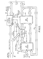
- a sixteen bit adder 30 receives the sixteen bit rate signal on a bus 31 at the A input thereof. Similar to that described above, the adder 30 is implemented to perform two's complement arithmetic with the rate signal on the bus 31 being in two's complement format. The most significant bit of the rate signal on the bus 31 is provided on a separate lead 32. The overflow from the adder 30 is provided on a lead 33.
- the rate MSB signal on the lead 32 is binary ZERO. Conversely, when the rate is negative, the rate MSB signal on the lead 32 is binary ONE. Because of the two's complement format utilised, when the rate is positive, the adder 30 will add the rate to the value applied to be B input of the adder and when the rate is negative, the rate will be sub -tracted from the value applied atthe B inputto the adder.
- the signals on the leads 32 and 33 are utilised to control the up/down counter that implements the eight most significant bits of the twenty-four bit accumulator in a manner to be described.
- the most significant byte from the adder 30 is applied as an input to an eight bit initial position multiplexer 34 via an eight bit bus 35.
- the sixteen bit initial vector position (X or Y) is applied to a bus 36, the least significant byte thereof being applied as a second input to the multiplexer 34.
- a multiplexer control signal on a lead 37 controls the multiplexer 34 to connect either the least significant byte of the initial position signal or the most significant byte from the adder 30 to an eight bit multiplexer output bus 38.
- the eight bit output from the multiplexer 34 on the bus 38 and the least significant byte from the adder 30 provide a sixteen bit input to a sixteen bit latch 39.
- the sixteen bit output from the latch 39 is applied via a bus 40 as the B input to the adder 30.
- a mast clock signal on a lead 41 strobes the latch 39, thereby entering the sixteen bit data from the multiplexer 34 and the adder 30.
- the mast clock signal on the lead 41 is of a frequency commensurate with the settling time of the DACs.
- the least significant sixteen bits of the twenty-four bit accumulator of Figure 2 are implemented utilising the sixteen bit adder 30, the eight bit multiplexer 34 and the sixteen bit latch 39.
- the eight most significant bits of the accumulator are implemented by an eight bit up/down counter 42.
- the counter 42 is set to its initial position (X or Y) by the most significant byte of the initial position signal on the bus 36.
- the clock input to the counter 42 is provided by the master clock signal on the lead 41 and the up/down control for the counter is provided by the rate most significant bit on the lead 32.
- Carry out logic implemented in the present embodiment by an exclusive OR gate 43 has an output connected to the enable input of the counter 42.
- the inputs to the exclusive OR gate 43 are provided by the rate most significant bit on the lead 32 and the adder overflow signal on the lead 33. Because of the two's complement configuration of the adder 30 and the two's complement format of the initial position signal and the rate signal, the counter 42 is controlled to count upwardly when the rate signal on the bus 31 is positive and downwardly when the rate signal is negative.
- the exclusive OR gate 43 enables the counter 42 only when the rate signal is positive and there is an overflow on the lead 33 or when the rate signal is negative and there is no carry on the lead 33. For all other conditions, the counter 42 is disabled. Thus, it will be appreciated that the counter 42 functions as an accumulator permitted to change count from one clock pulse to the next by +1, -1 or 0.
- the adder 30 and the latch 39 comprise a sixteen bit parallel accumulator for accumulating the rate signal on the bus 31.
- the counter 42 constitutes an eight bit accumulator for accumulating the carries from the sixteen bit accumulator. It is advantageous to utilise the up/down counter42 as an accumulator because of the simplicity thereof compared with a conventional accumulator. The disadvantage of this arrangement is that the vector speed is limited to 1/128th of the full screen range per clock cycle. This speed is sufficient for practical applications of the invention.
- the most significant bit from the counter 42 is provided on a lead 44 and is utilised as the out-of-bounds bit described above with respect to Figure 1.
- the seven least significant bits of the counter 42 are provided on a bus 45 as the seven most significant input bits to the DAC.
- the five least significant bits of the DAC are provided on a bus 46 from the five most significant bits of the latch 39.
- the accumulator of Figure 2 provides a digital position signal utilising all twelve of the DAC bits.
- the eleven least significant bits of the latch 39 are not provided as an output to the DAC but are utilised in the manner described above with respect to Figure 1 to enhance vector writing precision.
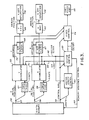
- the vector generator includes a Y-accumulator 50 and an X-accumulator 51 which may be implemented utilising either the accumulator of Figure 1 or the accumulator of Figure 2 or an equivalent thereof.
- the accumulator of Figure 2 is utilised in implementing the preferred embodiment of the invention and Figure 3 will be accordingly described.
- the vector generator includes a digital memory 52 for providing the sixteen-bit X and Y initial position signals, the sixteen-bit X and Y rate signals (cosine and sine) aswell as a length control signal.
- the memory 52 also provides numerous conventional control signals for controlling the loading and writing sequences of the display.
- the memory 52 is part of a conventional microprocessor system for generating and providing the sequences of instructions which specify the vectors to be drawn.
- the vector generator of Figure 3 also includes vector control circuitry represented schematically at 53 and video control circuitry represented schematically at 54.
- the digital memory 52 provides system control signals to the vector control circuitry 53 as well as to the video control circuitry 54 via a control bus 55.
- X and Y initial position values are provided on buses 56 and 57, respectively, to position a symbol on the CRT.
- the X and Y initial position values may be loaded separately or simultaneously and a new initial position may be provided before each vector, or may be provided only before the first of a group of vectors.
- the vector control 53 via initial position load line 58 controls the multiplexers 34 and counters 42 ( Figure 2) within the accumulators 50 and 51 to load the X and Y initial positions therein.
- the X and Y rate values which generally vary for each vector, are latched throughout the vector writing time. Accordingly, the digital memory 52 provides the X rate signal and the Y rate signal to the respective latches 59 and 60. Each vector will generally have a different length which is loaded prior to the vector writing phase.
- the length value is provided on the control bus 55 and loaded into a vector length control circuit 61. The length value designates the number of clock pulses from the beginning to the end of the vector to be written.
- the vector control circuits 53 initiate the writing of a vector by providing the vector clock signal to the accumulators 50 and 51 on a lead 62.
- the vector clock pulses on the lead 62 are provided to the master clock input of Figure 1 or Figure 2.
- the vector clock pulses on the lead 62 are also provided to the vector length control 61 wherein an end-of-sector signal is provided to the vector control 53 when the designated number of clock pulses. for the vector are received.
- a binary counter may be utilised to effect this length control.
- the vector control 53 enables the video control circuits 54 to provide video to the CRT display via a CRT video amplifier 64.
- the video control 54 may be controlled to blank video on predetermined vectors, to specify levels of intensity and in colour displays to specify the colour.
- the present invention may be used as the vector generator for the CRT display system of co-pending European Patent Application No. 82,3049473.
- Each of the X and Y accumulators 51 and 50 provide twelve DAC bits to respective X DAC 65 and Y DAC 66 via respective twelve bit offscreen latches 67 and 68.
- the X and Y DACs 65 and 66 provide X and Y analogue position signals to respective X and Y CRT deflection circuits 69 and 70.
- the DAC bits from the accumulators 50 and 51 are those discussed above provided by the buses 45 and 46 of Figure 2.
- the offscreen latches 67 and 68 also receive respective X and Y offscreen bits on leads 71 and 72 from the respective accumulators 51 and 50.
- the offscreen bits on the leads 71 and 72 are provided as discussed above with respect to lead 44 of Figure 2.
- the offscreen latches 67 and 68 transmit the vector data from the accumulators 51 and 50 to the DACs 65 and 66 only when enabled by the respective X and Y offscreen bits on the leads 71 and 72.
- the latches 67 and 68 are utilised to prevent the DACs 65 and 66 from exhibiting wrap-around of symbols where, for example, a symbol will move offscreen at the top only to reappear at the bottom.
- the latches 67 and 68 staticise the vector position at the screen edge until the vector returns back on screen.
- the X and Y offscreen bits are also utilised to blank the video via video control circuits 54 when the vector goes off screen. The out-of-bound bit from each accumulator as discussed above controls these functions.
- vectors are generated in a point-by-point fashion via the above-described accumulation technique wherein the cosine and sine of the vector angle are added repetitively to the respective X and Y accumulators.
- utilising sine and cosine ensures constant writing speeds at all angles.
- the sixteen bit angular data is added to the least significant bits of the twenty-four bit accumulator and the deflection DACs receive inputs from the most significant bits.
- the processor can select any writing speed by appropriate scaling of the sine and cosine words. To alter the writing speed, the sine and cosine words are each multiplied by a predetermined writing speed control constant where for a given vector angle the ratio of sine to cosine is maintained constant.
- the vector angle is adjusted by changing the ratio of the sine to cosine signals. Because the accumulators are not cleared between successive vectors, complex figures may be rotated without detectable distortion. Closed curves remain closed and the rotation is performed so smoothly that steps are not seen and all lines continue to meet.
- the present invention provides precise vector positioning and exceptional speed control even for slow vectors. Exceptional precision is achieved because the sixteen bits of positional data are accumulated with a retention of twenty-four bits of position. All twelve DAC bits are utilised in both axes and accumulated truncation error is reduced to an undetectably negligible amount.
- vectors are positioned in all quadrants without complex switching.
- the vector generator of the present invention provides high resolution while operating at low computation speeds.
- the starting point of a vector is specified to an accuracy of one part in 16,384.
- Each point of the vector, as it is positioned, has an inherent accuracy of one part in 8,000,000 and the displayed accuracy of each point is limited by the DAC to one part in 4,096.
- the resultant vectors are eight times closer to an ideal line than the prior art rate multiplier vector generators discussed above.
- positive or negative quantities may be added or subtracted from positive or negative accumulated balances in any combination to provide the proper vector orientation and magnitude in all quadrants of the display.
- multiplexer 13 of Figure 1 is illustrated as spanning twenty-four bits, whereas the multiplexer 34 of Figure 2 is illustrated as spanning only the most significant byte of the adder 30, it will be appreciated that a shorter multiplexer may be utilised in the embodiment of Figure 1 and a longer multiplexer may be utilised in the embodiment of Figure 2.
Landscapes
- Engineering & Computer Science (AREA)
- Radar, Positioning & Navigation (AREA)
- Remote Sensing (AREA)
- Physics & Mathematics (AREA)
- Computer Hardware Design (AREA)
- General Physics & Mathematics (AREA)
- Theoretical Computer Science (AREA)
- Controls And Circuits For Display Device (AREA)
Claims (20)
Applications Claiming Priority (2)
| Application Number | Priority Date | Filing Date | Title |
|---|---|---|---|
| US06/354,972 US4481605A (en) | 1982-03-05 | 1982-03-05 | Display vector generator utilizing sine/cosine accumulation |
| US354972 | 1982-03-05 |
Publications (3)
| Publication Number | Publication Date |
|---|---|
| EP0088568A2 EP0088568A2 (de) | 1983-09-14 |
| EP0088568A3 EP0088568A3 (en) | 1984-01-11 |
| EP0088568B1 true EP0088568B1 (de) | 1987-01-14 |
Family
ID=23395690
Family Applications (1)
| Application Number | Title | Priority Date | Filing Date |
|---|---|---|---|
| EP83301040A Expired EP0088568B1 (de) | 1982-03-05 | 1983-02-28 | Anzeigevektorgenerator mit Verwendung einer Sinus/Cosinus-Aufspeicherung |
Country Status (4)
| Country | Link |
|---|---|
| US (1) | US4481605A (de) |
| EP (1) | EP0088568B1 (de) |
| JP (1) | JPS58153995A (de) |
| DE (1) | DE3369216D1 (de) |
Families Citing this family (13)
| Publication number | Priority date | Publication date | Assignee | Title |
|---|---|---|---|---|
| EP0128228B1 (de) * | 1983-06-08 | 1988-01-07 | Ibm Deutschland Gmbh | Verfahren und Anordnung zur Erzeugung von Impulsen beliebiger Zeitrelation innerhalb unmittelbar aufeinanderfolgender Impulsintervalle mit sehr hoher Genauigkeit und zeitlicher Auflösung |
| US4649506A (en) * | 1984-03-12 | 1987-03-10 | Den Heuvel Raymond C Van | Vector generator using interpolative analog circuits |
| US4791595A (en) * | 1986-07-11 | 1988-12-13 | Tektronix, Inc. | Digital vector generation with velocity correction by tabulation of counter control signals |
| US5070466A (en) * | 1988-11-01 | 1991-12-03 | Honeywell Inc. | Digital vector generator apparatus for providing mathematically precise vectors and symmetrical patterns |
| JPH04242860A (ja) * | 1990-12-28 | 1992-08-31 | Sony Corp | 演算装置 |
| US5410500A (en) * | 1992-02-21 | 1995-04-25 | Sony Corporation | Discrete cosine transform apparatus and inverse discrete cosine transform apparatus |
| KR940004467A (ko) * | 1992-08-26 | 1994-03-15 | 오오가 노리오 | 이산코사인 변환장치 및 그 역변환장치 |
| JPH06149862A (ja) * | 1992-11-13 | 1994-05-31 | Sony Corp | 行列データ乗算方法及び行列データ乗算装置 |
| US7590677B2 (en) * | 2002-03-11 | 2009-09-15 | Texas Instruments Incorporated | Processor with summation instruction using overflow counter |
| US7551777B1 (en) * | 2005-09-19 | 2009-06-23 | Cadence Design Systems, Inc. | Method and system for displaying large data signals |
| JP4783477B2 (ja) * | 2009-06-23 | 2011-09-28 | 年治 安藤 | 栄養富化穀物製造装置及びそれを備えた穀物乾燥施設 |
| US10204187B1 (en) | 2015-12-28 | 2019-02-12 | Cadence Design Systems, Inc. | Method and system for implementing data reduction for waveform data |
| US10114916B1 (en) | 2016-06-30 | 2018-10-30 | Cadence Design Systems, Inc. | Method and system to accelerate visualization of waveform data |
Family Cites Families (12)
| Publication number | Priority date | Publication date | Assignee | Title |
|---|---|---|---|---|
| JPS492779B1 (de) * | 1969-05-02 | 1974-01-22 | ||
| US3638214A (en) * | 1970-01-23 | 1972-01-25 | Rca Corp | Vector generator |
| US3674999A (en) * | 1970-10-22 | 1972-07-04 | Gen Electric | Numerical function generator |
| US3938130A (en) * | 1972-02-23 | 1976-02-10 | Hughes Aircraft Company | Direction coded digital stroke generator providing a plurality of symbols |
| US4027148A (en) * | 1975-09-10 | 1977-05-31 | Lawrence David Rosenthal | Vector generator |
| US4023027A (en) * | 1975-11-10 | 1977-05-10 | Rockwell International Corporation | Circle/graphics CRT deflection generation using digital techniques |
| US4115863A (en) * | 1976-12-07 | 1978-09-19 | Sperry Rand Corporation | Digital stroke display with vector, circle and character generation capability |
| US4146925A (en) * | 1977-08-04 | 1979-03-27 | Smiths Industries, Inc. | Graphics generator |
| US4228510A (en) * | 1978-03-01 | 1980-10-14 | The Boeing Company | Character generator |
| US4222048A (en) * | 1978-06-02 | 1980-09-09 | The Boeing Company | Three dimension graphic generator for displays with hidden lines |
| US4311997A (en) * | 1978-10-27 | 1982-01-19 | Systron Donner Corporation | Apparatus for connecting data points on a cathode ray tube display and method therefor |
| FR2448194A1 (fr) * | 1979-01-30 | 1980-08-29 | Thomson Csf | Dispositif generateur de courses pour la visualisation de symboles sur un ecran cathodique |
-
1982
- 1982-03-05 US US06/354,972 patent/US4481605A/en not_active Expired - Lifetime
- 1982-12-17 JP JP57220401A patent/JPS58153995A/ja active Pending
-
1983
- 1983-02-28 DE DE8383301040T patent/DE3369216D1/de not_active Expired
- 1983-02-28 EP EP83301040A patent/EP0088568B1/de not_active Expired
Also Published As
| Publication number | Publication date |
|---|---|
| EP0088568A3 (en) | 1984-01-11 |
| DE3369216D1 (en) | 1987-02-19 |
| JPS58153995A (ja) | 1983-09-13 |
| EP0088568A2 (de) | 1983-09-14 |
| US4481605A (en) | 1984-11-06 |
Similar Documents
| Publication | Publication Date | Title |
|---|---|---|
| EP0088568B1 (de) | Anzeigevektorgenerator mit Verwendung einer Sinus/Cosinus-Aufspeicherung | |
| US4115863A (en) | Digital stroke display with vector, circle and character generation capability | |
| US4038668A (en) | Apparatus for producing smooth and continuous graphic displays from intermittently sampled data | |
| EP0186382B1 (de) | Programmierbare digitale Hystereseschaltung | |
| US3946365A (en) | Graphic symbol generator | |
| US4027148A (en) | Vector generator | |
| EP0478384B1 (de) | Steuerschaltung für ein Anzeigegerät | |
| EP0442945B1 (de) | Ablenkkorrektursystem mit Speicherabbildung | |
| US4039784A (en) | Digital minimum/maximum vector crt display | |
| EP0631143A2 (de) | Digitaloszilloskop mit flachem Farbbildschirm | |
| US5289565A (en) | Methods and apparatus for CYMK-RGB RAMDAC | |
| US4553214A (en) | Angle based stroke generator | |
| US4673847A (en) | Color monitor with improved digital convergence | |
| US3649819A (en) | Vector generator for rectangular cartesian coordinate positioning system | |
| EP0068013B1 (de) | Verktorgenerator für computergrafiken | |
| US3742484A (en) | Character generating apparatus employing bit stream length correction | |
| GB1338127A (en) | Character display and recording systems | |
| US4157538A (en) | Correction circuit for a digital to synchro/resolver converter | |
| SU1300542A1 (ru) | Устройство дл отображени информации на экране электронно-лучевой трубки | |
| US4724432A (en) | Generation of graphic symbols for cathode ray tube displays | |
| SU748467A1 (ru) | Устройство дл отображени информации | |
| SU830510A1 (ru) | Устройство дл отображени векторовНА эКРАНЕ элЕКТРОННО-лучЕВОй ТРубКи | |
| JPS6178293A (ja) | コンバ−ジエンス補正装置 | |
| SU1005169A1 (ru) | Устройство дл отображени графической информации на экране электронно-лучевой трубки (и его варианты) | |
| EP0026189B1 (de) | Stromversorgungskreis |
Legal Events
| Date | Code | Title | Description |
|---|---|---|---|
| PUAI | Public reference made under article 153(3) epc to a published international application that has entered the european phase |
Free format text: ORIGINAL CODE: 0009012 |
|
| AK | Designated contracting states |
Designated state(s): DE FR GB IT |
|
| PUAL | Search report despatched |
Free format text: ORIGINAL CODE: 0009013 |
|
| AK | Designated contracting states |
Designated state(s): DE FR GB IT |
|
| 17P | Request for examination filed |
Effective date: 19840518 |
|
| ITF | It: translation for a ep patent filed | ||
| GRAA | (expected) grant |
Free format text: ORIGINAL CODE: 0009210 |
|
| AK | Designated contracting states |
Kind code of ref document: B1 Designated state(s): DE FR GB IT |
|
| REF | Corresponds to: |
Ref document number: 3369216 Country of ref document: DE Date of ref document: 19870219 |
|
| ET | Fr: translation filed | ||
| PLBE | No opposition filed within time limit |
Free format text: ORIGINAL CODE: 0009261 |
|
| STAA | Information on the status of an ep patent application or granted ep patent |
Free format text: STATUS: NO OPPOSITION FILED WITHIN TIME LIMIT |
|
| 26N | No opposition filed | ||
| ITTA | It: last paid annual fee | ||
| PGFP | Annual fee paid to national office [announced via postgrant information from national office to epo] |
Ref country code: GB Payment date: 20010104 Year of fee payment: 19 |
|
| PGFP | Annual fee paid to national office [announced via postgrant information from national office to epo] |
Ref country code: FR Payment date: 20010201 Year of fee payment: 19 |
|
| PGFP | Annual fee paid to national office [announced via postgrant information from national office to epo] |
Ref country code: DE Payment date: 20010228 Year of fee payment: 19 |
|
| REG | Reference to a national code |
Ref country code: GB Ref legal event code: IF02 |
|
| PG25 | Lapsed in a contracting state [announced via postgrant information from national office to epo] |
Ref country code: GB Free format text: LAPSE BECAUSE OF NON-PAYMENT OF DUE FEES Effective date: 20020228 |
|
| PG25 | Lapsed in a contracting state [announced via postgrant information from national office to epo] |
Ref country code: DE Free format text: LAPSE BECAUSE OF NON-PAYMENT OF DUE FEES Effective date: 20020903 |
|
| GBPC | Gb: european patent ceased through non-payment of renewal fee |
Effective date: 20020228 |
|
| PG25 | Lapsed in a contracting state [announced via postgrant information from national office to epo] |
Ref country code: FR Free format text: LAPSE BECAUSE OF NON-PAYMENT OF DUE FEES Effective date: 20021031 |
|
| REG | Reference to a national code |
Ref country code: FR Ref legal event code: ST |