EP0087360A2 - Technik zum Programmieren von Festwertspeichern durch Veränderung der Übergänge - Google Patents
Technik zum Programmieren von Festwertspeichern durch Veränderung der Übergänge Download PDFInfo
- Publication number
- EP0087360A2 EP0087360A2 EP83400317A EP83400317A EP0087360A2 EP 0087360 A2 EP0087360 A2 EP 0087360A2 EP 83400317 A EP83400317 A EP 83400317A EP 83400317 A EP83400317 A EP 83400317A EP 0087360 A2 EP0087360 A2 EP 0087360A2
- Authority
- EP
- European Patent Office
- Prior art keywords
- programming
- current
- cell
- emitter
- junction
- Prior art date
- Legal status (The legal status is an assumption and is not a legal conclusion. Google has not performed a legal analysis and makes no representation as to the accuracy of the status listed.)
- Granted
Links
Images


Classifications
-
- G—PHYSICS
- G11—INFORMATION STORAGE
- G11C—STATIC STORES
- G11C17/00—Read-only memories programmable only once; Semi-permanent stores, e.g. manually-replaceable information cards
- G11C17/14—Read-only memories programmable only once; Semi-permanent stores, e.g. manually-replaceable information cards in which contents are determined by selectively establishing, breaking or modifying connecting links by permanently altering the state of coupling elements, e.g. PROM
- G11C17/16—Read-only memories programmable only once; Semi-permanent stores, e.g. manually-replaceable information cards in which contents are determined by selectively establishing, breaking or modifying connecting links by permanently altering the state of coupling elements, e.g. PROM using electrically-fusible links
-
- H—ELECTRICITY
- H10—SEMICONDUCTOR DEVICES; ELECTRIC SOLID-STATE DEVICES NOT OTHERWISE PROVIDED FOR
- H10B—ELECTRONIC MEMORY DEVICES
- H10B69/00—Erasable-and-programmable ROM [EPROM] devices not provided for in groups H10B41/00 - H10B63/00, e.g. ultraviolet erasable-and-programmable ROM [UVEPROM] devices
Definitions
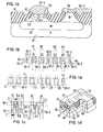
- FIG lb shows the structure of Figure la in top view with, however, a modification wherein each collector sink 46, 46-1, 46-2 and 46-3 ( Figures la and lb) is used to provide electrical contact to two active devices rather than one active device.
- collector sink C2 (46-2) makes electrical contact to the active devices including emitters E2 and E3 (numbered 45-2 and 45-3 in Figure lb).
- Buried layer 42-2 allows electrical contact from collector sink 46-2 to the two devices containing emitters E2 and E3 underneath the isolation oxide 47 surrounding each of these two active devices. Oxide 47 defines the lateral extent of these devices.
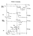
- the voltage drop circuit i.e. the circuit that detects the voltage drop Vp s following the programming of a cell
- the voltage drop circuit should be inhibited for about the first 3 microseconds during the-initialization of the current ramp due to possible overshoot of the current and drop in the voltage associated with the current as it returns to its nominal value.
- This inhibition circuit prevents the sense circuit from interpreting this drop incorrectly as indicating the programming of the cell.
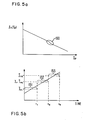
- pulse delays are measured to where the level is to change, pulse widths are measured after the level has been reached and rise and fall times are measured from 10% to 90% of amplitude.
Landscapes
- Read Only Memory (AREA)
- Semiconductor Memories (AREA)
Applications Claiming Priority (2)
| Application Number | Priority Date | Filing Date | Title |
|---|---|---|---|
| US06/349,790 US4480318A (en) | 1982-02-18 | 1982-02-18 | Method of programming of junction-programmable read-only memories |
| US349790 | 1982-02-18 |
Publications (3)
| Publication Number | Publication Date |
|---|---|
| EP0087360A2 true EP0087360A2 (de) | 1983-08-31 |
| EP0087360A3 EP0087360A3 (en) | 1986-02-05 |
| EP0087360B1 EP0087360B1 (de) | 1989-05-31 |
Family
ID=23373976
Family Applications (1)
| Application Number | Title | Priority Date | Filing Date |
|---|---|---|---|
| EP83400317A Expired EP0087360B1 (de) | 1982-02-18 | 1983-02-15 | Technik zum Programmieren von Festwertspeichern durch Veränderung der Übergänge |
Country Status (5)
| Country | Link |
|---|---|
| US (1) | US4480318A (de) |
| EP (1) | EP0087360B1 (de) |
| JP (1) | JPS58189900A (de) |
| CA (1) | CA1193009A (de) |
| DE (1) | DE3380006D1 (de) |
Cited By (1)
| Publication number | Priority date | Publication date | Assignee | Title |
|---|---|---|---|---|
| EP0574131A3 (de) * | 1992-06-09 | 1995-01-18 | Actel Corp | Hochleistungsverfahren zur Programmierung von Antischmelzsicherungen. |
Families Citing this family (10)
| Publication number | Priority date | Publication date | Assignee | Title |
|---|---|---|---|---|
| US4727409A (en) * | 1982-04-12 | 1988-02-23 | Signetics Corporation | Programmable read-only memory formed with opposing PN diodes |
| JPS59130441A (ja) * | 1982-12-25 | 1984-07-27 | Fujitsu Ltd | ヒューズ型romの書込み方法 |
| US4646427A (en) * | 1984-06-28 | 1987-03-03 | Motorola, Inc. | Method of electrically adjusting the zener knee of a lateral polysilicon zener diode |
| GB2253489B (en) * | 1991-03-06 | 1995-06-07 | Motorola Inc | Programmable read only memory |
| US5544111A (en) * | 1991-03-14 | 1996-08-06 | Gemplus Card International | Programming process for integrated memory, particularly for a smart card |
| US5465341A (en) * | 1992-10-23 | 1995-11-07 | Vlsi Technology, Inc. | Verifiable security circuitry for preventing unauthorized access to programmed read only memory |
| JP2004247578A (ja) * | 2003-02-14 | 2004-09-02 | Kawasaki Microelectronics Kk | 半導体装置および半導体装置の製造方法 |
| US8547756B2 (en) | 2010-10-04 | 2013-10-01 | Zeno Semiconductor, Inc. | Semiconductor memory device having an electrically floating body transistor |
| US8130547B2 (en) | 2007-11-29 | 2012-03-06 | Zeno Semiconductor, Inc. | Method of maintaining the state of semiconductor memory having electrically floating body transistor |
| US10340276B2 (en) | 2010-03-02 | 2019-07-02 | Zeno Semiconductor, Inc. | Method of maintaining the state of semiconductor memory having electrically floating body transistor |
Family Cites Families (12)
| Publication number | Priority date | Publication date | Assignee | Title |
|---|---|---|---|---|
| US3191151A (en) * | 1962-11-26 | 1965-06-22 | Fairchild Camera Instr Co | Programmable circuit |
| US3810127A (en) * | 1970-06-23 | 1974-05-07 | Intel Corp | Programmable circuit {13 {11 the method of programming thereof and the devices so programmed |
| US3742592A (en) * | 1970-07-13 | 1973-07-03 | Intersil Inc | Electrically alterable integrated circuit read only memory unit and process of manufacturing |
| US3733690A (en) * | 1970-07-13 | 1973-05-22 | Intersil Inc | Double junction read only memory and process of manufacture |
| US3848238A (en) * | 1970-07-13 | 1974-11-12 | Intersil Inc | Double junction read only memory |
| US3872450A (en) * | 1973-06-21 | 1975-03-18 | Motorola Inc | Fusible link memory cell for a programmable read only memory |
| US4156926A (en) * | 1976-06-01 | 1979-05-29 | Texas Instruments Incorporated | PROM circuit board programmer |
| FR2369652A1 (fr) * | 1976-10-29 | 1978-05-26 | Radiotechnique Compelec | Memoire morte programmable a transistors |
| JPS53124040A (en) * | 1977-04-06 | 1978-10-30 | Toshiba Corp | Fuse matrix memory device |
| US4145702A (en) * | 1977-07-05 | 1979-03-20 | Burroughs Corporation | Electrically programmable read-only-memory device |
| JPS5828679B2 (ja) * | 1979-04-25 | 1983-06-17 | 富士通株式会社 | 半導体記憶装置の書込み回路 |
| US4335457A (en) * | 1980-08-08 | 1982-06-15 | Fairchild Camera & Instrument Corp. | Method for semiconductor memory testing |
-
1982
- 1982-02-18 US US06/349,790 patent/US4480318A/en not_active Expired - Lifetime
-
1983
- 1983-02-15 EP EP83400317A patent/EP0087360B1/de not_active Expired
- 1983-02-15 DE DE8383400317T patent/DE3380006D1/de not_active Expired
- 1983-02-17 CA CA000421876A patent/CA1193009A/en not_active Expired
- 1983-02-18 JP JP58024962A patent/JPS58189900A/ja active Granted
Cited By (1)
| Publication number | Priority date | Publication date | Assignee | Title |
|---|---|---|---|---|
| EP0574131A3 (de) * | 1992-06-09 | 1995-01-18 | Actel Corp | Hochleistungsverfahren zur Programmierung von Antischmelzsicherungen. |
Also Published As
| Publication number | Publication date |
|---|---|
| EP0087360B1 (de) | 1989-05-31 |
| DE3380006D1 (en) | 1989-07-06 |
| CA1193009A (en) | 1985-09-03 |
| EP0087360A3 (en) | 1986-02-05 |
| JPH0247040B2 (de) | 1990-10-18 |
| US4480318A (en) | 1984-10-30 |
| JPS58189900A (ja) | 1983-11-05 |
Similar Documents
| Publication | Publication Date | Title |
|---|---|---|
| EP0528417B1 (de) | Festwertspeicher mit Anti-Sicherungselementen | |
| US7304888B2 (en) | Reverse-bias method for writing memory cells in a memory array | |
| US6897543B1 (en) | Electrically-programmable integrated circuit antifuses | |
| US4480318A (en) | Method of programming of junction-programmable read-only memories | |
| US4595875A (en) | Short detector for PROMS | |
| EP0495317A1 (de) | Mit niedriger Spannung programmierbare Antischmelzsicherung und Verfahren zu ihrer Programmierung | |
| US20050101088A1 (en) | Manufacturing method for integrated circuit having disturb-free programming of passive element memory cells | |
| EP0008946B1 (de) | Halbleiter-Speichervorrichtung | |
| US7126871B2 (en) | Circuits and methods to protect a gate dielectric antifuse | |
| KR0122103B1 (ko) | 반도체 메모리 장치의 퓨즈 소자 | |
| US4347586A (en) | Semiconductor memory device | |
| GB1571424A (en) | Semiconductor memories | |
| US8842488B2 (en) | Low voltage efuse programming circuit and method | |
| US4719599A (en) | Programmable read-only memory device provided with test cells | |
| US4399450A (en) | ROM With poly-Si to mono-Si diodes | |
| US7126204B2 (en) | Integrated semiconductor circuit with an electrically programmable switching element | |
| US4432070A (en) | High speed PROM device | |
| US4769785A (en) | Writing speed of SCR-based memory cells | |
| US4045784A (en) | Programmable read only memory integrated circuit device | |
| US4153949A (en) | Electrically programmable read-only-memory device | |
| US6979602B1 (en) | Method for making a recessed thyristor control port | |
| US7465965B2 (en) | Transistor controlled thyristor memory device | |
| US20020050606A1 (en) | Semi-monolithic memory with high-density cell configurations | |
| US20050133882A1 (en) | Integrated circuit fuse and method of fabrication | |
| US4399521A (en) | Monolithic integrated circuit |
Legal Events
| Date | Code | Title | Description |
|---|---|---|---|
| PUAI | Public reference made under article 153(3) epc to a published international application that has entered the european phase |
Free format text: ORIGINAL CODE: 0009012 |
|
| AK | Designated contracting states |
Designated state(s): DE FR GB IT NL |
|
| PUAL | Search report despatched |
Free format text: ORIGINAL CODE: 0009013 |
|
| AK | Designated contracting states |
Designated state(s): DE FR GB IT NL |
|
| 17P | Request for examination filed |
Effective date: 19860730 |
|
| 17Q | First examination report despatched |
Effective date: 19871221 |
|
| RAP1 | Party data changed (applicant data changed or rights of an application transferred) |
Owner name: FAIRCHILD SEMICONDUCTOR CORPORATION |
|
| GRAA | (expected) grant |
Free format text: ORIGINAL CODE: 0009210 |
|
| AK | Designated contracting states |
Kind code of ref document: B1 Designated state(s): DE FR GB IT NL |
|
| REF | Corresponds to: |
Ref document number: 3380006 Country of ref document: DE Date of ref document: 19890706 |
|
| ET | Fr: translation filed | ||
| ITF | It: translation for a ep patent filed | ||
| PLBE | No opposition filed within time limit |
Free format text: ORIGINAL CODE: 0009261 |
|
| STAA | Information on the status of an ep patent application or granted ep patent |
Free format text: STATUS: NO OPPOSITION FILED WITHIN TIME LIMIT |
|
| 26N | No opposition filed | ||
| ITTA | It: last paid annual fee | ||
| PGFP | Annual fee paid to national office [announced via postgrant information from national office to epo] |
Ref country code: GB Payment date: 19940110 Year of fee payment: 12 |
|
| PGFP | Annual fee paid to national office [announced via postgrant information from national office to epo] |
Ref country code: FR Payment date: 19940211 Year of fee payment: 12 |
|
| PGFP | Annual fee paid to national office [announced via postgrant information from national office to epo] |
Ref country code: NL Payment date: 19940228 Year of fee payment: 12 |
|
| PG25 | Lapsed in a contracting state [announced via postgrant information from national office to epo] |
Ref country code: GB Effective date: 19950215 |
|
| PG25 | Lapsed in a contracting state [announced via postgrant information from national office to epo] |
Ref country code: NL Effective date: 19950901 |
|
| GBPC | Gb: european patent ceased through non-payment of renewal fee |
Effective date: 19950215 |
|
| PG25 | Lapsed in a contracting state [announced via postgrant information from national office to epo] |
Ref country code: FR Effective date: 19951031 |
|
| NLV4 | Nl: lapsed or anulled due to non-payment of the annual fee |
Effective date: 19950901 |
|
| REG | Reference to a national code |
Ref country code: FR Ref legal event code: ST |
|
| PGFP | Annual fee paid to national office [announced via postgrant information from national office to epo] |
Ref country code: DE Payment date: 20020118 Year of fee payment: 20 |