EP0087312A2 - Formation de régions de différents types de conduction dans un substrat - Google Patents
Formation de régions de différents types de conduction dans un substrat Download PDFInfo
- Publication number
- EP0087312A2 EP0087312A2 EP83300900A EP83300900A EP0087312A2 EP 0087312 A2 EP0087312 A2 EP 0087312A2 EP 83300900 A EP83300900 A EP 83300900A EP 83300900 A EP83300900 A EP 83300900A EP 0087312 A2 EP0087312 A2 EP 0087312A2
- Authority
- EP
- European Patent Office
- Prior art keywords
- substrate
- regions
- forming
- conductivity type
- mask
- Prior art date
- Legal status (The legal status is an assumption and is not a legal conclusion. Google has not performed a legal analysis and makes no representation as to the accuracy of the status listed.)
- Withdrawn
Links
Images

Classifications
-
- H—ELECTRICITY
- H01—ELECTRIC ELEMENTS
- H01L—SEMICONDUCTOR DEVICES NOT COVERED BY CLASS H10
- H01L21/00—Processes or apparatus adapted for the manufacture or treatment of semiconductor or solid state devices or of parts thereof
- H01L21/70—Manufacture or treatment of devices consisting of a plurality of solid state components formed in or on a common substrate or of parts thereof; Manufacture of integrated circuit devices or of parts thereof
- H01L21/77—Manufacture or treatment of devices consisting of a plurality of solid state components or integrated circuits formed in, or on, a common substrate
- H01L21/78—Manufacture or treatment of devices consisting of a plurality of solid state components or integrated circuits formed in, or on, a common substrate with subsequent division of the substrate into plural individual devices
- H01L21/82—Manufacture or treatment of devices consisting of a plurality of solid state components or integrated circuits formed in, or on, a common substrate with subsequent division of the substrate into plural individual devices to produce devices, e.g. integrated circuits, each consisting of a plurality of components
- H01L21/822—Manufacture or treatment of devices consisting of a plurality of solid state components or integrated circuits formed in, or on, a common substrate with subsequent division of the substrate into plural individual devices to produce devices, e.g. integrated circuits, each consisting of a plurality of components the substrate being a semiconductor, using silicon technology
- H01L21/8232—Field-effect technology
- H01L21/8234—MIS technology, i.e. integration processes of field effect transistors of the conductor-insulator-semiconductor type
- H01L21/8238—Complementary field-effect transistors, e.g. CMOS
-
- H—ELECTRICITY
- H01—ELECTRIC ELEMENTS
- H01L—SEMICONDUCTOR DEVICES NOT COVERED BY CLASS H10
- H01L21/00—Processes or apparatus adapted for the manufacture or treatment of semiconductor or solid state devices or of parts thereof
- H01L21/02—Manufacture or treatment of semiconductor devices or of parts thereof
- H01L21/027—Making masks on semiconductor bodies for further photolithographic processing not provided for in group H01L21/18 or H01L21/34
- H01L21/033—Making masks on semiconductor bodies for further photolithographic processing not provided for in group H01L21/18 or H01L21/34 comprising inorganic layers
-
- Y—GENERAL TAGGING OF NEW TECHNOLOGICAL DEVELOPMENTS; GENERAL TAGGING OF CROSS-SECTIONAL TECHNOLOGIES SPANNING OVER SEVERAL SECTIONS OF THE IPC; TECHNICAL SUBJECTS COVERED BY FORMER USPC CROSS-REFERENCE ART COLLECTIONS [XRACs] AND DIGESTS
- Y10—TECHNICAL SUBJECTS COVERED BY FORMER USPC
- Y10S—TECHNICAL SUBJECTS COVERED BY FORMER USPC CROSS-REFERENCE ART COLLECTIONS [XRACs] AND DIGESTS
- Y10S438/00—Semiconductor device manufacturing: process
- Y10S438/983—Zener diodes
Definitions
- This invention relates to methods of forming regions of different conductivity types in a substrate, for example methods of fabricating CMOS semiconductor devices.
- a method of forming regions of different conductivities within a substrate comprising the steps of forming a mask on the surface of said substrate to expose only those regions of said substrate where it is desired to introduce a dopant of a first conductivity type, introducing dopant of said first conductivity into said substrate, wherein said dopant is formed within only said exposed region, characterized by comprising the additional steps of :
- the invention also provides a method of forming a complementary metal oxide-silicon (CMOS) device within a substrate of first conductivity type comprising the steps of forming a well region of a second conductivity type opposite said first conductivity type within said substrate, forming a field region in all areas in which active devices are not to be formed, thus exposing active regions on the surface of said substrate in which active devices are to be formed, forming a gate insulation layer within said active regions, forming a gate region on said gate insulation layer, masking said substrate with a first protective layer, patterning said dust protective layer to expose only those active regions within said well region, doping regions to said first conductivity type within said well region which are not protected by said gate region or said field region, said method characterized by comprising the steps of:
- a fabrication method can be provided which allows the formation of regions of opposite conductivity types utilizing a single masking step.
- the method can comprise the following steps.
- a first mask is formed on the surface of the semiconductor substrate and patterned to define the regions which are to be doped to a first conductivity type.
- a protective layer is formed over these first regions.
- these protective layers are not grown on any regions other than those regions which have been doped to said first conductivity type.
- the mask is removed, thus exposing the regions which are to be doped to the second conductivity type opposite to said first conductivity type.
- CMOS complementary metal oxide silicon
- CMOS Complementary Metal Oxide Silicon
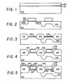
- a semiconductor substrate 100 such as an N type silicon wafer having conductivity of approximately 3 to 5 ohm-cm is used as the. starting material.
- Base oxide 101 is grown to a thickness 0 of approximately 500A by thermal oxidation, such as oxidation in oxygen for approximately 35 minutes at approximately 1000°C.
- silicon nitride layer 102 is deposited to a thickness of ° approximately 1500A.
- Silicon nitride layer 102 is deposited in a manner well known in the semiconductor arts, such as by a low pressure chemical vapor deposition such as is described by Roessler, in Solid State Technology, April 1977, page 63 and by Brown, et al, in Solid State Technology, July 1979, page 51.
- base oxide layer 101 and silicon nitride layer 102 are patterned utilizing well-known photolithographic and etching techniques in order to pattern oxide layer 101 and silicon nitride layer 102 to expose the surface of substrate 100 where field oxide is to be subsequently formed.
- Silicon nitride layer l02 is patterned, for example, by etching with CF 4 plasma.
- oxide layer 101 is patterned by etching with, for example, buffered hydrofluoric acid.
- a first layer of masking material (not shown) is applied to the surface of the wafer and patterned in a well-known manner to expose the to-be-formed P well region 103.
- the P well region 103 then is formed, for example, by a two step implanation of boron ions consisting of a first implant of boron atoms at an energy level of approximately 25 KeV followed by a second implant of boron ions at approximately 90 KeV, thus (after dopant drive, as described more fully later) forming a P well region having a dopant concentration of boron atoms of approximately 3x10 16 atoms/cm 3 .
- the use of a two step P-well implant is described in U.S. Patent No. 4306916 issued 22 December 1981 and assigned to American Microsystems, Inc., which is hereby incorporated by reference. This doping procedure also serves to establish the desired P-well field inversion threshold voltage in a well known manner.
- the first layer of masking material is then removed from the surface of the wafer.
- a second layer of masking material (not shown) is applied to the surface of the wafer and patterned to expose those regions of the wafer where there is to be no P-well.
- An N type dopant for example arsenic, is then deposited in these regions as indicated by regions 104 in Figure 2.
- N type regions 104 form guard rings to provide isolation between N channel devices formed within P well 103, and P channel devices formed within substrate 100. These N-type dopants also serve to establish the desired substrate field inversion voltage in a well known manner.
- This N type dopant is performed, for example, by an implantation of arsenic ions at an energy level of approximately 40 KeV, thus resulting in a dopant concentration of approximately 1.53x10 12 atoms/cm 2 within regions 104.
- field'oxide 105 is then thermally grown to a thickness of approximately 1-2 microns.
- This field oxide is grown, for example, by oxidation in steam for 14 hours at approximately 1000°C, during which time the P type dopants deposited in the P-well and the N type dopants deposited in the substrate are diffused, thus establishing the desired dopant profile (the dopant concentration with respect to distance from the device surface) within the P-well and the substrate.
- oxide layer 101 and nitride layer 102 Figure 2
- silicon nitride layer 102 is removed, for example, by etching with a CF 4 plasma.
- Oxide region 101 is then removed, for example, by etching in buffered hydrofluoric acid. During the removal of oxide region 101, a small decrease in the thickness of field oxide 105 occurs. However, because field oxide 105 is extremely thick relative to the thickness of oxide layer 101, this slight decrease in the thickness of field oxide 105 is unimportant, and may be ignored.
- Gate oxide 106 ( Figure 3) is then formed to a thick-0 ness of approximately 500-1000A by thermal oxidation in steam for approximately 15 minutes at approximately 1000° C , for example. During the formation of gate oxide 106, the thickness of field oxide regions 105 is increased slightly, although this slight increase in the thickness of field oxide 105 may be ignored.
- a layer of polycrystalline silicon 107 is deposited on the surface of the wafer.
- Polycrystalline silicon 107 is then doped to reduce its sheet resistance to approximately 30 ohms/square, for example by doping with phosphorus by applying to the wafer POC1 3 for 12 minutes at approximately 970°C.
- Polycrystalline silicon layer 107 is formed to a thickness of approximately 4,OOOA. by, for example, low pressure chemical deposition, as described by Saraswat, et al in Journal of the Electrochemical Society, Number 125, page 927 (1978).
- Polycrystalline silicon region 107 is then oxidized, 0 thus forming an oxide layer 108 of approximately 1,000 A thickness.
- Polycrystalline silicon 107 is oxidized, for example, by wet oxidation (oxidation in steam) for approximately 7 minutes at approximately 950°C.
- Polycrystalline silicon 107 and oxide 108 are then patterned into gate regions overlying gate oxide 106, as shown in Figure 4.
- Oxide layer 108 and polycrystalline silicon are patterned utilizing well-known masking techniques, for example, etching oxide 108 with buffered HF and etching.
- Polycrystalline silicon 107 with, for example, CF 4 plasma Thus polycrystalline gates 107 and oxide 108 are formed as shown in Figure 4.
- the gate oxide 106 surrounding gate regions 107 is removed, for example by etching with buffered HF. ° A thin (approximately 130A) layer of oxide (not shown) is then formed over the entire surface of the wafer to prevent damage to the silicon underlying the to-be-formed nitride layer 109. This oxide is formed, for example, by oxidation in dry oxygen for 10 minutes at approximately 950°C. A layer of silicon nitride 109 (Fig. 5) is then deposited on the surface of the wafer and patterned to expose that portion of the wafer in which regions of a first conductivity type are to be formed.
- Silicon nitride layer ° 109 is formed to a thickness of approximately 700 A. by, for example, low-pressure chemical vapor deposition, such as described in the aforementioned article by Roessler and Brown. Silicon nitride layer 109 is then patterned as shown in Figure 5 to expose the surface of the wafer containing P well 103. Silicon nitride layer 109 may be patterned by utilizing well-known photolithographic masking techniques and etching undesired portions of silicon nitride 109 with, for example, CF 4 plasma. Source and drain regions are then formed within P well 103 by doping regions 110 with an N type dopant, such as phosphorous. Regions l10 of N type conductivity are formed, for example, by gaseous deposition of POC1 3 for 3 minutes at approximately 970°C or, alternatively, by the ion implantation of phosphorus or arsenic atoms.
- N type dopant such as phosphorous
- a thin layer of o oxide 111 (approximately 1200 A) is formed over source/drain regions 110.
- Oxide regions 111 are formed, for example, by thermal oxidation in steam for approximately 3 minutes at approximately 1050 0 C.
- the exposed oxide regions 108 and the exposed field oxide regions 105 (exposed being those regions not covered by silicon nitride layer 109 shown in Figure 5), are also oxidized, thus increasing their thickness slightly. This slight increase in the thickness of exposed oxide regions 105 and 108 is unimportant and may be ignored.
- the formation of oxide region 111 serves to protect regions 110 from subsequent doping, thus eliminating the need for a second mask to be formed over the surface of the wafer and patterned to expose to-be-formed P regions 112, while protecting N regions 110.
- silicon nitride layer 109 ( Figure 5) is removed, for example, by etching with CF 4 plasma.
- the very thin layer of oxide formed on the silicon nitride 109 during the formation of oxide regions 111 is also removed by the CF 4 plasma.
- Those portions of thin oxide covering the to-be-formed P type conductivity regions 112 are then removed, for example, by etching in buffered hydrofluoric acid.
- field oxide regions 105, oxide regions 108, and protective oxide regions 111 are also etched.
- thin oxide 106 is completely removed while leaving intact, although slightly thinner, field oxide 105, oxide 108, and protective oxide 111.
- Regions 112 of P type conductivity may now be formed in substrate 100 as shown in Figure 6.
- P type regions are formed, for example, by doping with boron, from a gaseous BBr 3 source for 8 minutes at approximately 1075°C or by low energy (e.g. 30-70 keV) ion implantation of boron atoms.
- the boron source is applied on the surface of the entire wafer.
- boron enters only in regions 112, because all other portions of the wafer are protected from boron deposition by either field oxide regions 105, the gate structure comprised of gate oxide 106, polycrystalline gate 107, and oxide 108, or by protective oxide 111 formed above N type regions 110.
- N type regions 110 and P type regions 112 are formed in a semiconductor substrate utilizing a single photolithographic masking step.
- the formation of such N type regions and P type regions in a wafer was heretofore generally possible only by the use of two separate masking steps, requiring an increased number of process steps, as well as a resultant increase in cost.
- Prior art one-mask introduction of N type and P type dopants utilizing phosphorus doped oxide cannot be easily used to fabricate semiconductor devices of small (less than 5 micron line width) devices.
- a layer of isolation oxide 113 is 0 formed to a thickness of approximately 10,000A over the entire surface of the wafer, such as, for example, by chemical vapor deposition.
- Contact openings are then formed, as shown in Figure 7, through isolation oxide 113, thus allowing electrical contact to be made to source region 112a of Figure 7.
- a contact opening is made in isolation oxide 113 and protective oxide 108, thus allowing contact to be made to polycrystalline silicon gate region 107.
- contact openings through isolation oxide l13 and various other oxides within the structure is performed in a conventional manner, utilizing suitable prior art photolithographic masking techniques and etching the exposed oxide layers with, for example, buffered hydrofluoric acid.
- a layer of metallization 114 is formed on the surface of the wafer.
- Metallization 114 is preferably aluminum formed in a conventional manner.
- the metallization layer 114 is then patterned, such as by utilizing well-known photolithographic techniques, and etching undesired portions of metallization 114 with, for example, an etching solution comprised of acetic, nitric and phosphoric acids.
- a substrate is masked in a well known manner (e.g. by photoresist) to expose a first region.
- a dopant of a first conductivity type is introduced into the first region exposed by the mask.
- a protective layer e.g. silicon dioxide or silicon nitride
- a dopant of a second conductivity type opposite said first conductivity type is introduced into the region previously protected by the mask and now exposed by the protective layer.
- a substrate is masked in a well known manner (e.g. by photoresist) to expose a first region.
- a dopant of a first conductivity type is introduced into the first region exposed by the mask.
- a protective layer e.g. silicon dioxide or silicon nitride
- a dopant of said first conductivity type but to a different dosage is introduced into the region previously protected by the mask and now exposed by the protective layer.
Landscapes
- Engineering & Computer Science (AREA)
- Physics & Mathematics (AREA)
- Condensed Matter Physics & Semiconductors (AREA)
- General Physics & Mathematics (AREA)
- Manufacturing & Machinery (AREA)
- Computer Hardware Design (AREA)
- Microelectronics & Electronic Packaging (AREA)
- Power Engineering (AREA)
- Chemical & Material Sciences (AREA)
- Inorganic Chemistry (AREA)
- Metal-Oxide And Bipolar Metal-Oxide Semiconductor Integrated Circuits (AREA)
- Light Receiving Elements (AREA)
Applications Claiming Priority (2)
| Application Number | Priority Date | Filing Date | Title |
|---|---|---|---|
| US06/351,075 US4450021A (en) | 1982-02-22 | 1982-02-22 | Mask diffusion process for forming Zener diode or complementary field effect transistors |
| US351075 | 1982-02-22 |
Publications (2)
| Publication Number | Publication Date |
|---|---|
| EP0087312A2 true EP0087312A2 (fr) | 1983-08-31 |
| EP0087312A3 EP0087312A3 (fr) | 1985-04-03 |
Family
ID=23379466
Family Applications (1)
| Application Number | Title | Priority Date | Filing Date |
|---|---|---|---|
| EP83300900A Withdrawn EP0087312A3 (fr) | 1982-02-22 | 1983-02-21 | Formation de régions de différents types de conduction dans un substrat |
Country Status (5)
| Country | Link |
|---|---|
| US (1) | US4450021A (fr) |
| EP (1) | EP0087312A3 (fr) |
| JP (1) | JPS58155737A (fr) |
| CA (1) | CA1198227A (fr) |
| DE (1) | DE87312T1 (fr) |
Cited By (1)
| Publication number | Priority date | Publication date | Assignee | Title |
|---|---|---|---|---|
| US5089427A (en) * | 1990-12-03 | 1992-02-18 | Motorola Inc. | Semiconductor device and method |
Families Citing this family (14)
| Publication number | Priority date | Publication date | Assignee | Title |
|---|---|---|---|---|
| US4511413A (en) * | 1983-10-05 | 1985-04-16 | Analog Devices, Incorporated | Process for forming an IC wafer with buried Zener diodes |
| US4567640A (en) * | 1984-05-22 | 1986-02-04 | Data General Corporation | Method of fabricating high density CMOS devices |
| US4621412A (en) * | 1984-09-17 | 1986-11-11 | Sony Corporation | Manufacturing a complementary MOSFET |
| US4709253A (en) * | 1986-05-02 | 1987-11-24 | Amp Incorporated | Surface mountable diode |
| US4874714A (en) * | 1988-06-02 | 1989-10-17 | Texas Instruments Incorporated | Method of making laterally oriented Schottky diode |
| US5514616A (en) * | 1991-08-26 | 1996-05-07 | Lsi Logic Corporation | Depositing and densifying glass to planarize layers in semi-conductor devices based on CMOS structures |
| US5641708A (en) * | 1994-06-07 | 1997-06-24 | Sgs-Thomson Microelectronics, Inc. | Method for fabricating conductive structures in integrated circuits |
| US5498570A (en) * | 1994-09-15 | 1996-03-12 | Micron Technology Inc. | Method of reducing overetch during the formation of a semiconductor device |
| US6153501A (en) | 1998-05-19 | 2000-11-28 | Micron Technology, Inc. | Method of reducing overetch during the formation of a semiconductor device |
| US5783470A (en) * | 1995-12-14 | 1998-07-21 | Lsi Logic Corporation | Method of making CMOS dynamic random-access memory structures and the like |
| US6051501A (en) * | 1996-10-09 | 2000-04-18 | Micron Technology, Inc. | Method of reducing overetch during the formation of a semiconductor device |
| US6821852B2 (en) * | 2001-02-13 | 2004-11-23 | Micron Technology, Inc. | Dual doped gates |
| US20080258263A1 (en) * | 2007-04-20 | 2008-10-23 | Harry Yue Gee | High Current Steering ESD Protection Zener Diode And Method |
| US8518782B2 (en) | 2010-12-08 | 2013-08-27 | International Business Machines Corporation | Semiconductor device including asymmetric lightly doped drain (LDD) region, related method and design structure |
Citations (7)
| Publication number | Priority date | Publication date | Assignee | Title |
|---|---|---|---|---|
| DE1931201A1 (de) * | 1968-06-27 | 1970-02-12 | Philips Nv | Verfahren zur Herstellung einer Zenerdiode |
| US4033797A (en) * | 1973-05-21 | 1977-07-05 | Hughes Aircraft Company | Method of manufacturing a complementary metal-insulation-semiconductor circuit |
| US4067037A (en) * | 1976-04-12 | 1978-01-03 | Massachusetts Institute Of Technology | Transistor having high ft at low currents |
| US4115797A (en) * | 1976-10-04 | 1978-09-19 | Fairchild Camera And Instrument Corporation | Integrated injection logic with heavily doped injector base self-aligned with injector emitter and collector |
| US4168999A (en) * | 1978-12-26 | 1979-09-25 | Fairchild Camera And Instrument Corporation | Method for forming oxide isolated integrated injection logic semiconductor structures having minimal encroachment utilizing special masking techniques |
| DE2933849A1 (de) * | 1978-08-23 | 1980-03-13 | Hitachi Ltd | Verfahren zur herstellung von halbleiteranordnungen |
| EP0072967A2 (fr) * | 1981-08-25 | 1983-03-02 | Siemens Aktiengesellschaft | Procédé pour la fabrication de circuits à transistors à effet de champ complémentaire à haute densité d'intégration en technologie d'électrode de porte en silicium |
Family Cites Families (8)
| Publication number | Priority date | Publication date | Assignee | Title |
|---|---|---|---|---|
| US3928081A (en) * | 1973-10-26 | 1975-12-23 | Signetics Corp | Method for fabricating semiconductor devices using composite mask and ion implantation |
| US4099998A (en) * | 1975-11-03 | 1978-07-11 | General Electric Company | Method of making zener diodes with selectively variable breakdown voltages |
| IT1166587B (it) * | 1979-01-22 | 1987-05-05 | Ates Componenti Elettron | Processo per la fabbricazione di transistori mos complementari ad alta integrazione per tensioni elevate |
| US4306916A (en) * | 1979-09-20 | 1981-12-22 | American Microsystems, Inc. | CMOS P-Well selective implant method |
| US4295897B1 (en) * | 1979-10-03 | 1997-09-09 | Texas Instruments Inc | Method of making cmos integrated circuit device |
| JPS56124270A (en) * | 1980-03-05 | 1981-09-29 | Hitachi Ltd | Manufacture of semiconductor device |
| US4381956A (en) * | 1981-04-06 | 1983-05-03 | Motorola, Inc. | Self-aligned buried channel fabrication process |
| US4382827A (en) * | 1981-04-27 | 1983-05-10 | Ncr Corporation | Silicon nitride S/D ion implant mask in CMOS device fabrication |
-
1982
- 1982-02-22 US US06/351,075 patent/US4450021A/en not_active Expired - Lifetime
-
1983
- 1983-02-10 CA CA000421329A patent/CA1198227A/fr not_active Expired
- 1983-02-21 EP EP83300900A patent/EP0087312A3/fr not_active Withdrawn
- 1983-02-21 DE DE198383300900T patent/DE87312T1/de active Pending
- 1983-02-22 JP JP58027124A patent/JPS58155737A/ja active Pending
Patent Citations (7)
| Publication number | Priority date | Publication date | Assignee | Title |
|---|---|---|---|---|
| DE1931201A1 (de) * | 1968-06-27 | 1970-02-12 | Philips Nv | Verfahren zur Herstellung einer Zenerdiode |
| US4033797A (en) * | 1973-05-21 | 1977-07-05 | Hughes Aircraft Company | Method of manufacturing a complementary metal-insulation-semiconductor circuit |
| US4067037A (en) * | 1976-04-12 | 1978-01-03 | Massachusetts Institute Of Technology | Transistor having high ft at low currents |
| US4115797A (en) * | 1976-10-04 | 1978-09-19 | Fairchild Camera And Instrument Corporation | Integrated injection logic with heavily doped injector base self-aligned with injector emitter and collector |
| DE2933849A1 (de) * | 1978-08-23 | 1980-03-13 | Hitachi Ltd | Verfahren zur herstellung von halbleiteranordnungen |
| US4168999A (en) * | 1978-12-26 | 1979-09-25 | Fairchild Camera And Instrument Corporation | Method for forming oxide isolated integrated injection logic semiconductor structures having minimal encroachment utilizing special masking techniques |
| EP0072967A2 (fr) * | 1981-08-25 | 1983-03-02 | Siemens Aktiengesellschaft | Procédé pour la fabrication de circuits à transistors à effet de champ complémentaire à haute densité d'intégration en technologie d'électrode de porte en silicium |
Cited By (1)
| Publication number | Priority date | Publication date | Assignee | Title |
|---|---|---|---|---|
| US5089427A (en) * | 1990-12-03 | 1992-02-18 | Motorola Inc. | Semiconductor device and method |
Also Published As
| Publication number | Publication date |
|---|---|
| CA1198227A (fr) | 1985-12-17 |
| DE87312T1 (de) | 1984-02-16 |
| US4450021A (en) | 1984-05-22 |
| JPS58155737A (ja) | 1983-09-16 |
| EP0087312A3 (fr) | 1985-04-03 |
Similar Documents
| Publication | Publication Date | Title |
|---|---|---|
| US4717683A (en) | CMOS process | |
| EP0456318B1 (fr) | Procédé du type CMOS utilisant des espaceurs de nitrure de silicium placés temporairement pour faire des transistors à drains faiblement dopés | |
| US4078947A (en) | Method for forming a narrow channel length MOS field effect transistor | |
| EP0409561B1 (fr) | Méthodes de fabrication d'éléments semi-conducteurs du type MIS | |
| EP0996975B1 (fr) | Methode de fabrication d'un transistor a effet de champ en carbure de silicium | |
| US4512073A (en) | Method of forming self-aligned contact openings | |
| US5780330A (en) | Selective diffusion process for forming both n-type and p-type gates with a single masking step | |
| EP0054163B1 (fr) | Procédé de fabrication d'un contact électrique sur un substrat en silicium à travers une couche relativement mince de dioxyde de silicium formée sur la surface du substrat et procédé pour la fabrication d'un transistor à effet de champ | |
| EP0087312A2 (fr) | Formation de régions de différents types de conduction dans un substrat | |
| US5028564A (en) | Edge doping processes for mesa structures in SOS and SOI devices | |
| EP0356202B1 (fr) | Transistor à effet de champ MOS et procédé pour sa fabrication | |
| US5026663A (en) | Method of fabricating a structure having self-aligned diffused junctions | |
| US6486012B1 (en) | Semiconductor device having field effect transistors different in thickness of gate electrodes and process of fabrication thereof | |
| US4473941A (en) | Method of fabricating zener diodes | |
| US5001081A (en) | Method of manufacturing a polysilicon emitter and a polysilicon gate using the same etch of polysilicon on a thin gate oxide | |
| JPS62130558A (ja) | 集積回路装置の製法 | |
| US4600445A (en) | Process for making self aligned field isolation regions in a semiconductor substrate | |
| KR950021768A (ko) | 실드 확산 접합을 갖는 전계 효과 트랜지스터 | |
| US4409726A (en) | Method of making well regions for CMOS devices | |
| EP0337823A2 (fr) | Transistor à effet de champ ayant une tension de claquage élevée | |
| WO1984000850A1 (fr) | Procede de fabrication de contacts de circuits integres | |
| US5179031A (en) | Method of manufacturing a polysilicon emitter and a polysilicon gate using the same etch of polysilicon on a thin gate oxide | |
| US4350991A (en) | Narrow channel length MOS field effect transistor with field protection region for reduced source-to-substrate capacitance | |
| US5326713A (en) | Buried contact process | |
| US5946577A (en) | Method of manufacturing semiconductor device |
Legal Events
| Date | Code | Title | Description |
|---|---|---|---|
| PUAI | Public reference made under article 153(3) epc to a published international application that has entered the european phase |
Free format text: ORIGINAL CODE: 0009012 |
|
| AK | Designated contracting states |
Designated state(s): DE FR GB IT NL SE |
|
| ITCL | It: translation for ep claims filed |
Representative=s name: DE DOMINICIS & PARTNERS |
|
| TCNL | Nl: translation of patent claims filed | ||
| EL | Fr: translation of claims filed | ||
| DET | De: translation of patent claims | ||
| PUAL | Search report despatched |
Free format text: ORIGINAL CODE: 0009013 |
|
| 17P | Request for examination filed |
Effective date: 19841220 |
|
| AK | Designated contracting states |
Designated state(s): DE FR GB IT NL SE |
|
| 17Q | First examination report despatched |
Effective date: 19860625 |
|
| R17C | First examination report despatched (corrected) |
Effective date: 19870309 |
|
| STAA | Information on the status of an ep patent application or granted ep patent |
Free format text: STATUS: THE APPLICATION HAS BEEN WITHDRAWN |
|
| 18W | Application withdrawn |
Withdrawal date: 19871224 |
|
| RIN1 | Information on inventor provided before grant (corrected) |
Inventor name: BATRA, TARSAIM LAL Inventor name: BOWDEN, SCOTT |