EP0082787B1 - Photodiode à zones d'absorption et d'avalanche séparées - Google Patents
Photodiode à zones d'absorption et d'avalanche séparées Download PDFInfo
- Publication number
- EP0082787B1 EP0082787B1 EP82402340A EP82402340A EP0082787B1 EP 0082787 B1 EP0082787 B1 EP 0082787B1 EP 82402340 A EP82402340 A EP 82402340A EP 82402340 A EP82402340 A EP 82402340A EP 0082787 B1 EP0082787 B1 EP 0082787B1
- Authority
- EP
- European Patent Office
- Prior art keywords
- layer
- avalanche
- electric field
- forbidden band
- substrate
- Prior art date
- Legal status (The legal status is an assumption and is not a legal conclusion. Google has not performed a legal analysis and makes no representation as to the accuracy of the status listed.)
- Expired
Links
- 238000010521 absorption reaction Methods 0.000 title claims description 20
- 230000005684 electric field Effects 0.000 claims description 27
- 239000000758 substrate Substances 0.000 claims description 23
- 239000000463 material Substances 0.000 claims description 18
- 238000001465 metallisation Methods 0.000 claims description 13
- 229910005542 GaSb Inorganic materials 0.000 claims description 3
- 239000013078 crystal Substances 0.000 claims description 2
- 230000001960 triggered effect Effects 0.000 claims 2
- 239000010410 layer Substances 0.000 description 82
- 230000003321 amplification Effects 0.000 description 6
- 238000003199 nucleic acid amplification method Methods 0.000 description 6
- 239000004065 semiconductor Substances 0.000 description 6
- 238000010586 diagram Methods 0.000 description 5
- 230000000694 effects Effects 0.000 description 5
- 239000013307 optical fiber Substances 0.000 description 4
- 238000001514 detection method Methods 0.000 description 3
- 238000009792 diffusion process Methods 0.000 description 3
- 230000031700 light absorption Effects 0.000 description 3
- 230000010287 polarization Effects 0.000 description 3
- 229910000530 Gallium indium arsenide Inorganic materials 0.000 description 2
- 240000008042 Zea mays Species 0.000 description 2
- 238000013459 approach Methods 0.000 description 2
- 150000001875 compounds Chemical class 0.000 description 2
- 238000002513 implantation Methods 0.000 description 2
- 239000012535 impurity Substances 0.000 description 2
- 230000003595 spectral effect Effects 0.000 description 2
- 238000005513 bias potential Methods 0.000 description 1
- 230000005540 biological transmission Effects 0.000 description 1
- 239000000969 carrier Substances 0.000 description 1
- 230000015556 catabolic process Effects 0.000 description 1
- 239000002800 charge carrier Substances 0.000 description 1
- 230000007423 decrease Effects 0.000 description 1
- 239000002019 doping agent Substances 0.000 description 1
- 229910052732 germanium Inorganic materials 0.000 description 1
- GNPVGFCGXDBREM-UHFFFAOYSA-N germanium atom Chemical compound [Ge] GNPVGFCGXDBREM-UHFFFAOYSA-N 0.000 description 1
- 230000000977 initiatory effect Effects 0.000 description 1
- 238000009830 intercalation Methods 0.000 description 1
- 238000005259 measurement Methods 0.000 description 1
- 238000012986 modification Methods 0.000 description 1
- 230000004048 modification Effects 0.000 description 1
- 238000005457 optimization Methods 0.000 description 1
- 238000001228 spectrum Methods 0.000 description 1
- 239000002344 surface layer Substances 0.000 description 1
- 238000000927 vapour-phase epitaxy Methods 0.000 description 1
Images
Classifications
-
- H—ELECTRICITY
- H10—SEMICONDUCTOR DEVICES; ELECTRIC SOLID-STATE DEVICES NOT OTHERWISE PROVIDED FOR
- H10F—INORGANIC SEMICONDUCTOR DEVICES SENSITIVE TO INFRARED RADIATION, LIGHT, ELECTROMAGNETIC RADIATION OF SHORTER WAVELENGTH OR CORPUSCULAR RADIATION
- H10F30/00—Individual radiation-sensitive semiconductor devices in which radiation controls the flow of current through the devices, e.g. photodetectors
- H10F30/20—Individual radiation-sensitive semiconductor devices in which radiation controls the flow of current through the devices, e.g. photodetectors the devices having potential barriers, e.g. phototransistors
- H10F30/21—Individual radiation-sensitive semiconductor devices in which radiation controls the flow of current through the devices, e.g. photodetectors the devices having potential barriers, e.g. phototransistors the devices being sensitive to infrared, visible or ultraviolet radiation
- H10F30/22—Individual radiation-sensitive semiconductor devices in which radiation controls the flow of current through the devices, e.g. photodetectors the devices having potential barriers, e.g. phototransistors the devices being sensitive to infrared, visible or ultraviolet radiation the devices having only one potential barrier, e.g. photodiodes
- H10F30/225—Individual radiation-sensitive semiconductor devices in which radiation controls the flow of current through the devices, e.g. photodetectors the devices having potential barriers, e.g. phototransistors the devices being sensitive to infrared, visible or ultraviolet radiation the devices having only one potential barrier, e.g. photodiodes the potential barrier working in avalanche mode, e.g. avalanche photodiodes
- H10F30/2255—Individual radiation-sensitive semiconductor devices in which radiation controls the flow of current through the devices, e.g. photodetectors the devices having potential barriers, e.g. phototransistors the devices being sensitive to infrared, visible or ultraviolet radiation the devices having only one potential barrier, e.g. photodiodes the potential barrier working in avalanche mode, e.g. avalanche photodiodes in which the active layers form heterostructures, e.g. SAM structures
Definitions
- the invention relates to a photodiode with separate absorption and avalanche zones, operating in the 1.2-1.6 micron range, produced using materials of families III-V, and having a high avalanche gain, although the noise factor is low.
- the invention relates more precisely to the structure of the semiconductor layers which constitute an avalanche photodiode: the optimization of this structure, by geometrical modifications of the layers or making of contact for example, is part of the knowledge of the art and certain improvements.
- Avalanche photodiodes are already known, for example patent applications FR-A-2 311 408, FR-A-2 396 419 and FR-A-2 406 896 from the applicant company.
- the invention will be explained on the basis of the example of a photodiode having two InP / GaInAs heterojunctions, but other materials such as GaAsSb, GaAIAsSb, GaSb fall within the scope of the invention, as long as they fit together in crystal mesh.
- An avalanche photodiode is a semiconductor device which adds an amplifying effect due to the avalanche to the photodetector effect. This type of device is widely used in the field of telecommunications over optical fibers.
- a photodiode with separate absorption and avalanche zones includes, among others, a photon absorption layer in which the incident photons create electron-hole pairs.
- a current occurs by exchange of electrons and holes.
- the applied bias potential being assumed to be sufficient, the electrons flow to the first region forming a first heterojunction with the absorption layer, while the holes flow in an opposite direction, to a second region forming a second heterojunction with the absorption layer, the second region in which they trigger the avalanche phenomenon due to a strong electric field.
- the advantage of initiating the avalanche through holes in the case of III-V materials, and InP more particularly, is that the noise provided by the amplification is lower than in the case where it is initiated by electrons.
- the article entitled "lnP-lnGaAsP planar avalanche photodiodes with self-guard-ring effect” describes a photodiode in which the avalanche occurs in a layer of n InP-with large forbidden band-and absorption produced in a layer of N InGaAsP-with small forbidden band-the two layers forming a heterojunction.
- the interest of this article is to describe a planar diode, while the known germanium diodes were previously mesa, whose contact structure improves the dark current.
- the document EP-A-0 053 513 included in the state of the art in accordance with article 54 (3) describes a photodiode with separate absorption and avalanche zones, comprising, a substrate carrying a first metallization of electrical contact, a heterostructure formed by a light absorption layer, made of material with a small forbidden band, and by a first layer which supports a second layer, these two layers being made of material with a big forbidden band , the whole of the substrate and the layers of the heterostructure being of a first type of conductivity, and forming a junction with a layer of a second type of conductivity and carrying a second contact-making metallization,
- the second layer with a large prohibited band being the avalanche layer
- the first layer with a large forbidden band being less thick but more doped than the avalanche layer, and constituting a layer for lowering the electric field.
- the measurement of the ionization coefficients of the charge carriers in the semiconductor material shows that these are all the more asymmetrical, for the electrons and the holes, as the electric field decreases.
- the known structures have their useful gain limited to low values, the order of 10. Therefore, to be able to increase the gain of an avalanche photodiode, it is necessary to operate with a lower electric field so that the ionization coefficients are more asymmetrical, while retaining noise due to low amplification. It is the object of the invention to produce a photodiode with a separate absorption and avalanche zone having a high avalanche gain and simultaneously a low noise factor.
- an appreciable gain is obtained with a weak field by increasing the length over which this field is exerted, that is to say by replacing the avalanche region of the known structures, an avalanche region which is not very thick. but under strong electric field, by a longer avalanche region and under weak electric field.
- the gain obtained by avalanche is the same. This is achieved by intercalating a large strip layer prohibited and weakly doped between the electric field lowering layer and the window layer or contacting layer by metallization on the body of the diode, so that the avalanche zone extends over a sufficient distance to obtain a gain high under low electric field.
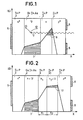
- FIG. 1 shows the structure of a photodiode with separate absorption and avalanche zones according to the known art.
- the geometry of such a photodiode is suitable for this, the representation of the diagram or profile of the electric field is superimposed on the representation of the structure by layers of semiconductors, on the drawing of the structure.
- this avalanche diode according to the known art is chosen in InP / GaInAs, the different layers of which are of type n and p.
- Such an avalanche photodiode is composed of an n + InP substrate marked 1: in reality, this layer 1 is composed of the substrate itself and of a buffer layer or buffer of the same material and of the same type of conductivity, the buffer layer being intended to smooth the relatively rough surface of the substrate.
- a layer 2 of GainAs of type n conductivity which will be called v because it is a n-doped zone n.
- v n-doped zone
- a layer 3 of n-type InP forms a heterojunction, with a large band gap, while the absorption layer is with a band gap.
- a contact layer 4 of InP of conductivity type p + ensures contact with the electrode metallization.
- Such a diode is supplemented by two metallizations of electrodes 5 on the side of the substrate and 6 on the side of the window through which the light detected by this avalanche diode penetrates.
- the contact metallizations, as well as the representation of the different layers making up the structure of such a photodiode, are very schematized.
- the surface region on the side of the contact point 6 constitutes a window which can act as a filter limiting towards the short wavelengths the spectrum of the light received by the device used as a photodetector.
- it constitutes a contact-making region and its location makes it possible to limit the absorption region of the device to the strictly useful area, for example the very small area corresponding to the section an optical fiber or a bundle of optical fibers.
- the electric field E in absolute value, developed by polarization, has been plotted on the vertical axis.
- This field is of little importance in the substrate, but in the absorption layer 2, it reaches a value of the order of 10 5 V / cm maximum, beyond which there would be a risk of breakdown the diode by tunnel effect. Then, in layer 3 with a large forbidden band, there is an elevation of the field, up to a maximum in which the avalanche occurs, while in layer 4 of contact making the field suddenly drops beyond the junction between layers 3 and 4, at a very low value.
- the photon detection and absorption zone is represented by zone 7, while the avalanche zone is represented at 8: the avalanche zone has a thickness of the order of 10 nm (100 ⁇ ).
- the brutal variaton of field in layer 3 can be considered as the case as an elevation of the field according to whether it is the holes which go from zone 2 towards zone 3 or as a lowering of the field if one consider the path of the photons: the fact remains that this field varies strongly as a function of the distance x and that consequently as has been said, there is statistically a high noise due to a brutal amplification by avalanche, this noise being d 'all the greater as the ratio of the ionization coefficients approaches unity, that is to say that the electric field is high.
- the noise is reduced while retaining a gain due to the high avalanche, the avalanche zone extending over a distance sufficient to obtain a gain under low electric field.
- FIG. 2 which gives the structure diagram of an avalanche diode according to the invention.
- Figure 2 is to be compared to Figure 1 in that it gives along the x-axis the various semiconductor layers which make up an avalanche photodiode and, superimposed along the y-axis, the curve of the electric field E in absolute value in these same layers.
- the application example of the invention described uses the compound III-V Ga x ln 1-x As, which makes it possible to cover the spectral range of 1 at 1.7 micrometer when it is adapted in crystalline mesh to an InP substrate.
- other materials can be used which fall within the scope of the invention.
- n 1 doped InP layer and of thickness x 1 such that n, is deposited.
- x 1 2.5 10 12 ionized impurity atoms per cm 2 .
- This field-lowering layer is marked 9 in FIG. 2 to differentiate it from layer 3 in FIG. 1.
- This layer 9 must meet the condition n 1 x 1 ⁇ 2.5 10 12 atoms / cm 2 .
- This layer 10 is, like layer 2, identified by the sign v, which indicates that it is not very doped.
- the pn electrical junction necessary to make a diode of this type is formed by implantation or diffusion in the layer of Inp 10 of a p-type dopant through an oxide mask, and to a depth such that l 'we have condition n 2 . x 2 ⁇ 1.3 10 12 at / cm 2 , X2 being the distance separating the junction of the interface between the two layers of InP 9 and 10.
- This implantation or diffusion operation therefore forms in layer 10 of type n 2 layer 11 of type p + shown in FIG. 2.
- the ohmic contacts are then produced by known means of metallization with a geometry allowing the transmission of light on at least one of the faces: in the figure shown, the ohmic contact 5 on the n + layer which is the substrate is not transparent to light and it is the ohmic contact 6 on the p + layer 11 which presents a window, for the passage of an optical fiber for example.
- the detection zone is, as in the diode of the prior art, zone 7 in the absorption layer 2.
- This detection zone corresponds to a maximum electric field of 10 5 volts / cm.
- the avalanche zone is marked 12 and corresponds to a minimum of 4.5 ⁇ 10 5 Volts / cm.
- This avalanche zone extends through the InP 10 avalanche layer, a layer in which the field varies little, but varies over a distance sufficient for the product of the amplification per unit of distance multiplied by the thickness of the layer gives a significant gain.
- the structure described is of the nvnvp type: however, if the materials used to make an avalanche photodiode are such that the ionization coefficient of the electrons is greater than that of the holes, it is then enough to make a structure of the pnpnn type to obtain a Avalanche photodiode with the same characteristics of high gain and low noise in excess of amplification. However, as a small excess noise is obtained for very different ionization coefficients, it is preferable to inject into the avalanche zone the carrier with the highest ionization coefficient, this is why the most general case is the case of an nvnvp diode.
- the invention has been explained by specifying, for the sole purpose of simplifying the explanations, that the materials are InP and GainAs: it has been said previously that other materials such as GaAISb, GaAIAsSb, GaSb for example are perfectly suitable.
- the structure of the diode has been exposed in its most general scheme, which corresponds to that of layers of semiconductor materials. None prevents this diode from being perfected by giving the various stated layers shapes which make it possible to optimize the diode according to the invention, which is specified by the claims below.
Landscapes
- Light Receiving Elements (AREA)
Applications Claiming Priority (2)
| Application Number | Priority Date | Filing Date | Title |
|---|---|---|---|
| FR8124164 | 1981-12-23 | ||
| FR8124164A FR2518817A1 (fr) | 1981-12-23 | 1981-12-23 | Photodiode a zones d'absorption et d'avalanche separees |
Publications (3)
| Publication Number | Publication Date |
|---|---|
| EP0082787A2 EP0082787A2 (fr) | 1983-06-29 |
| EP0082787A3 EP0082787A3 (en) | 1984-09-05 |
| EP0082787B1 true EP0082787B1 (fr) | 1987-06-10 |
Family
ID=9265362
Family Applications (1)
| Application Number | Title | Priority Date | Filing Date |
|---|---|---|---|
| EP82402340A Expired EP0082787B1 (fr) | 1981-12-23 | 1982-12-21 | Photodiode à zones d'absorption et d'avalanche séparées |
Country Status (5)
| Country | Link |
|---|---|
| EP (1) | EP0082787B1 (enExample) |
| JP (1) | JPS58114472A (enExample) |
| CA (1) | CA1180092A (enExample) |
| DE (1) | DE3276560D1 (enExample) |
| FR (1) | FR2518817A1 (enExample) |
Cited By (1)
| Publication number | Priority date | Publication date | Assignee | Title |
|---|---|---|---|---|
| US9379271B2 (en) | 2013-05-24 | 2016-06-28 | The United States Of America As Represented By The Secretary Of The Army | Variable range photodetector and method thereof |
Families Citing this family (6)
| Publication number | Priority date | Publication date | Assignee | Title |
|---|---|---|---|---|
| EP0150564A3 (en) * | 1983-10-26 | 1986-05-14 | AT&T Corp. | Electronic device comprising a heterojunction |
| JP3141080B2 (ja) * | 1994-06-22 | 2001-03-05 | ケイディディ株式会社 | 半導体機能素子 |
| US6720588B2 (en) | 2001-11-28 | 2004-04-13 | Optonics, Inc. | Avalanche photodiode for photon counting applications and method thereof |
| US8269222B2 (en) | 2010-05-25 | 2012-09-18 | The United States Of America As Represented By The Secretary Of The Army | Semiconductor photodetector with transparent interface charge control layer and method thereof |
| US8269223B2 (en) | 2010-05-27 | 2012-09-18 | The United States Of America As Represented By The Secretary Of The Army | Polarization enhanced avalanche photodetector and method thereof |
| US9893227B2 (en) | 2013-05-24 | 2018-02-13 | The United States Of America As Represented By The Secretary Of The Army | Enhanced deep ultraviolet photodetector and method thereof |
Citations (1)
| Publication number | Priority date | Publication date | Assignee | Title |
|---|---|---|---|---|
| GB2025693A (en) | 1978-07-17 | 1980-01-23 | Kokusai Denshin Denwa Co Ltd | Avalanche photo diode with semiconductor hetero structure |
Family Cites Families (2)
| Publication number | Priority date | Publication date | Assignee | Title |
|---|---|---|---|---|
| JPS52101990A (en) * | 1976-02-21 | 1977-08-26 | Hitachi Ltd | Semiconductor device for photoelectric transducer and its manufacture |
| JPS5793585A (en) * | 1980-12-02 | 1982-06-10 | Fujitsu Ltd | Semiconductor photoreceiving element |
-
1981
- 1981-12-23 FR FR8124164A patent/FR2518817A1/fr active Granted
-
1982
- 1982-12-20 CA CA000418122A patent/CA1180092A/en not_active Expired
- 1982-12-21 JP JP57224814A patent/JPS58114472A/ja active Pending
- 1982-12-21 DE DE8282402340T patent/DE3276560D1/de not_active Expired
- 1982-12-21 EP EP82402340A patent/EP0082787B1/fr not_active Expired
Patent Citations (1)
| Publication number | Priority date | Publication date | Assignee | Title |
|---|---|---|---|---|
| GB2025693A (en) | 1978-07-17 | 1980-01-23 | Kokusai Denshin Denwa Co Ltd | Avalanche photo diode with semiconductor hetero structure |
Non-Patent Citations (5)
| Title |
|---|
| "a high gain In Ga As/InP avalanche photodiode with no tunnelling leakage current", APPL. PHYS. LETT., vol. 39, no. 5, 1 September 1981 (1981-09-01), pages 402 - 404, XP055295562 |
| "ionization coeffecients of electrons and holes in InP", APPL. PHYS. LETT., vol. 35, no. 4, 15 August 1979 (1979-08-15), pages 333 - 335, XP055295562 |
| ANDO: "tunnelling current in InGaAs and optimum design for InGaAs/InP avalanche photodiode", JAPANESE JOURNAL OF APPLIED PHYSICS, vol. 19, no. 6, June 1980 (1980-06-01), pages L277 - L280, XP055295565 |
| PHILIPS TECHN. RDSCH., vol. 36, no. 7, 1976, pages 220 - 226, XP055295560 |
| S.M.SZE: "IMPATS and related transit time diodes", PHYSICS OF SEMICONDUCTOR DEVICES, 1981, USA, pages 568 - 579, XP055295566 |
Cited By (1)
| Publication number | Priority date | Publication date | Assignee | Title |
|---|---|---|---|---|
| US9379271B2 (en) | 2013-05-24 | 2016-06-28 | The United States Of America As Represented By The Secretary Of The Army | Variable range photodetector and method thereof |
Also Published As
| Publication number | Publication date |
|---|---|
| CA1180092A (en) | 1984-12-27 |
| FR2518817A1 (fr) | 1983-06-24 |
| EP0082787A3 (en) | 1984-09-05 |
| DE3276560D1 (en) | 1987-07-16 |
| EP0082787A2 (fr) | 1983-06-29 |
| JPS58114472A (ja) | 1983-07-07 |
| FR2518817B1 (enExample) | 1985-05-17 |
Similar Documents
| Publication | Publication Date | Title |
|---|---|---|
| EP0244299B1 (fr) | Photodiode PIN réalisée à partir de semiconducteur amorphe | |
| EP0545808B1 (fr) | Dispositif optoélectronique à très faible résistance série | |
| EP3084843B1 (fr) | Elément de détection quantique à faible bruit et procédé de fabrication d'un tel élément de photodétection | |
| US20170244002A1 (en) | AlInAsSb Avalanche Photodiode and Related Method thereof | |
| EP0236189B1 (fr) | Structure semi-conductrice monolithique d'un transistor bipolaire à hétérojonction et d'un laser | |
| JP3287458B2 (ja) | 超高速・低電圧駆動アバランシェ増倍型半導体受光素子 | |
| EP2359414B1 (fr) | Detecteur infrarouge a reponse spectrale etendue dans le visible | |
| EP1756872B1 (fr) | Circuit de detection photonique a structure mesa | |
| EP2865017B1 (fr) | Structure semiconductrice comportant une zone absorbante placée dans une cavité focalisante | |
| FR2492168A1 (fr) | Photodiode a semiconducteur | |
| EP0001728B1 (fr) | Diode émettrice et réceptrice de lumière notamment pour télécommunications optiques | |
| EP0082787B1 (fr) | Photodiode à zones d'absorption et d'avalanche séparées | |
| EP2750203B1 (fr) | Structure semiconductrice du type photodiode à avalanche à faible temps de réponse et procédé de fabrication d'une telle photodiode | |
| EP3353818A1 (fr) | Photodétecteur comprenant un empilement de couches superposées | |
| FR2758657A1 (fr) | Photodetecteur metal-semiconducteur-metal | |
| JPH038117B2 (enExample) | ||
| JPS60247979A (ja) | 半導体光素子 | |
| JP2751846B2 (ja) | 半導体受光素子 | |
| EP2382672B1 (fr) | Procédé de fabrication d'une photodiode et photodiode et détecteur de rayonnement electromagnétique correspondants | |
| FR2721439A1 (fr) | Eléments semi-conducteurs optiques et procédés de fabrication de ceux-ci. | |
| JPH0575160A (ja) | アバランシエホトダイオードおよびその動作方法 | |
| WO2025108863A1 (fr) | Photodiode sam à multiplication d'un seul type de porteurs dans une région à multicouche périodique | |
| JP2991555B2 (ja) | 半導体受光素子 | |
| JPH04263474A (ja) | 半導体受光素子の製造方法 | |
| EP0038733A2 (fr) | Photodiode de télécommunication à courant d'obscurité minimal |
Legal Events
| Date | Code | Title | Description |
|---|---|---|---|
| PUAI | Public reference made under article 153(3) epc to a published international application that has entered the european phase |
Free format text: ORIGINAL CODE: 0009012 |
|
| AK | Designated contracting states |
Designated state(s): DE GB NL |
|
| PUAL | Search report despatched |
Free format text: ORIGINAL CODE: 0009013 |
|
| AK | Designated contracting states |
Designated state(s): DE GB NL |
|
| 17P | Request for examination filed |
Effective date: 19840924 |
|
| GRAA | (expected) grant |
Free format text: ORIGINAL CODE: 0009210 |
|
| AK | Designated contracting states |
Kind code of ref document: B1 Designated state(s): DE GB NL |
|
| REF | Corresponds to: |
Ref document number: 3276560 Country of ref document: DE Date of ref document: 19870716 |
|
| PGFP | Annual fee paid to national office [announced via postgrant information from national office to epo] |
Ref country code: NL Payment date: 19871231 Year of fee payment: 6 |
|
| PLBI | Opposition filed |
Free format text: ORIGINAL CODE: 0009260 |
|
| 26 | Opposition filed |
Opponent name: STANDARD ELEKTRIK LORENZ AG Effective date: 19880309 |
|
| NLR1 | Nl: opposition has been filed with the epo |
Opponent name: STANDARD ELEKTRIK LORENZ AG |
|
| RAP4 | Party data changed (patent owner data changed or rights of a patent transferred) |
Owner name: THOMSON-CSF |
|
| RDAG | Patent revoked |
Free format text: ORIGINAL CODE: 0009271 |
|
| STAA | Information on the status of an ep patent application or granted ep patent |
Free format text: STATUS: PATENT REVOKED |
|
| 27W | Patent revoked |
Effective date: 19890612 |
|
| GBPR | Gb: patent revoked under art. 102 of the ep convention designating the uk as contracting state | ||
| NLR2 | Nl: decision of opposition |