EP0082065B1 - Dispositif de déclenchement d'un actionneur de sûreté - Google Patents
Dispositif de déclenchement d'un actionneur de sûreté Download PDFInfo
- Publication number
- EP0082065B1 EP0082065B1 EP82402234A EP82402234A EP0082065B1 EP 0082065 B1 EP0082065 B1 EP 0082065B1 EP 82402234 A EP82402234 A EP 82402234A EP 82402234 A EP82402234 A EP 82402234A EP 0082065 B1 EP0082065 B1 EP 0082065B1
- Authority
- EP
- European Patent Office
- Prior art keywords
- test
- turns
- triggering
- winding
- actuator
- Prior art date
- Legal status (The legal status is an assumption and is not a legal conclusion. Google has not performed a legal analysis and makes no representation as to the accuracy of the status listed.)
- Expired
Links
- 239000012190 activator Substances 0.000 title 1
- 238000004804 winding Methods 0.000 claims description 72
- 238000012360 testing method Methods 0.000 claims description 62
- 238000010586 diagram Methods 0.000 description 6
- 239000004065 semiconductor Substances 0.000 description 3
- 239000000758 substrate Substances 0.000 description 3
- 230000001681 protective effect Effects 0.000 description 2
- 230000001960 triggered effect Effects 0.000 description 2
- 230000004907 flux Effects 0.000 description 1
- 238000005259 measurement Methods 0.000 description 1
Images
Classifications
-
- G—PHYSICS
- G21—NUCLEAR PHYSICS; NUCLEAR ENGINEERING
- G21C—NUCLEAR REACTORS
- G21C17/00—Monitoring; Testing ; Maintaining
-
- H—ELECTRICITY
- H03—ELECTRONIC CIRCUITRY
- H03K—PULSE TECHNIQUE
- H03K19/00—Logic circuits, i.e. having at least two inputs acting on one output; Inverting circuits
- H03K19/02—Logic circuits, i.e. having at least two inputs acting on one output; Inverting circuits using specified components
- H03K19/16—Logic circuits, i.e. having at least two inputs acting on one output; Inverting circuits using specified components using saturable magnetic devices
-
- H—ELECTRICITY
- H03—ELECTRONIC CIRCUITRY
- H03K—PULSE TECHNIQUE
- H03K19/00—Logic circuits, i.e. having at least two inputs acting on one output; Inverting circuits
- H03K19/003—Modifications for increasing the reliability for protection
- H03K19/00392—Modifications for increasing the reliability for protection by circuit redundancy
-
- Y—GENERAL TAGGING OF NEW TECHNOLOGICAL DEVELOPMENTS; GENERAL TAGGING OF CROSS-SECTIONAL TECHNOLOGIES SPANNING OVER SEVERAL SECTIONS OF THE IPC; TECHNICAL SUBJECTS COVERED BY FORMER USPC CROSS-REFERENCE ART COLLECTIONS [XRACs] AND DIGESTS
- Y02—TECHNOLOGIES OR APPLICATIONS FOR MITIGATION OR ADAPTATION AGAINST CLIMATE CHANGE
- Y02E—REDUCTION OF GREENHOUSE GAS [GHG] EMISSIONS, RELATED TO ENERGY GENERATION, TRANSMISSION OR DISTRIBUTION
- Y02E30/00—Energy generation of nuclear origin
- Y02E30/30—Nuclear fission reactors
Definitions
- the present invention relates to a device for triggering a safety actuator. It applies in particular to the triggering of any safety actuator and to safety actuators which make it possible to trigger a protective action in a nuclear reactor.
- a nuclear reactor for example comprises a large number of devices which make it possible to control its operation. These devices are qualified as safety actuators. In the event of an incident, these actuators must be able to be triggered urgently, so that their protective action can stop this incident.
- the values of a certain number of physical quantities such as pressure, temperature, neutron flux, etc.
- the values of these quantities are then compared in different devices with reference values.
- These devices normally deliver logic comparison signals, of non-zero value, when the values of the physical quantities are situated in a range of values defined in advance, corresponding to the normal operation of the reactor. When the physical quantities leave this safety range, these devices deliver logic output signals, of zero values for example.
- these triggering devices are 2/2 type logic devices which make it possible to trigger an urgent action by a signal supplied on an output, this signal having, for example, logic state 1, when two of its inputs receive control signals whose logic state is 0; these control signals come from the devices mentioned above.
- Safety actuator triggering devices comprising triggering means constituted, for example, by an OR gate with inverted output, two of the inputs of this gate being respectively connected to the outputs of two AND gates with two inputs.
- triggering means constituted, for example, by an OR gate with inverted output, two of the inputs of this gate being respectively connected to the outputs of two AND gates with two inputs.
- These doors each receive, on one of their control inputs, a control signal from the devices mentioned above, while another input can receive a test signal which makes it possible to impose, at the output of the door OR, a predetermined logic state signal 1, whatever the logic state of the control signals applied to each of the control inputs of the two AND gates.
- the object of the present invention is to remedy these drawbacks and in particular to produce a device for triggering a safety actuator having a higher output power than that which can be obtained using devices comprising integrated circuits.
- the subject of the invention is a device for triggering a safety actuator comprising triggering means, one output of which provides an output signal which may have two logic states, one of these states corresponding to the triggering of the actuator, and the other state corresponding to the absence of triggering of the latter, means for testing and controlling these triggering means, these test and control means comprising two control inputs receiving signals for controlling the triggering means so that the output signal has one of the two logic states, and a test input receiving a test signal so that said output provides an output signal whose logic state corresponds to the triggering of the actuator even if the signals control cause the supply of an output signal corresponding to the absence of tripping, characterized in that the test and control means consist of three primary windings of a magnetic amplifier, two of these primary windings receiving direct currents corresponding to the control signals, another of these windings being a test winding receiving a direct current corresponding to the test signal, the tripping means being constituted by a winding secondary of the magnetic amplifier, this secondary winding being connected to an
- the numbers of ampere-turns of the windings are chosen so that, when the numbers of ampere-turns of the primary windings are zero, the average intensity of the current corresponding to the signal of output applied to the trigger is maximum and corresponds to the logic state of triggering of the actuator, this intensity being less than a predetermined threshold and corresponding to the logic state of no triggering of the actuator when the numbers of amps -tours of the control windings are both, or one or the other, greater than a predetermined value while the number of ampere-turns of the test winding is zero, this intensity being maximum and corresponding to the actuator trip logic state when the number of ampere-turns of the control windings are both, or both, greater than a predetermined value while the number of ampere-turns of the' test winding is greater than a predetermined value.
- the number of turns of the test winding is twice the number of turns of each control winding, the intensities of the circulating currents in the control windings and in the test winding being equal when the number of ampere-turns of these windings is greater than the predetermined values, the direction of the current in the test winding being opposite to the direction of the currents in each winding control.
- the voltage source is a sinusoidal voltage source, the rectifier bridge being a full-wave rectifier bridge.
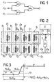
- Fig. 1 schematically represents a device for triggering a safety actuator, known in the state of the art and consisting of low power logic circuits, of the type integrated on a semiconductor substrate.
- This device comprises triggering means, constituted by a gate OU1 of which an output S provides an output signal which can have two logic states 0 or 1; one of these states (logic state 1 for example) corresponds to the triggering of a safety actuator receiving the signal supplied by output S and the other state (0 for example) corresponds to the absence of triggering of this actuator.
- This device also comprises means for testing and controlling the triggering means; these test and control means are constituted here by the logic gates ET1 and ET2.
- These doors include control inputs E1 and E2 which respectively receive control signals from the triggering means (gate OU1); these control signals come from the devices described above and which make it possible to compare, with reference values, the parameter values supplied by measurement sensors.
- the second inputs of these doors (referenced E3) are test inputs which receive a test signal.
- the logic state of this test signal is such that, whatever the logic states of the control signals applied to the inputs E1 and E2, the output S of the device provides a signal whose logic state (1 for example) corresponds when the actuator trips.
- the test inputs of the gates ET1 and ET2 are inverted inputs, while the output of the OR gate is an inverted output.
- the logic table below represents the logic states of the signals at different points of the device and allows a better understanding of how it works:
- logic state 0 represents an absence of information or voltage
- logic state 1 represents a presence of information or voltage. Note in this table that, when the test input E3 receives a signal of logic level 0, the output S of the device remains in logic state 0 as long as the two control inputs E1 and E2, or one at less than these two inputs, receive signals in logic state 1.
- the fifth, sixth and seventh lines of the table show that, in the case where the test input E3 receives a test signal having the logic state 1, the output S of the device remains in the logic state 1, even if the two control inputs E1 and E2 or at least one of these inputs receives a signal which is in logic state 1. It follows that the application of a test signal in logic state 1 on l the test input E3 of the device causes the appearance of a signal for triggering a logic state 1, on the output of the device, regardless of the logic state of the control signals applied to the inputs E1 and E2.
- Fig. 2 schematically represents a device for triggering a safety actuator, according to the invention, the operation of which corresponds to the preceding logic table.
- This device which will be described later in detail, comprises triggering means and means for controlling and testing these triggering means; the test means making it possible, when they receive a predetermined logic state test signal, to control the triggering means so that the latter provide on their output a signal corresponding to the triggering of a safety actuator.
- This trigger signal appears even if the control signals applied to the control means normally correspond to the absence of actuator triggering.
- the test means and control applied to the control means normally correspond to the absence of tripping of the actuator.
- test and control means as well as the triggering means are parts of a magnetic amplifier constituted by two identical toroidal transformers T1 and T2, with rectangular hysteresis cycle.
- Two of the primary windings P1 of each of these transformers, connected in series form a winding P 1 receiving control signals on its input E 1 .
- two other primary windings connected in series with each of these transformers form a winding P2 receiving control signals on its input E2; these signals correspond to currents IC1, IC2.
- a third primary winding P3 of the transformer is a test winding which receives, on an input E3, a test current IC3 corresponding to the test signal described above. This current can be supplied by an electric current source, not shown.
- the triggering means are constituted by the secondary winding Pi of the magnetic amplifier which here comprises the two identical windings of the secondary of the transformers T1 and T2. denotes in this figure the number of turns of each secondary winding of the transformers T1 and T2.
- the secondary winding of the magnetic amplifier is connected to a source V of sinusoidal alternating voltage. This source is connected between the common point P of the secondary transformers T1 and T2 and one of the terminals of a rectifier bridge comprising the diodes D1, D2, D3, D4, in the diagonal of which is connected the safety actuator shown schematically in D.
- the reference I designates the average value of the rectified current, while C 1 and C 2 represent the magnetic carcasses of the transformers T1 and T2.
- the directions of the currents in the windings are indicated by arrows in the figure.
- the direction of current IC3 in the test winding is opposite to the directions of current IC1 and IC2 in the control windings.
- FIG. 3 provides a better understanding of the operation of the device of the invention.
- This figure is a transfer diagram which represents the variations of the average value of the rectified current I in the actuator D, according to the sum of the numbers of ampere-turns-N1IC1-N2IC2-N3lC3 of the primary windings of the amplifier magnetic (IC1, IC2, IC3 being positive). It is assumed, in a preferred embodiment, that the number of ampere-turns in the secondary winding of the amplifier, which corresponds to the product of the number Ni of turns of this winding with the mean value of the current intensity rectified I in the actuator D, is equal to the algebraic sum of the ampere-turns of the primary windings.
- the numbers of ampere-turns are chosen so that, when the numbers of ampere-turns N1IC1, N2IC2, N3IC3 are zero (the intensities of the currents IC1, IC2, IC3 being zero), the value of the intensity of the average current I in the actuator, that is to say at the output S of the triggering means, is maximum.
- This maximum intensity corresponds to the appearance of an actuator trigger signal, having logic state 1, while the zero values of the intensities of the currents IC1, IC2, IC3 in each primary control and test winding correspond to logic states 0.
- This case in fact corresponds to the fourth line of the logic table described above and to the triggering of the actuator by the control signals.
- the operating point on the transfer diagram in fig. 3 is located in C.
- the value of the average intensity of the rectified current 1 flowing in the actuator D is less than a predetermined threshold IS, when the numbers of ampere-turns N1 IC1, N21C2 of the control windings (inputs E1 and E2) are all two, or either, greater than a predetermined value when the number of ampere-turns N31C3 (input E3) of the test winding is zero.
- a predetermined threshold IS when the numbers of ampere-turns N1 IC1, N21C2 of the control windings (inputs E1 and E2) are all two, or either, greater than a predetermined value when the number of ampere-turns N31C3 (input E3) of the test winding is zero.
- the intensity of the current IC3 in the test winding being zero, this corresponds to a logic state test signal 0, applied to the test winding; the intensities of the currents IC1 and IC2 are such that the numbers of ampere-turns N1 IC1, N2, IC2 in the two control windings are both, or one or the other, greater than a predetermined value, this means for example that if only the number of ampere-turns N1IC1 is greater than the predetermined value, while the numbers of ampere-turns N21C2, N31C3 are equal to 0, the operating point is located at B on the diagram of fig. 3, the intensity of the current I in the actuator is less than the threshold IS; this case corresponds to the third line of the logic table described above, the logic state of the signal on the output S being considered to be logic state 0.
- the operating point is located at A in fig. 3.
- the value of the rectified average current in the actuator D is lower than the threshold IS and this case also corresponds to a signal having the logic state 0 on the output S of the device (first line of the logic table described above).
- the operating point is located at C, F or G on the transfer diagram.
- the value of the rectified average current in the actuator D is maximum. This value corresponds to the application of a logic state 1 to the input of the actuator D. This logic state is maintained whatever the values N1 IC1, N21C2 of the numbers of ampere-turns of the control windings. If the numbers of ampere-turns N11C1, N21C2 are less than a predetermined value, the signals applied to the inputs E1 and E2 can be considered to have logic state 0; the operating point is located in G on the transfer diagram.
- the logic state of the signal on the output S is 1. If, on the contrary, the numbers of ampere-turns N1.IC1, N2! C2 are greater than a predetermined value, the signals applied to the inputs E1 and E2 of the device are considered as logic status signals 1, which corresponds to the seventh row of the logic table.
- the logic state of the signal on output S is 1.
- the operating point is C.
- the device which has just been described makes it possible to trigger a safety actuator requiring a triggering power greater than that which can be supplied by conventional logic circuits. It also makes it possible to verify that, whatever the control signals supplied to it and thanks to test signals applied to it, the actuator can be triggered by a signal whose logic state corresponds to this triggering. Finally, thanks to this device, the tests are "transparent". Indeed, whatever the test signal applied to the test input E3, the safety action (actuator triggering) can be implemented by applying signals triggering this action, on the inputs E1, E2 .
Landscapes
- Physics & Mathematics (AREA)
- Engineering & Computer Science (AREA)
- General Engineering & Computer Science (AREA)
- Computer Hardware Design (AREA)
- Computing Systems (AREA)
- Mathematical Physics (AREA)
- Plasma & Fusion (AREA)
- High Energy & Nuclear Physics (AREA)
- Tests Of Electronic Circuits (AREA)
- Safety Devices In Control Systems (AREA)
- Testing Electric Properties And Detecting Electric Faults (AREA)
- Control Of Electric Motors In General (AREA)
- Monitoring And Testing Of Nuclear Reactors (AREA)
- Testing And Monitoring For Control Systems (AREA)
Applications Claiming Priority (2)
| Application Number | Priority Date | Filing Date | Title |
|---|---|---|---|
| FR8123203A FR2518288A1 (fr) | 1981-12-11 | 1981-12-11 | Dispositif de declenchement d'un actionneur de surete |
| FR8123203 | 1981-12-11 |
Publications (2)
| Publication Number | Publication Date |
|---|---|
| EP0082065A1 EP0082065A1 (fr) | 1983-06-22 |
| EP0082065B1 true EP0082065B1 (fr) | 1985-07-24 |
Family
ID=9264928
Family Applications (1)
| Application Number | Title | Priority Date | Filing Date |
|---|---|---|---|
| EP82402234A Expired EP0082065B1 (fr) | 1981-12-11 | 1982-12-07 | Dispositif de déclenchement d'un actionneur de sûreté |
Country Status (7)
| Country | Link |
|---|---|
| US (1) | US4587077A (enExample) |
| EP (1) | EP0082065B1 (enExample) |
| JP (2) | JPS58149501A (enExample) |
| KR (1) | KR900009066B1 (enExample) |
| DE (1) | DE3264946D1 (enExample) |
| FR (1) | FR2518288A1 (enExample) |
| ZA (1) | ZA829069B (enExample) |
Families Citing this family (4)
| Publication number | Priority date | Publication date | Assignee | Title |
|---|---|---|---|---|
| US4696785A (en) * | 1985-10-31 | 1987-09-29 | Westinghouse Electric Corp. | Testable voted logic power circuit and method of testing the same |
| US4683105A (en) * | 1985-10-31 | 1987-07-28 | Westinghouse Electric Corp. | Testable, fault-tolerant power interface circuit for normally de-energized loads |
| US5442303A (en) * | 1992-07-16 | 1995-08-15 | The Nippon Signal Co., Ltd. | Electromagnetically coupled fail-safe logic circuit |
| US10755825B2 (en) * | 2018-10-31 | 2020-08-25 | Ge-Hitachi Nuclear Energy Americas Llc | Passive electrical component for safety system shutdown using Faraday's law |
Family Cites Families (10)
| Publication number | Priority date | Publication date | Assignee | Title |
|---|---|---|---|---|
| GB838809A (en) * | 1958-10-17 | 1960-06-22 | Standard Telephones Cables Ltd | Improvements in or relating to magnetic switching circuits |
| GB901215A (en) * | 1960-02-25 | 1962-07-18 | Standard Telephones Cables Ltd | Improvements in or relating to a fail safe electrical circuit |
| US3424652A (en) * | 1966-04-26 | 1969-01-28 | Kernforschung Gmbh Ges Fuer | Method and device for the supervision of installations,in particular safety switching system of nuclear reactors |
| US3437556A (en) * | 1967-10-23 | 1969-04-08 | Combustion Eng | Test circuit for reactor safety control system |
| GB1336296A (en) * | 1970-12-02 | 1973-11-07 | Molekularelektronik | Integrated circuit arrangments |
| US3855590A (en) * | 1972-04-04 | 1974-12-17 | Westinghouse Electric Corp | Cyclic or monitoring system for displaying the output of two substantially similar trains of logic |
| FR2294473A1 (fr) * | 1974-12-11 | 1976-07-09 | Commissariat Energie Atomique | Procede et dispositif electronique de commande a securite positive |
| GB1546587A (en) * | 1974-12-11 | 1979-05-23 | Commissariat Energie Atomique | Positive-safety units haveing the functions of control relay and current regulation |
| US4308099A (en) * | 1979-01-22 | 1981-12-29 | The Babcock & Wilcox Company | Nuclear reactor safety system |
| US4434132A (en) * | 1981-04-09 | 1984-02-28 | Westinghouse Electric Corp. | Power supply with nuclear reactor |
-
1981
- 1981-12-11 FR FR8123203A patent/FR2518288A1/fr active Granted
-
1982
- 1982-12-07 EP EP82402234A patent/EP0082065B1/fr not_active Expired
- 1982-12-07 DE DE8282402234T patent/DE3264946D1/de not_active Expired
- 1982-12-09 ZA ZA829069A patent/ZA829069B/xx unknown
- 1982-12-10 US US06/448,626 patent/US4587077A/en not_active Expired - Fee Related
- 1982-12-10 JP JP57216763A patent/JPS58149501A/ja active Pending
- 1982-12-11 KR KR8205554A patent/KR900009066B1/ko not_active Expired
-
1991
- 1991-04-19 JP JP026935U patent/JPH0587599U/ja active Pending
Also Published As
| Publication number | Publication date |
|---|---|
| FR2518288B1 (enExample) | 1984-04-06 |
| DE3264946D1 (en) | 1985-08-29 |
| JPS58149501A (ja) | 1983-09-05 |
| KR840003091A (ko) | 1984-08-13 |
| US4587077A (en) | 1986-05-06 |
| ZA829069B (en) | 1983-10-26 |
| JPH0587599U (ja) | 1993-11-26 |
| KR900009066B1 (ko) | 1990-12-20 |
| EP0082065A1 (fr) | 1983-06-22 |
| FR2518288A1 (fr) | 1983-06-17 |
Similar Documents
| Publication | Publication Date | Title |
|---|---|---|
| EP0037751B1 (fr) | Déclencheur statique perfectionné pour disjoncteur électrique | |
| EP1890165B1 (fr) | Procédé de détection directionnel d'un défaut à la terre et dispositif pour sa mise en oeuvre | |
| EP0454597A1 (fr) | Circuit de commande de grille par impulsion avec securité de court-circuit | |
| EP0082065B1 (fr) | Dispositif de déclenchement d'un actionneur de sûreté | |
| EP3015870B1 (fr) | Dispositif de mesure d'un courant hache | |
| FR2772923A1 (fr) | Circuit electronique de surveillance de tension electrique | |
| EP0354841B1 (fr) | Dispositif de surveillance du deséquilibre de la puissance électrique appelée sur les lignes conductrices d'un réseau électrique alternatif ou d'une installation intérieure triphasé | |
| FR3101428A1 (fr) | Disjoncteur et appareil mobile | |
| EP0592337B2 (fr) | Déclencheur électronique comportant une protection terre | |
| EP0605335B1 (fr) | Déclencheur électronique comportant un dispositif de test | |
| EP1166134B1 (fr) | Procede de surveillance de la circulation d'un courant sensiblement continu dans une charge | |
| EP0115994A1 (fr) | Interface pour relier un système informatique à un dispositif actionneur | |
| EP0053082B1 (fr) | Système logique de sécurité pour déclencher l'action de protection d'un actionneur de sûreté | |
| EP4241353B1 (fr) | Dispositifs de surveillance et de protection de circuits de puissance | |
| WO2000063932A1 (fr) | Systeme de diagnostic de contact electrique a deplacement mecanique | |
| EP0562959B1 (fr) | Module d'entrée d'information par contact électrique pour installation de contrÔle/commande | |
| FR2522824A1 (fr) | Dispositif pour appliquer des signaux logiques de test a deux etats sur une entree d'un circuit logique et application aux tests automatiques d'une pluralite de circuits logiques | |
| EP4632778A1 (fr) | Dispositif de protection électrique, installation électrique et procédé de commande associés | |
| EP3664240A1 (fr) | Dispositif de détection de court-circuit dans un bras de commutation | |
| FR3042878A1 (fr) | Chaine de mesure pour un circuit electronique de signalisation | |
| FR2827676A1 (fr) | Procede de diagnostic d'etage de puissance discret par des entrees numeriques | |
| EP4546588A1 (fr) | Dispositif de protection électrique différentielle | |
| EP0619561A1 (fr) | Circuit d'interface ayant deux bornes d'entrée et permettant conjointement d'alimenter un circuit d'application et de communiquer avec ce dernier | |
| FR2884660A1 (fr) | Agencement de circuit electronique pour la commutation d'une charge electrique d'une maniere sure en cas de defaillance | |
| EP0540379A1 (fr) | Disjoncteur différentiel centralisé |
Legal Events
| Date | Code | Title | Description |
|---|---|---|---|
| PUAI | Public reference made under article 153(3) epc to a published international application that has entered the european phase |
Free format text: ORIGINAL CODE: 0009012 |
|
| AK | Designated contracting states |
Designated state(s): BE DE FR GB IT |
|
| 17P | Request for examination filed |
Effective date: 19831129 |
|
| ITF | It: translation for a ep patent filed | ||
| GRAA | (expected) grant |
Free format text: ORIGINAL CODE: 0009210 |
|
| AK | Designated contracting states |
Designated state(s): BE DE FR GB IT |
|
| REF | Corresponds to: |
Ref document number: 3264946 Country of ref document: DE Date of ref document: 19850829 |
|
| PLBE | No opposition filed within time limit |
Free format text: ORIGINAL CODE: 0009261 |
|
| STAA | Information on the status of an ep patent application or granted ep patent |
Free format text: STATUS: NO OPPOSITION FILED WITHIN TIME LIMIT |
|
| 26N | No opposition filed | ||
| ITTA | It: last paid annual fee | ||
| PGFP | Annual fee paid to national office [announced via postgrant information from national office to epo] |
Ref country code: GB Payment date: 19941205 Year of fee payment: 13 Ref country code: BE Payment date: 19941205 Year of fee payment: 13 |
|
| PGFP | Annual fee paid to national office [announced via postgrant information from national office to epo] |
Ref country code: DE Payment date: 19941209 Year of fee payment: 13 |
|
| PG25 | Lapsed in a contracting state [announced via postgrant information from national office to epo] |
Ref country code: GB Effective date: 19951207 |
|
| PG25 | Lapsed in a contracting state [announced via postgrant information from national office to epo] |
Ref country code: BE Effective date: 19951231 |
|
| BERE | Be: lapsed |
Owner name: FRAMATOME ET CIE Effective date: 19951231 Owner name: COMMISSARIAT A L'ENERGIE ATOMIQUE ETABLISSEMENT D Effective date: 19951231 |
|
| GBPC | Gb: european patent ceased through non-payment of renewal fee |
Effective date: 19951207 |
|
| PG25 | Lapsed in a contracting state [announced via postgrant information from national office to epo] |
Ref country code: DE Effective date: 19960903 |
|
| PGFP | Annual fee paid to national office [announced via postgrant information from national office to epo] |
Ref country code: FR Payment date: 19981229 Year of fee payment: 17 |
|
| PG25 | Lapsed in a contracting state [announced via postgrant information from national office to epo] |
Ref country code: FR Free format text: LAPSE BECAUSE OF NON-PAYMENT OF DUE FEES Effective date: 20000831 |
|
| REG | Reference to a national code |
Ref country code: FR Ref legal event code: ST |