EP0080652A2 - Phototransistor in MOS thin-film technology, method of manufacturing it and method of using it - Google Patents
Phototransistor in MOS thin-film technology, method of manufacturing it and method of using it Download PDFInfo
- Publication number
- EP0080652A2 EP0080652A2 EP82110602A EP82110602A EP0080652A2 EP 0080652 A2 EP0080652 A2 EP 0080652A2 EP 82110602 A EP82110602 A EP 82110602A EP 82110602 A EP82110602 A EP 82110602A EP 0080652 A2 EP0080652 A2 EP 0080652A2
- Authority
- EP
- European Patent Office
- Prior art keywords
- layer
- polycrystalline silicon
- source
- silicon
- semiconductor body
- Prior art date
- Legal status (The legal status is an assumption and is not a legal conclusion. Google has not performed a legal analysis and makes no representation as to the accuracy of the status listed.)
- Granted
Links
- 238000004519 manufacturing process Methods 0.000 title claims abstract description 8
- 239000010409 thin film Substances 0.000 title claims abstract description 7
- 238000005516 engineering process Methods 0.000 title claims abstract description 6
- 238000000034 method Methods 0.000 title claims description 7
- 229910021420 polycrystalline silicon Inorganic materials 0.000 claims abstract description 25
- 239000004065 semiconductor Substances 0.000 claims abstract description 19
- 230000003647 oxidation Effects 0.000 claims abstract description 11
- 238000007254 oxidation reaction Methods 0.000 claims abstract description 11
- 238000000151 deposition Methods 0.000 claims description 10
- 239000000758 substrate Substances 0.000 claims description 10
- 238000002161 passivation Methods 0.000 claims description 9
- 229910004298 SiO 2 Inorganic materials 0.000 claims description 8
- XUIMIQQOPSSXEZ-UHFFFAOYSA-N Silicon Chemical compound [Si] XUIMIQQOPSSXEZ-UHFFFAOYSA-N 0.000 claims description 8
- 230000008021 deposition Effects 0.000 claims description 8
- 229910052710 silicon Inorganic materials 0.000 claims description 8
- 229910021417 amorphous silicon Inorganic materials 0.000 claims description 7
- 229910052581 Si3N4 Inorganic materials 0.000 claims description 6
- 239000010703 silicon Substances 0.000 claims description 6
- HQVNEWCFYHHQES-UHFFFAOYSA-N silicon nitride Chemical compound N12[Si]34N5[Si]62N3[Si]51N64 HQVNEWCFYHHQES-UHFFFAOYSA-N 0.000 claims description 6
- 239000012808 vapor phase Substances 0.000 claims description 6
- 229910052785 arsenic Inorganic materials 0.000 claims description 5
- 238000009792 diffusion process Methods 0.000 claims description 5
- 238000005468 ion implantation Methods 0.000 claims description 5
- 239000000463 material Substances 0.000 claims description 4
- UFHFLCQGNIYNRP-UHFFFAOYSA-N Hydrogen Chemical compound [H][H] UFHFLCQGNIYNRP-UHFFFAOYSA-N 0.000 claims description 3
- BLRPTPMANUNPDV-UHFFFAOYSA-N Silane Chemical group [SiH4] BLRPTPMANUNPDV-UHFFFAOYSA-N 0.000 claims description 3
- -1 arsenic ions Chemical class 0.000 claims description 3
- 229910052739 hydrogen Inorganic materials 0.000 claims description 3
- 239000001257 hydrogen Substances 0.000 claims description 3
- 229910000077 silane Inorganic materials 0.000 claims description 3
- 238000005979 thermal decomposition reaction Methods 0.000 claims description 3
- RQNWIZPPADIBDY-UHFFFAOYSA-N arsenic atom Chemical compound [As] RQNWIZPPADIBDY-UHFFFAOYSA-N 0.000 claims description 2
- 239000010410 layer Substances 0.000 claims 23
- 229910021419 crystalline silicon Inorganic materials 0.000 claims 2
- 239000011241 protective layer Substances 0.000 claims 2
- 239000002019 doping agent Substances 0.000 claims 1
- 229910052751 metal Inorganic materials 0.000 claims 1
- 239000002184 metal Substances 0.000 claims 1
- 238000007740 vapor deposition Methods 0.000 claims 1
- VYPSYNLAJGMNEJ-UHFFFAOYSA-N Silicium dioxide Chemical compound O=[Si]=O VYPSYNLAJGMNEJ-UHFFFAOYSA-N 0.000 abstract description 3
- 229910052681 coesite Inorganic materials 0.000 abstract description 2
- 229910052906 cristobalite Inorganic materials 0.000 abstract description 2
- 229910052682 stishovite Inorganic materials 0.000 abstract description 2
- 229910052905 tridymite Inorganic materials 0.000 abstract description 2
- 239000000377 silicon dioxide Substances 0.000 abstract 1
- 235000012239 silicon dioxide Nutrition 0.000 abstract 1
- 230000007547 defect Effects 0.000 description 6
- WUPHOULIZUERAE-UHFFFAOYSA-N 3-(oxolan-2-yl)propanoic acid Chemical compound OC(=O)CCC1CCCO1 WUPHOULIZUERAE-UHFFFAOYSA-N 0.000 description 3
- 229910052980 cadmium sulfide Inorganic materials 0.000 description 3
- 230000000694 effects Effects 0.000 description 2
- 238000009413 insulation Methods 0.000 description 2
- LIVNPJMFVYWSIS-UHFFFAOYSA-N silicon monoxide Chemical compound [Si-]#[O+] LIVNPJMFVYWSIS-UHFFFAOYSA-N 0.000 description 2
- 238000000137 annealing Methods 0.000 description 1
- 230000004888 barrier function Effects 0.000 description 1
- WUKWITHWXAAZEY-UHFFFAOYSA-L calcium difluoride Chemical compound [F-].[F-].[Ca+2] WUKWITHWXAAZEY-UHFFFAOYSA-L 0.000 description 1
- 229910001634 calcium fluoride Inorganic materials 0.000 description 1
- 239000000969 carrier Substances 0.000 description 1
- 238000006243 chemical reaction Methods 0.000 description 1
- 238000005229 chemical vapour deposition Methods 0.000 description 1
- 238000010276 construction Methods 0.000 description 1
- 238000002347 injection Methods 0.000 description 1
- 239000007924 injection Substances 0.000 description 1
- 229910021421 monocrystalline silicon Inorganic materials 0.000 description 1
- 238000011017 operating method Methods 0.000 description 1
- 231100000289 photo-effect Toxicity 0.000 description 1
- 230000001681 protective effect Effects 0.000 description 1
Images
Classifications
-
- H—ELECTRICITY
- H01—ELECTRIC ELEMENTS
- H01L—SEMICONDUCTOR DEVICES NOT COVERED BY CLASS H10
- H01L29/00—Semiconductor devices specially adapted for rectifying, amplifying, oscillating or switching and having potential barriers; Capacitors or resistors having potential barriers, e.g. a PN-junction depletion layer or carrier concentration layer; Details of semiconductor bodies or of electrodes thereof ; Multistep manufacturing processes therefor
- H01L29/02—Semiconductor bodies ; Multistep manufacturing processes therefor
- H01L29/04—Semiconductor bodies ; Multistep manufacturing processes therefor characterised by their crystalline structure, e.g. polycrystalline, cubic or particular orientation of crystalline planes
-
- H—ELECTRICITY
- H01—ELECTRIC ELEMENTS
- H01L—SEMICONDUCTOR DEVICES NOT COVERED BY CLASS H10
- H01L31/00—Semiconductor devices sensitive to infrared radiation, light, electromagnetic radiation of shorter wavelength or corpuscular radiation and specially adapted either for the conversion of the energy of such radiation into electrical energy or for the control of electrical energy by such radiation; Processes or apparatus specially adapted for the manufacture or treatment thereof or of parts thereof; Details thereof
- H01L31/08—Semiconductor devices sensitive to infrared radiation, light, electromagnetic radiation of shorter wavelength or corpuscular radiation and specially adapted either for the conversion of the energy of such radiation into electrical energy or for the control of electrical energy by such radiation; Processes or apparatus specially adapted for the manufacture or treatment thereof or of parts thereof; Details thereof in which radiation controls flow of current through the device, e.g. photoresistors
- H01L31/10—Semiconductor devices sensitive to infrared radiation, light, electromagnetic radiation of shorter wavelength or corpuscular radiation and specially adapted either for the conversion of the energy of such radiation into electrical energy or for the control of electrical energy by such radiation; Processes or apparatus specially adapted for the manufacture or treatment thereof or of parts thereof; Details thereof in which radiation controls flow of current through the device, e.g. photoresistors characterised by potential barriers, e.g. phototransistors
- H01L31/101—Devices sensitive to infrared, visible or ultraviolet radiation
- H01L31/112—Devices sensitive to infrared, visible or ultraviolet radiation characterised by field-effect operation, e.g. junction field-effect phototransistor
- H01L31/113—Devices sensitive to infrared, visible or ultraviolet radiation characterised by field-effect operation, e.g. junction field-effect phototransistor being of the conductor-insulator-semiconductor type, e.g. metal-insulator-semiconductor field-effect transistor
- H01L31/1136—Devices sensitive to infrared, visible or ultraviolet radiation characterised by field-effect operation, e.g. junction field-effect phototransistor being of the conductor-insulator-semiconductor type, e.g. metal-insulator-semiconductor field-effect transistor the device being a metal-insulator-semiconductor field-effect transistor
Definitions
- the invention relates to a phototransistor using MOS thin-film technology, a method for its production and a method for its operation.
- Phototransistors are mainly bipolar transistors in which the emitter-collector current is increased by photo-injection of minority carriers into the base.
- a big disadvantage of these phototransistors is the upper frequency limit at a few kHz.
- the structure of such a transistor can be found, for example, in volume 2, semiconductor electronics, R. Müller “Components of semiconductor electronics", 2nd edition, on page 124.
- a photo transistor in MOS thin-film technology is from "Physics of thin films” Vo. 2, G.-Hass and RE Thun, Academic Press (1964) from an essay by PK Weimer "The Insulated-Gate Thin Film Transistor” on page 187.
- the light-sensitive transistor described here consists of photoconductive cadmium sulfide (CdS) and contains an insulation layer made of silicon monoxide or calcium fluoride, which is additionally vapor-deposited onto the cadmium sulfide layer. Deep and flat volume traps serve to explain the photo effect. The flat traps under the conduction band are additionally occupied by light and then emptied by field ionization. This increases the drain current through the photo current.
- This transistor is already conducting in the dark and has poor transistor properties (distorted characteristics). Since the semiconductor body consists of a connection and the insulation layer too must also be applied, its production is difficult to reproduce.
- the object on which the invention is based is to create a phototransistor which is not only easy to manufacture and can be arranged in a space-saving manner in a second semiconductor plane, but also has the property of only conducting when exposed as a function of light intensity and operating frequency to change.
- the transistor should also be applicable at high frequencies (f >> 10 kHz) and small operating voltages of 5 - 10 V.
- the interface between the polycrystalline silicon and the oxide generated by thermal oxidation has a high defect density in the vicinity of the conduction band.
- defects in the volume of the polycrystalline silicon or grain boundaries mean that in the unexposed state when an AC voltage (1 kHz) is applied to the gate, no electron current flows from the source to the drain.
- the surface potential can follow the gate voltage very slowly. Many interface defects or grain boundaries have to be reloaded. This effect affects the transistor properties such as high threshold voltage and small mobility. During exposure, the interfaces and volume defects are now partially filled, and with increasing exposure intensity, more and more defects are already occupied or the grain boundary barriers are broken down and the surface potential and thus the drain current follow the gate voltage more quickly. For the transistor properties, this means that the threshold voltage drops, while the mobility of the electrons increases. An electron current can now flow from source to drain as a function of the gate voltage. The conductance of the transistor increases with the light intensity. At high light intensities, frequencies of> 10 kHz can be achieved. This is a new type of photo transistor effect.
- the polycrystalline silicon semiconductor body is produced by deposition from the vapor phase on a low-resistance, single-crystal silicon substrate which acts as a gate electrode and is provided by oxidation with an SiO 2 layer, or by deposition from the vapor phase on an insulating substrate and that the source and drain zones in polycrystalline silicon semiconductor bodies with a concentration of greater than 10 19 arsenic cm -3 are doped by masked diffusion or ion implantation.
- the phototransistor with a passivation layer made of a material containing silicon and hydrogen in order to reduce the density of the fast surface states. This measure ensures that the free valences at the Si / Si02 interface are offset with hydrogen be satisfied.
- Suitable material is silicon nitride or amorphous silicon, which is generated by an electrical low-pressure glow discharge.
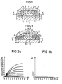
- Figures 1 and 2 show schematically in the sectional view two special embodiments, Figures 3a and 3b the transistor characteristics (100-1000 Hz) without exposure (3b) and with exposure (3a).
- an SiO 2 layer 2 of 30 to 50 nm thickness is produced on a single-crystalline, low-resistance ( ⁇ 0.1 ohm / cm) silicon substrate 1 by thermal oxidation and then at 625 ° C by thermal decomposition of silane (SiH 4 ) an undoped polycrystalline silicon layer 3 of 500 to 1000 nm in thickness. Subsequently, masked diffusion or ion implantation of arsenic ions in a concentration of greater than 1018 cm -3 strongly n + -doped regions 4 and 5, the source (4) and drain zone (5), are produced in the polycrystalline silicon layer 3.
- the arrangement is then provided, in particular in the region of the undoped channel 13 of the polycrystalline layer 3, with a protective oxide 6 made of SiO 2 in a layer thickness of 100 to 200 nm and covered with a passivation layer 7 consisting of silicon nitride or amorphous silicon in a layer thickness of at least 500 nm .
- a protective oxide 6 made of SiO 2 in a layer thickness of 100 to 200 nm and covered with a passivation layer 7 consisting of silicon nitride or amorphous silicon in a layer thickness of at least 500 nm .
- a CVD reaction chemical vapor deposition
- the source (14) and drain connections (15) and the gate connection 8 are attached to the low-resistance substrate 1.
- the substrate 9 is made of amorphous material (e.g. SiO 2 ) and, as described in FIG. 1, is provided with the undoped polycrystalline silicon layer 3 from the vapor phase . Then, as already described in FIG. 1, the source and drain zones 4 and 5 are produced and the surface of the polycrystalline silicon body 3 is converted into a thermally grown oxide layer 2 (SiO 2 layer, layer thickness 30 to 50 nm).
- amorphous material e.g. SiO 2
- the passivation layer 7 consisting of silicon nitride or amorphous silicon is deposited in the glow discharge plasma in a layer thickness of at least 500 nm and the arrangement, as described in FIG Provide corresponding areas of the passivation layer 7 with the source / drain (14, 15) and gate connections (8).
- the threshold voltage drops from ⁇ 20 V to ⁇ 2 V and the mobility increases from ⁇ 0 to ⁇ 10 cm2 / Vs.
Landscapes
- Engineering & Computer Science (AREA)
- Power Engineering (AREA)
- Microelectronics & Electronic Packaging (AREA)
- General Physics & Mathematics (AREA)
- Condensed Matter Physics & Semiconductors (AREA)
- Physics & Mathematics (AREA)
- Computer Hardware Design (AREA)
- Ceramic Engineering (AREA)
- Chemical & Material Sciences (AREA)
- Crystallography & Structural Chemistry (AREA)
- Electromagnetism (AREA)
- Thin Film Transistor (AREA)
- Light Receiving Elements (AREA)
Abstract
Die Erfindung betrifft einen Fototransistor in MOS-Dünnschichttechnik, der bei Wechselspannungen betrieben wird, bestehend aus einem Halbleiterkörper (3) aus polykristallinem Silizium, in dem sich, getrennt durch einen undotierten Kanalbereich (13), eine Source (4)- und eine Drainzone (5) befinden und einer Gateelektrode (1, 10), die von dem polykristallinen Siliziumhalbleiterkörper (3) getrennt durch eine, durch thermische Oxidation erzeugte SiO2-Schicht (2) angeordnet ist. Der Fototransistor ist leicht herstellbar und zeichnet sich durch niedrige Einsatzspannungen und einen guten Kennlinienverlauf aus; er ist deshalb als Sensorelement, Optokoppler, Verzögerungselement und als Fototransistor in hochintegrierten Schaltungen gut einsetzbar.The invention relates to a phototransistor using MOS thin-film technology, which is operated at AC voltages, comprising a semiconductor body (3) made of polycrystalline silicon in which, separated by an undoped channel region (13), a source (4) and a drain zone ( 5) and a gate electrode (1, 10) which is arranged separated from the polycrystalline silicon semiconductor body (3) by an SiO2 layer (2) produced by thermal oxidation. The phototransistor is easy to manufacture and is characterized by low threshold voltages and a good characteristic curve; it can therefore be used as a sensor element, optocoupler, delay element and as a photo transistor in highly integrated circuits.
Description
Die Erfindung betrifft einen Fototransistor in MOS-Dünnschichttechnik, Verfahren zu seiner Herstellung und ein Verfahren zu seinem Betrieb.The invention relates to a phototransistor using MOS thin-film technology, a method for its production and a method for its operation.
Fototransistoren sind hauptsächlich Bipolar-Transistoren, bei denen durch Fotoinjektion von Minoritätsträgern in die Basis der Emitter-Kollektorstrom erhöht wird. Ein großer Nachteil dieser Fototransistoren ist die obere Frequenzgrenze bei einigen kHz. Der Aufbau eines solchen Transistors ist beispielsweise aus dem Band 2, Halbleiterelektronik, R. Müller "Bauelemente der Halbleiterelektronik", 2. Auflage, auf Seite 124 zu entnehmen.Phototransistors are mainly bipolar transistors in which the emitter-collector current is increased by photo-injection of minority carriers into the base. A big disadvantage of these phototransistors is the upper frequency limit at a few kHz. The structure of such a transistor can be found, for example, in
Ein Fototransistor in MOS-Dünnschichttechnik ist aus "Physics of thin films" Vo. 2, G.-Hass und R. E. Thun, Academic Press (1964) aus einem Aufsatz von P. K. Weimer "The Insulated-Gate Thin Film Transistor" auf Seite 187 zu entnehmen. Der hier beschriebene lichtempfindliche Transistor besteht aus fotoleitendem Cadmiumsulfid (CdS) und enthält eine Isolationsschicht aus Siliziummonoxid oder Calziumfluorid, die zusätzlich auf die Cadmiumsulfid-Schicht aufgedampft wird. Zur Erklärung des Fotoeffektes dienen hier tiefe und flache Volumen-Haftstellen. Die flachen Haftstellen unter dem Leitungsband werden durch Licht zusätzlich besetzt und dann durch Feldionisation entleert. Dadurch erhöht sich der Drainstrom durch den Fotostrom. Dieser Transistor leitet bereits im Dunkeln und weist schlechte Transistoreigenschaften auf (verzerrte Kennlinien). Da der Halbleiterkörper aus einer Verbindung besteht und die Isolationsschicht zusätzlich aufgebracht werden muß, ist seine Herstellung schwierig reproduzierbar.A photo transistor in MOS thin-film technology is from "Physics of thin films" Vo. 2, G.-Hass and RE Thun, Academic Press (1964) from an essay by PK Weimer "The Insulated-Gate Thin Film Transistor" on page 187. The light-sensitive transistor described here consists of photoconductive cadmium sulfide (CdS) and contains an insulation layer made of silicon monoxide or calcium fluoride, which is additionally vapor-deposited onto the cadmium sulfide layer. Deep and flat volume traps serve to explain the photo effect. The flat traps under the conduction band are additionally occupied by light and then emptied by field ionization. This increases the drain current through the photo current. This transistor is already conducting in the dark and has poor transistor properties (distorted characteristics). Since the semiconductor body consists of a connection and the insulation layer too must also be applied, its production is difficult to reproduce.
Die Aufgabe, die der Erfindung zugrundeliegt, besteht in der Schaffung eines Fototransistors, der nicht nur leicht herstellbar ist, und platzsparend in einer zweiten Halbleiterebene angeordnet werden kann, sondern auch die Eigenschaft hat, nur bei Belichtung als Funktion der Lichtintensität und der Betriebsfrequenz seine Leitfähigkeit zu ändern. Außerdem soll der Transistor auch bei hohen Frequenzen (f >>10 kHz) und kleinen Betriebsspannungen von 5 - 10 V anwendbar sein.The object on which the invention is based is to create a phototransistor which is not only easy to manufacture and can be arranged in a space-saving manner in a second semiconductor plane, but also has the property of only conducting when exposed as a function of light intensity and operating frequency to change. In addition, the transistor should also be applicable at high frequencies (f >> 10 kHz) and small operating voltages of 5 - 10 V.
Diese Aufgabe wird durch einen Fototransistor in MOS-Dünnschichttechnik gelöst, der gekennzeichnet ist durch
- a) einen Halbleiterkörper aus polykristallinem Silizium, in dem sich getrennt durch einen undotierten Kanalbereich eine Source- und eine Drainzone befinden und
- b) eine Gateelektrode, die auf dem Halbleiterkörper aus polykristallinem Silizium getrennt durch eine, durch thermische Oxidation auf dem Siliziumhalbleiterkörper erzeugte SiO2-Schicht angeordnet ist.
- a) a semiconductor body made of polycrystalline silicon, in which there are a source and a drain zone separated by an undoped channel region and
- b) a gate electrode which is arranged on the semiconductor body made of polycrystalline silicon separated by an SiO 2 layer produced by thermal oxidation on the silicon semiconductor body.
Das Prinzip, nach dem dieser Transistor arbeitet, läßt sich folgendermaßen erklären:The principle according to which this transistor works can be explained as follows:
Durch die Anordnung und die Eigenschaften der Schichten bedingt, hat die Grenzfläche zwischen dem polykristallinen Silizium und dem durch thermische Oxidation erzeugten Oxid eine hohe Defektdichte in der Nähe des Leitungsbandes. Hinzu kommen Defekte im Volumen des polykristallinen Siliziums bzw. Korngrenzen. Diese Defekte bewirken, daß im unbelichteten Zustand bei Anlegen einer Wechselspannung 1 kHz) an das Gate kein Elektronenstrom vom Source nach Drain fließt.Due to the arrangement and the properties of the layers, the interface between the polycrystalline silicon and the oxide generated by thermal oxidation has a high defect density in the vicinity of the conduction band. There are also defects in the volume of the polycrystalline silicon or grain boundaries. These defects mean that in the unexposed state when an AC voltage (1 kHz) is applied to the gate, no electron current flows from the source to the drain.
Ohne Belichtung kann das Oberflächenpotential der Gatespannung nur sehr langsam folgen. Es müssen viele Grenzflächendefekte bzw. Korngrenzen umgeladen werden. Dieser Effekt wirkt auf die Transistoreigenschaften wie eine hohe Einsatzspannung und kleine Beweglichkeit. Bei Belichtung werden die Grenzflächen und Volumendefekte nun teilweise gefüllt, und mit steigender Belichtungsintensität sind immer mehr Defekte schon besetzt bzw. die Korngrenzenbarrieren werden abgebaut und das Oberflächenpotential und damit der Drainstrom folgen immer schneller der Gatespannung. Für die Transistoreigenschaften bedeutet dies, die Einsatzspannung sinkt, gleichzeitig erhöht sich die Beweglichkeit der Elektronen. Als Funktion der Gatespannung kann nun ein Elektronenstrom von Source nach Drain fließen. Der Leitwert des Transistors nimmt mit der Lichtintensität zu. Bei hohen Lichtintensitäten können Frequenzen von > 10 kHz erreicht werden. Damit liegt hier ein neuartiger Fototransistor-Effekt vor.Without exposure, the surface potential can follow the gate voltage very slowly. Many interface defects or grain boundaries have to be reloaded. This effect affects the transistor properties such as high threshold voltage and small mobility. During exposure, the interfaces and volume defects are now partially filled, and with increasing exposure intensity, more and more defects are already occupied or the grain boundary barriers are broken down and the surface potential and thus the drain current follow the gate voltage more quickly. For the transistor properties, this means that the threshold voltage drops, while the mobility of the electrons increases. An electron current can now flow from source to drain as a function of the gate voltage. The conductance of the transistor increases with the light intensity. At high light intensities, frequencies of> 10 kHz can be achieved. This is a new type of photo transistor effect.
Es liegt im Rahmen der Erfindung, daß der polykristalline Siliziumhalbleiterkörper durch Niederschlagen aus der Dampfphase auf ein, als Gateelektrode wirkendes, durch Aufoxidation mit einer Si02-Schicht versehenes, niederohmiges, einkristallines Siliziumsubstrat oder durch Niederschlagen aus der Dampfphase auf ein isolierendes Substrat erzeugt ist und daß die Source- und Drainzonen in polykristallinem Siliziumhalbleiterkörper mit einer Konzentration von größer 1019 Arsen cm-3 durch maskierte Diffusion oder Ionenimplantation dotiert sind.It is within the scope of the invention that the polycrystalline silicon semiconductor body is produced by deposition from the vapor phase on a low-resistance, single-crystal silicon substrate which acts as a gate electrode and is provided by oxidation with an SiO 2 layer, or by deposition from the vapor phase on an insulating substrate and that the source and drain zones in polycrystalline silicon semiconductor bodies with a concentration of greater than 10 19 arsenic cm -3 are doped by masked diffusion or ion implantation.
In einer Weiterbildung des Erfindungsgedankens ist vorgesehen, zur Reduzierung der Dichte der schnellen Oberflächenzustände den Fototransistor nach seiner Fertigstellung mit einer Passivierungsschicht aus einem, Silizium und Wasserstoff enthaltenden Material zu versehen. Durch diese Maßnahme wird erreicht, daß die freien Valenzen an der Si/Si02-Grenzfläche mit Wasserstoff abgesättigt werden. Als Material eignet sich Siliziumnitrid oder amorphes Silizium, welches durch eine elektrische Niederdruck-Glimmentladung erzeugt ist.In a further development of the concept of the invention it is provided to provide the phototransistor with a passivation layer made of a material containing silicon and hydrogen in order to reduce the density of the fast surface states. This measure ensures that the free valences at the Si / Si02 interface are offset with hydrogen be satisfied. Suitable material is silicon nitride or amorphous silicon, which is generated by an electrical low-pressure glow discharge.
Weitere bevorzugte Ausgestaltungen des erfindungsgemäßen Fototransistors sowie Verfahren zu seiner Herstellung und ein Betriebsverfahren für dieses Bauelement sind in den Unteransprüchen angegeben und werden nachfolgend anhand von in den Figuren dargestellten Ausführungsbeispielen näher erläutert.Further preferred configurations of the phototransistor according to the invention as well as methods for its production and an operating method for this component are specified in the subclaims and are explained in more detail below on the basis of exemplary embodiments illustrated in the figures.
Die Figuren 1 und 2 zeigen schematisch im Schnittbild zwei besondere Ausführungsformen, die Figuren 3a und 3b die Transistorkennlinien (100 - 1000 Hz) ohne Belichtung (3b) und mit Belichtung (3a).Figures 1 and 2 show schematically in the sectional view two special embodiments, Figures 3a and 3b the transistor characteristics (100-1000 Hz) without exposure (3b) and with exposure (3a).
Zur Herstellung eines erfindungsgemäßen Fototransistors wird, wie in Figur 1 gezeigt, auf einem einkristallinen, niederohmigen (~0,1 Ohm/cm) Siliziumsubstrat 1 durch thermische Oxidation eine SiO2-Schicht 2 von 30 bis 50 nm Dicke erzeugt und darauf bei 625°C durch thermische Zersetzung von Silan (SiH4) eine undotierte polykristalline Siliziumschicht 3 von 500 bis 1000 nm Dicke abgeschieden. Anschließend werden durch maskierte Diffusion oder Ionenimplantation von Arsen-Ionen in einer Konzentration von größer 1018 cm-3 stark n+-dotierte Gebiete 4 und.5, die Source- (4) und Drainzone (5), in der polykristallinen Siliziumschicht 3 hergestellt. Die Anordnung wird dann insbesondere im Bereich des undotierten Kanals 13 der polykristallinen Schicht 3 mit einem Schutzoxid 6 aus Si02 in einer Schichtdicke von 100 bis 200 nm versehen und mit einer aus Siliziumnitrid oder amorphem Silizium bestehenden Passivierungsschicht 7 in einer Schichtdicke von mindestens 500 nm bedeckt. Dies geschieht mittels einer CVD-Reaktion (= chemical vapor deposition) in einer elektrischen Niederdruck-Glimmentladung und anschließender Temperung. Abschließend werden noch die Source- (14) und Drainanschlüsse(15) sowie der Gateanschluß 8 am niederohmigen Substrat 1 angebracht.To produce a phototransistor according to the invention, as shown in FIG. 1, an SiO 2 layer 2 of 30 to 50 nm thickness is produced on a single-crystalline, low-resistance (~ 0.1 ohm / cm)
Bei der in Figur 2 gezeigten Bauart der erfindungsgemäßen Anordnung wird von einem aus amorphem Material bestehenden Substrat 9 (z. B. aus Si02) ausgegangen, welches, wie bei der Figur 1 beschrieben, mit der undotierten polykristallinen Siliziumschicht 3 aus der Dampfphase versehen wird. Dann werden, ebenfalls wie bereits bei der Figur 1 beschrieben, die Source- und Drainzonen 4 und 5 hergestellt und die Oberfläche des polykristallinen Siliziumkörpers 3 in eine thermisch gewachsene Oxidschicht 2 (Si02-Schicht, Schichtdicke 30 bis 50 nm) umgewandelt. Nach dem Abscheiden und Strukturieren der aus polykristallinem Silizium bestehenden Gateelektrode 10 wird die der Passivierung dienende, aus Siliziumnitrid oder aus amorphem Silizium bestehende Schicht 7 in einer Schichtdicke von mindestens 500 nm im Glimmentladungsplasma niedergeschlagen und die Anordnung, wie bei Figur 1 beschrieben, nach Entfernen der entsprechenden Bereiche der Passivierungsschicht 7 mit den Source/Drain-(14, 15) und Gateanschlüssen (8) versehen.In the construction of the arrangement according to the invention shown in FIG. 2, it is assumed that the
Die Figuren 3a und 3b zeigen die Transistorkennlinien ohne Belichtung (Figur 3b) und mit Belichtung (Figur 5a) für einen Transistor mit der Kanalweite w = 100 /um und der Kanallänge L = 5 /um. Bei Belichtung (Figur 3a) fällt die Einsatzspannung von ~ 20 V auf ~ 2 V ab und die Beweglichkeit steigt von ~ 0 auf ~ 10 cm2/Vs.FIGS. 3a and 3b show the transistor characteristics without exposure (FIG. 3b) and with exposure (FIG. 5a) for a transistor with the channel width w = 100 / um and the channel length L = 5 / um. Upon exposure (Figure 3a), the threshold voltage drops from ~ 20 V to ~ 2 V and the mobility increases from ~ 0 to ~ 10 cm2 / Vs.
Wie den Figuren 3a und 3b zu entnehmen ist, folgt der Drainstrom einer Wechselspannung von 1 kHz am Gate. Die Gatespannung ändert sich von 0V auf + 10 V in Schritten von 1 V. Ohne Belichtung erhöht sich der Drainstrom bei dieser Frequenz nicht.As can be seen from FIGS. 3a and 3b, the drain current follows an AC voltage of 1 kHz at the gate. The gate voltage changes from 0V to + 10V in steps of 1V. Without exposure, the drain current does not increase at this frequency.
Claims (14)
Applications Claiming Priority (2)
| Application Number | Priority Date | Filing Date | Title |
|---|---|---|---|
| DE19813146981 DE3146981A1 (en) | 1981-11-26 | 1981-11-26 | PHOTOTRANSISTOR IN MOS THICK LAYER TECHNOLOGY, METHOD FOR PRODUCING IT AND METHOD FOR ITS OPERATION. |
| DE3146981 | 1981-11-26 |
Publications (3)
| Publication Number | Publication Date |
|---|---|
| EP0080652A2 true EP0080652A2 (en) | 1983-06-08 |
| EP0080652A3 EP0080652A3 (en) | 1985-10-23 |
| EP0080652B1 EP0080652B1 (en) | 1988-08-10 |
Family
ID=6147297
Family Applications (1)
| Application Number | Title | Priority Date | Filing Date |
|---|---|---|---|
| EP82110602A Expired EP0080652B1 (en) | 1981-11-26 | 1982-11-16 | Phototransistor in mos thin-film technology, method of manufacturing it and method of using it |
Country Status (4)
| Country | Link |
|---|---|
| US (1) | US4823180A (en) |
| EP (1) | EP0080652B1 (en) |
| JP (1) | JPS5897877A (en) |
| DE (2) | DE3146981A1 (en) |
Cited By (2)
| Publication number | Priority date | Publication date | Assignee | Title |
|---|---|---|---|---|
| EP0165764A2 (en) * | 1984-06-18 | 1985-12-27 | Xerox Corporation | Depletion mode thin film semiconductor photodetectors |
| GB2192487B (en) * | 1986-07-11 | 1990-09-05 | Canon Kk | Photoelectric conversion device |
Families Citing this family (29)
| Publication number | Priority date | Publication date | Assignee | Title |
|---|---|---|---|---|
| US4727044A (en) * | 1984-05-18 | 1988-02-23 | Semiconductor Energy Laboratory Co., Ltd. | Method of making a thin film transistor with laser recrystallized source and drain |
| US4960719A (en) * | 1988-02-04 | 1990-10-02 | Seikosha Co., Ltd. | Method for producing amorphous silicon thin film transistor array substrate |
| GB2215126B (en) * | 1988-02-19 | 1990-11-14 | Gen Electric Co Plc | Process for manufacturing a thin film transistor |
| JPH01217421A (en) * | 1988-02-26 | 1989-08-31 | Seikosha Co Ltd | Amorphous silicon thin film transistor array substrate and its production |
| US5289027A (en) * | 1988-12-09 | 1994-02-22 | Hughes Aircraft Company | Ultrathin submicron MOSFET with intrinsic channel |
| US5012314A (en) * | 1989-03-31 | 1991-04-30 | Mitsubishi Denki Kabushiki Kaisha | Liquid crystal display restoring apparatus |
| US5027177A (en) * | 1989-07-24 | 1991-06-25 | Hughes Aircraft Company | Floating base lateral bipolar phototransistor with field effect gate voltage control |
| US5196911A (en) * | 1990-07-26 | 1993-03-23 | Industrial Technology Research Institute | High photosensitive depletion-gate thin film transistor |
| US5689428A (en) * | 1990-09-28 | 1997-11-18 | Texas Instruments Incorporated | Integrated circuits, transistors, data processing systems, printed wiring boards, digital computers, smart power devices, and processes of manufacture |
| JPH04299578A (en) * | 1991-03-27 | 1992-10-22 | Canon Inc | Photoelectric transducer |
| US5567550A (en) * | 1993-03-25 | 1996-10-22 | Texas Instruments Incorporated | Method of making a mask for making integrated circuits |
| US5719065A (en) * | 1993-10-01 | 1998-02-17 | Semiconductor Energy Laboratory Co., Ltd. | Method for manufacturing semiconductor device with removable spacers |
| JPH07130974A (en) * | 1993-11-02 | 1995-05-19 | Semiconductor Energy Lab Co Ltd | Semiconductor device and its operating method |
| US5387068A (en) * | 1993-12-06 | 1995-02-07 | Ford Motor Company | Method and system for loading rigid sheet material into shipping containers at a work station and end effector for use therein |
| US5814529A (en) | 1995-01-17 | 1998-09-29 | Semiconductor Energy Laboratory Co., Ltd. | Method for producing a semiconductor integrated circuit including a thin film transistor and a capacitor |
| JP2655126B2 (en) * | 1995-03-31 | 1997-09-17 | 日本電気株式会社 | Method for manufacturing thin film transistor |
| US6420725B1 (en) * | 1995-06-07 | 2002-07-16 | Micron Technology, Inc. | Method and apparatus for forming an integrated circuit electrode having a reduced contact area |
| TW334581B (en) * | 1996-06-04 | 1998-06-21 | Handotai Energy Kenkyusho Kk | Semiconductor integrated circuit and fabrication method thereof |
| DE69942442D1 (en) | 1999-01-11 | 2010-07-15 | Semiconductor Energy Lab | Semiconductor arrangement with driver TFT and pixel TFT on a substrate |
| US6590229B1 (en) * | 1999-01-21 | 2003-07-08 | Semiconductor Energy Laboratory Co., Ltd. | Semiconductor device and process for production thereof |
| US6593592B1 (en) | 1999-01-29 | 2003-07-15 | Semiconductor Energy Laboratory Co., Ltd. | Semiconductor device having thin film transistors |
| US7122835B1 (en) | 1999-04-07 | 2006-10-17 | Semiconductor Energy Laboratory Co., Ltd. | Electrooptical device and a method of manufacturing the same |
| JP3989761B2 (en) | 2002-04-09 | 2007-10-10 | 株式会社半導体エネルギー研究所 | Semiconductor display device |
| US7038239B2 (en) | 2002-04-09 | 2006-05-02 | Semiconductor Energy Laboratory Co., Ltd. | Semiconductor element and display device using the same |
| JP4463493B2 (en) | 2002-04-15 | 2010-05-19 | 株式会社半導体エネルギー研究所 | Display device and manufacturing method thereof |
| JP3989763B2 (en) | 2002-04-15 | 2007-10-10 | 株式会社半導体エネルギー研究所 | Semiconductor display device |
| US7256421B2 (en) | 2002-05-17 | 2007-08-14 | Semiconductor Energy Laboratory, Co., Ltd. | Display device having a structure for preventing the deterioration of a light emitting device |
| US8614493B2 (en) | 2009-12-25 | 2013-12-24 | Sharp Kabushiki Kaisha | Photosensor element, photosensor circuit, thin film transistor substrate, display panel, and method for manufacturing photosensor element |
| KR101672344B1 (en) * | 2010-05-20 | 2016-11-04 | 삼성전자주식회사 | Light sensing circuit, method of operating the light sensing circuit, and light sensing apparatus employing the light sensing circuit |
Citations (2)
| Publication number | Priority date | Publication date | Assignee | Title |
|---|---|---|---|---|
| US3459944A (en) * | 1966-01-04 | 1969-08-05 | Ibm | Photosensitive insulated gate field effect transistor |
| DE2440325A1 (en) * | 1974-08-22 | 1976-03-11 | Siemens Ag | Photosensitive transistor with transparent saphire or spinel base - has source and drain zones in epitaxial silicon layer above base |
Family Cites Families (15)
| Publication number | Priority date | Publication date | Assignee | Title |
|---|---|---|---|---|
| NL6407445A (en) * | 1964-07-01 | 1966-01-03 | ||
| US3514676A (en) * | 1967-10-25 | 1970-05-26 | North American Rockwell | Insulated gate complementary field effect transistors gate structure |
| US3840888A (en) * | 1969-12-30 | 1974-10-08 | Ibm | Complementary mosfet device structure |
| US3704376A (en) * | 1971-05-24 | 1972-11-28 | Inventors & Investors Inc | Photo-electric junction field-effect sensors |
| US3749987A (en) * | 1971-08-09 | 1973-07-31 | Ibm | Semiconductor device embodying field effect transistors and schottky barrier diodes |
| US4143266A (en) * | 1974-09-13 | 1979-03-06 | Commissariat A L'energie Atomique | Method and device for detecting radiatons |
| JPS5214381A (en) * | 1975-07-25 | 1977-02-03 | Hitachi Ltd | Mis-type semiconductor device |
| JPS52120785A (en) * | 1976-04-05 | 1977-10-11 | Agency Of Ind Science & Technol | Light detection semiconductor device |
| JPS5449082A (en) * | 1977-09-26 | 1979-04-18 | Mitsubishi Electric Corp | Semiconductor device |
| JPS5519850A (en) * | 1978-07-31 | 1980-02-12 | Hitachi Ltd | Semiconductor |
| DE2836911C2 (en) * | 1978-08-23 | 1986-11-06 | Siemens AG, 1000 Berlin und 8000 München | Passivation layer for semiconductor components |
| US4272880A (en) * | 1979-04-20 | 1981-06-16 | Intel Corporation | MOS/SOS Process |
| JPS5617083A (en) * | 1979-07-20 | 1981-02-18 | Hitachi Ltd | Semiconductor device and its manufacture |
| JPS5626467A (en) * | 1979-08-10 | 1981-03-14 | Toshiba Corp | Semiconductor device and the manufacturing process |
| JPS5688354A (en) * | 1979-12-20 | 1981-07-17 | Toshiba Corp | Semiconductor integrated circuit device |
-
1981
- 1981-11-26 DE DE19813146981 patent/DE3146981A1/en not_active Withdrawn
-
1982
- 1982-10-28 US US06/437,302 patent/US4823180A/en not_active Expired - Fee Related
- 1982-11-16 DE DE8282110602T patent/DE3278897D1/en not_active Expired
- 1982-11-16 EP EP82110602A patent/EP0080652B1/en not_active Expired
- 1982-11-25 JP JP57206831A patent/JPS5897877A/en active Pending
Patent Citations (2)
| Publication number | Priority date | Publication date | Assignee | Title |
|---|---|---|---|---|
| US3459944A (en) * | 1966-01-04 | 1969-08-05 | Ibm | Photosensitive insulated gate field effect transistor |
| DE2440325A1 (en) * | 1974-08-22 | 1976-03-11 | Siemens Ag | Photosensitive transistor with transparent saphire or spinel base - has source and drain zones in epitaxial silicon layer above base |
Non-Patent Citations (3)
| Title |
|---|
| IBM TECHNICAL DISCLOSURE BULLETIN, Band 24, Nr. 7B, Dezember 1981, Seiten 3640-3641, New York, US; S.W. DEPP u.a.: "Method of fabricating FET in polycrystalline silicon" * |
| IEEE TRANSACTIONS ON ELECTRON DEVICES, Band ED-27, Nr. 1, Januar 1980, Seiten 293-295, IEEE, New York, US; F. MOHAMMADI u.a.: "A high-voltage MOSFET in polycrystalline silicon" * |
| SOLID-STATE ELECTRONICS, Band 15, Nr. 7, 1972, Seiten 789-799, Pergamon Press, Oxford, GB; T.I. KAMINS: "Field-effects in polycrystalline-silicon films" * |
Cited By (4)
| Publication number | Priority date | Publication date | Assignee | Title |
|---|---|---|---|---|
| EP0165764A2 (en) * | 1984-06-18 | 1985-12-27 | Xerox Corporation | Depletion mode thin film semiconductor photodetectors |
| EP0165764A3 (en) * | 1984-06-18 | 1987-03-11 | Xerox Corporation | Depletion mode thin film semiconductor photodetectors |
| GB2192487B (en) * | 1986-07-11 | 1990-09-05 | Canon Kk | Photoelectric conversion device |
| US5086326A (en) * | 1986-07-11 | 1992-02-04 | Canon Kabushiki Kaisha | Photoelectric conversion device |
Also Published As
| Publication number | Publication date |
|---|---|
| EP0080652A3 (en) | 1985-10-23 |
| DE3278897D1 (en) | 1988-09-15 |
| DE3146981A1 (en) | 1983-06-01 |
| EP0080652B1 (en) | 1988-08-10 |
| JPS5897877A (en) | 1983-06-10 |
| US4823180A (en) | 1989-04-18 |
Similar Documents
| Publication | Publication Date | Title |
|---|---|---|
| EP0080652B1 (en) | Phototransistor in mos thin-film technology, method of manufacturing it and method of using it | |
| DE69111929T2 (en) | Semiconductor device on a dielectric insulated substrate. | |
| DE69209678T2 (en) | Semiconductor device for high voltage use and manufacturing method | |
| DE2654482C2 (en) | ||
| DE4226888C2 (en) | Diamond field effect transistor and method for its production | |
| DE19739547A1 (en) | Performance mosfet with heterojunction and process for its production | |
| DE102010062721A1 (en) | Semiconductor device with improved on-resistance | |
| DE2618733A1 (en) | SEMICONDUCTOR COMPONENT WITH HETEROUE TRANSITION | |
| DE1464390B2 (en) | Field effect transistor | |
| DE1614356B2 (en) | Method for producing an integrated semiconductor assembly with complementary field effect transistors and material for carrying out the method | |
| DE102018216855A1 (en) | A silicon carbide semiconductor device and a method of manufacturing a silicon carbide semiconductor device | |
| DE4042163A1 (en) | METHOD FOR PRODUCING A SEMICONDUCTOR DEVICE | |
| DE3129539A1 (en) | BIPOLAR TRANSISTOR | |
| EP0226890B1 (en) | Method for the fabrication of self-aligned bipolar transistor structures with reduced base resistance | |
| DE69525558T2 (en) | Method of manufacturing a thin film transistor with an inverted structure | |
| EP0159617B1 (en) | Method of producing highly integrated mos field-effect transistors | |
| DE4445346C2 (en) | Method of manufacturing a heterojunction bipolar transistor | |
| DE1946302A1 (en) | Integrated semiconductor circuit | |
| DE2460682A1 (en) | SEMI-CONDUCTOR DEVICE | |
| DE3119137A1 (en) | SEMICONDUCTOR AND METHOD FOR THE PRODUCTION THEREOF | |
| DE102017201550B4 (en) | SILICON CARBIDE SEMICONDUCTOR DEVICE AND METHOD FOR MANUFACTURING A SILICON CARBIDE SEMICONDUCTOR DEVICE | |
| DE4327132C2 (en) | Thin film transistor and method for its production | |
| EP0075892A2 (en) | Integrated semiconductor circuit with a semi-insulating semiconductor layer | |
| DE2316118C3 (en) | Process for the production of field effect transistors by using selective gettering | |
| EP0510349B1 (en) | Method of manufacturing a MOS-transistor |
Legal Events
| Date | Code | Title | Description |
|---|---|---|---|
| PUAI | Public reference made under article 153(3) epc to a published international application that has entered the european phase |
Free format text: ORIGINAL CODE: 0009012 |
|
| AK | Designated contracting states |
Designated state(s): DE FR GB NL |
|
| 17P | Request for examination filed |
Effective date: 19841119 |
|
| PUAL | Search report despatched |
Free format text: ORIGINAL CODE: 0009013 |
|
| AK | Designated contracting states |
Designated state(s): DE FR GB NL |
|
| 17Q | First examination report despatched |
Effective date: 19870527 |
|
| GRAA | (expected) grant |
Free format text: ORIGINAL CODE: 0009210 |
|
| AK | Designated contracting states |
Kind code of ref document: B1 Designated state(s): DE FR GB NL |
|
| GBT | Gb: translation of ep patent filed (gb section 77(6)(a)/1977) | ||
| REF | Corresponds to: |
Ref document number: 3278897 Country of ref document: DE Date of ref document: 19880915 |
|
| ET | Fr: translation filed | ||
| PLBE | No opposition filed within time limit |
Free format text: ORIGINAL CODE: 0009261 |
|
| STAA | Information on the status of an ep patent application or granted ep patent |
Free format text: STATUS: NO OPPOSITION FILED WITHIN TIME LIMIT |
|
| 26N | No opposition filed | ||
| PGFP | Annual fee paid to national office [announced via postgrant information from national office to epo] |
Ref country code: FR Payment date: 19891124 Year of fee payment: 8 |
|
| PGFP | Annual fee paid to national office [announced via postgrant information from national office to epo] |
Ref country code: NL Payment date: 19891130 Year of fee payment: 8 |
|
| PGFP | Annual fee paid to national office [announced via postgrant information from national office to epo] |
Ref country code: DE Payment date: 19900126 Year of fee payment: 8 |
|
| PGFP | Annual fee paid to national office [announced via postgrant information from national office to epo] |
Ref country code: GB Payment date: 19901018 Year of fee payment: 9 |
|
| PG25 | Lapsed in a contracting state [announced via postgrant information from national office to epo] |
Ref country code: NL Effective date: 19910601 |
|
| NLV4 | Nl: lapsed or anulled due to non-payment of the annual fee | ||
| PG25 | Lapsed in a contracting state [announced via postgrant information from national office to epo] |
Ref country code: FR Effective date: 19910731 |
|
| PG25 | Lapsed in a contracting state [announced via postgrant information from national office to epo] |
Ref country code: DE Effective date: 19910801 |
|
| REG | Reference to a national code |
Ref country code: FR Ref legal event code: ST |
|
| PG25 | Lapsed in a contracting state [announced via postgrant information from national office to epo] |
Ref country code: GB Effective date: 19911116 |
|
| GBPC | Gb: european patent ceased through non-payment of renewal fee |