EP0078221A2 - Polykristalline Siliziumdiode mit einem Kontakt aus Metallsilicid - Google Patents
Polykristalline Siliziumdiode mit einem Kontakt aus Metallsilicid Download PDFInfo
- Publication number
- EP0078221A2 EP0078221A2 EP82401971A EP82401971A EP0078221A2 EP 0078221 A2 EP0078221 A2 EP 0078221A2 EP 82401971 A EP82401971 A EP 82401971A EP 82401971 A EP82401971 A EP 82401971A EP 0078221 A2 EP0078221 A2 EP 0078221A2
- Authority
- EP
- European Patent Office
- Prior art keywords
- layer
- conductivity type
- polycrystalline silicon
- opening
- insulating material
- Prior art date
- Legal status (The legal status is an assumption and is not a legal conclusion. Google has not performed a legal analysis and makes no representation as to the accuracy of the status listed.)
- Ceased
Links
Images

Classifications
-
- H—ELECTRICITY
- H10—SEMICONDUCTOR DEVICES; ELECTRIC SOLID-STATE DEVICES NOT OTHERWISE PROVIDED FOR
- H10D—INORGANIC ELECTRIC SEMICONDUCTOR DEVICES
- H10D62/00—Semiconductor bodies, or regions thereof, of devices having potential barriers
- H10D62/40—Crystalline structures
-
- H—ELECTRICITY
- H10—SEMICONDUCTOR DEVICES; ELECTRIC SOLID-STATE DEVICES NOT OTHERWISE PROVIDED FOR
- H10D—INORGANIC ELECTRIC SEMICONDUCTOR DEVICES
- H10D64/00—Electrodes of devices having potential barriers
- H10D64/01—Manufacture or treatment
- H10D64/011—Manufacture or treatment of electrodes ohmically coupled to a semiconductor
- H10D64/0111—Manufacture or treatment of electrodes ohmically coupled to a semiconductor to Group IV semiconductors
- H10D64/0112—Manufacture or treatment of electrodes ohmically coupled to a semiconductor to Group IV semiconductors using conductive layers comprising silicides
Definitions
- This invention relates to integrated circuits and methods of manufacturing them, and in particular to a polycrystalline silicon diode having a metal silicide contact, and a method of fabricating it.
- Polycrystalline silicon diodes are known in the integrated circuit arts, and have been formed by fabricating P conductivity type polycrystalline silicon in contact with N conducitivity type polycrystalline silicon.
- One prior art technique for fabricating polycrystalline silicon diodes is to deposit a first conductivity type polycrystalline silicon layer on an underlying substrate and then deposit an overlying opposite conductivity type polycrystalline layer on the underlying layer. Electrical connections may then be made using well-known techniques.
- a general object of this invention is to provide a diode for an integrated circuit structure, and a method of making the diode.
- an integrated circuit structure fabricated according to this invention includes a substrate; a first layer of first conductivity type material disposed on the substrate; a second layer of electrically conductive material disposed on the first layer except in a selected region; and an opposite conductivity type material disposed in contact with the first layer in the selected region, and everywhere separated from the second layer by insulating material.
- the diode of this invention is fabricated by depositing a first layer of first conductivity type material on an underlying substrate; depositing a second layer of electrically conductive material on the first layer; providing an opening to the first layer through the second layer; forming insulating material over the second layer and on the edges of the second layer in the opening; and depositing a third layer of opposite conductivity type material across the opening in contact with the first layer in the opening.
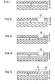
- Figure 1 is a cross-sectional view of an integrated circuit structure which may be fabricated using known process technology.
- the structure of Figure 1 is a fabricated by depositing N conductivity type polycrystalline silicon 12 on an underlying substrate 10.
- Polycrystalline layer 12 may be deposited as doped polycrystalline silicon to a thickness of 6000 Angstroms using chemical vapor deposition or may be deposited as relatively pure polycrystalline silicon which is subsequently doped by ion implantation, diffusion or other well known techniques.
- phosphorous is used to dope layer 12 to a concentration of 10 20 atoms per cubic centimeter.
- metal silicide 15 is deposited using chemical vapor deposition.
- metal silicide layer 15 is approximately 1000 Angstroms thick.
- Any electrically conductive silicide may be used, however, refractory metal silicides are preferred because of their ability to withstand subsequent high temperature processing operations to which the integrated circuit may be subjected.
- silicon dioxide layer 18 is formed on the upper surface of metal silicide 15 .
- silicon dioxide layer 18 is created by heating the underlying structure to a temperature of 1000°C in steam for 60 minutes to create a layer approximately 3000 Angstroms thick.
- the thickness of layer 18 need only be sufficient to assure that subsequently deposited layers of material on layer 18 will be electrically isolated from silicide layer 15.
- any material upon which polycrystalline silicon 12 may be deposited could be employed as the substrate. If an insulating material such as silicon dioxide is employed, the diode, or other circuit elements fabricated above silicon dioxide layer 10, will be electrical isolated from any structure beneath silicon dioxide layer 10. In some embodiments of the invention, however, this electrical isolation may not be desirable, and hence other materials may be employed as a substrate. In other embodiments of the invention, silicon dioxide layer 10 itself will be an insulating layer formed atop an integrated circuit containing other desired electronic components.
- an opening 20 is next made in a desired location through at least silicon dioxide 18 and metal silicide 15.
- This may be accomplished using well known photolithographic processes in conjunction with any desired chemical or plasma etching process.
- a plasma containing carbon tetrafluoride (CF 4 ) is used to etch through layer 18, while carbon tetrachloride (CC1 4 ) is used to etch through layer 15.
- CF 4 carbon tetrafluoride
- CC1 4 carbon tetrachloride
- the etching process is allowed to continue for a slightly longer time than is necessary to remove all of the silicide 15. This results in a slight etching of underlying pclycrystalline silicon 12 as shown, and assures that materials subsequently deposited in opening 20 will contact polycrystalline silicon 12.
- insulating material is then formed in opening 20 across the surface of polycrystalline silicon 12 and over the exposed edges of metal silicide 15. In the preferred embodiment this is accomplished by heating the structure to a temperature of 1000°C for a period of 10 minutes to create approximately 1000 Angstroms of silicon dioxide 18 in the bottom of the opening 20. It is essential to the subsequent fabrication steps described in conjunction with Figures 4 through 7 that insulating material 18 be formed over the sides of opening 20 to cover the exposed edges of silicide 15.
- an anisotropic etching process for example, plasma etching using carbon tetrafluoride, is employed to remove the silicon dioxide layer 18 from the bottom of opening 20.
- etching process for example, plasma etching using carbon tetrafluoride, is employed to remove the silicon dioxide layer 18 from the bottom of opening 20.
- the silicon dioxide 18 on the edges of layer 15 is not removed.
- a layer of polycrystalline silicon 22 is next deposited across the upper surface of the integrated circuit structure and suitably defined using well-known photolithographic and etching processes as shown in Figure 5.
- the polycrystalline silicon layer 22 is deposited using chemical vapor deposition to a thickness of 6000 Angstroms.
- the layer may be deposited as polycrystalline silicon doped P conductivity type, or may be deposited as relatively pure polycrystalline silicon and subsequently doped P conductivity type by ion implantation, diffusion, or other processes.
- boron is used to dope polycrystalline silicon 22 to an impurity concentration of 10 19 atoms per cubic centimeter.
- a PN junction 14 is created by the interface between P type polycrystalline silicon 22 and N type polycrystalline silicon 12.
- a layer of silicon dioxide or other insulating material 25 is formed across the upper surface of the integrated circuit structure.
- 3000 Angstroms of silicon dioxide 25 are formed by heating the integrated circuit structure in steam to a temperature of 1000°C for 60 minutes.
- the layer of silicon dioxide is then selectively removed using known photolithographic and etching techniques.
- An opening 27 is created to P type region 22 and an opening 28 is created to metal silicide 15.
- Ohmic connections (not shown) may be then be provided through openings 27 and 28 to P type region 22 and metal silicide 15. Fabrication of such ohmic connections is well known, and may utilize any conductive material, for example, aluminum.
- the contact through opening 28 provides an ohmic connection to the N conductivity type portion of PN junction 14, because silicide 15 provides a low resistance connection to polycrystalline silicon 12.
- Figure 7 is a top view of the structure shown in Figure 6.
- Figure 7 illustrates how the diode 14 of this invention may be fabricated at the intersection of two polycrystalline silicon lines 12 and 22.
- Figure 7 illustrates how only a single mask to define opening 20 (also shown in Figure 2) is necessary to fabricate the diode, with an additional mask being used to define the contact openings 27 and 28. Opening 27 is not shown in Figure 7.
- each of openings 27 and 28 may be made wider than the width of line 12 as shown in Figure 7.
- the enlarged sizes of the openings 27 and 28 simply cause any deposited material to contact either the desired regions or to harmlessly contact underlying silicon dioxide.
- the use of a single mask and self- alignment techniques permit-fabrication of an exceptionally compact diode.
Landscapes
- Electrodes Of Semiconductors (AREA)
- Bipolar Transistors (AREA)
Applications Claiming Priority (2)
| Application Number | Priority Date | Filing Date | Title |
|---|---|---|---|
| US31567781A | 1981-10-27 | 1981-10-27 | |
| US315677 | 1981-10-27 |
Publications (2)
| Publication Number | Publication Date |
|---|---|
| EP0078221A2 true EP0078221A2 (de) | 1983-05-04 |
| EP0078221A3 EP0078221A3 (de) | 1986-06-11 |
Family
ID=23225556
Family Applications (1)
| Application Number | Title | Priority Date | Filing Date |
|---|---|---|---|
| EP82401971A Ceased EP0078221A3 (de) | 1981-10-27 | 1982-10-26 | Polykristalline Siliziumdiode mit einem Kontakt aus Metallsilicid |
Country Status (3)
| Country | Link |
|---|---|
| EP (1) | EP0078221A3 (de) |
| JP (1) | JPS5882577A (de) |
| CA (1) | CA1198832A (de) |
Cited By (1)
| Publication number | Priority date | Publication date | Assignee | Title |
|---|---|---|---|---|
| EP0212207A1 (de) * | 1985-07-19 | 1987-03-04 | Siemens Aktiengesellschaft | Bipolartransistorstruktur für integrierte Schaltungen mit hohen Schaltgeschwindigkeiten und Verfahren zu ihrer Herstellung |
Families Citing this family (1)
| Publication number | Priority date | Publication date | Assignee | Title |
|---|---|---|---|---|
| JPH0642555B2 (ja) * | 1989-06-20 | 1994-06-01 | 株式会社東芝 | 半導体装置 |
Family Cites Families (5)
| Publication number | Priority date | Publication date | Assignee | Title |
|---|---|---|---|---|
| NL190710C (nl) * | 1978-02-10 | 1994-07-01 | Nec Corp | Geintegreerde halfgeleiderketen. |
| US4256514A (en) * | 1978-11-03 | 1981-03-17 | International Business Machines Corporation | Method for forming a narrow dimensioned region on a body |
| JPS55134962A (en) * | 1979-04-09 | 1980-10-21 | Toshiba Corp | Semiconductor device |
| CA1142261A (en) * | 1979-06-29 | 1983-03-01 | Siegfried K. Wiedmann | Interconnection of opposite conductivity type semiconductor regions |
| US4488350A (en) * | 1981-10-27 | 1984-12-18 | Fairchild Camera & Instrument Corp. | Method of making an integrated circuit bipolar memory cell |
-
1982
- 1982-10-26 EP EP82401971A patent/EP0078221A3/de not_active Ceased
- 1982-10-26 CA CA000414201A patent/CA1198832A/en not_active Expired
- 1982-10-27 JP JP57187640A patent/JPS5882577A/ja active Pending
Cited By (1)
| Publication number | Priority date | Publication date | Assignee | Title |
|---|---|---|---|---|
| EP0212207A1 (de) * | 1985-07-19 | 1987-03-04 | Siemens Aktiengesellschaft | Bipolartransistorstruktur für integrierte Schaltungen mit hohen Schaltgeschwindigkeiten und Verfahren zu ihrer Herstellung |
Also Published As
| Publication number | Publication date |
|---|---|
| EP0078221A3 (de) | 1986-06-11 |
| JPS5882577A (ja) | 1983-05-18 |
| CA1198832A (en) | 1985-12-31 |
Similar Documents
| Publication | Publication Date | Title |
|---|---|---|
| US3825442A (en) | Method of a semiconductor device wherein film cracking is prevented by formation of a glass layer | |
| CA2034075C (en) | Self-aligning contact and interconnect structure | |
| US4512073A (en) | Method of forming self-aligned contact openings | |
| US4384301A (en) | High performance submicron metal-oxide-semiconductor field effect transistor device structure | |
| US4234357A (en) | Process for manufacturing emitters by diffusion from polysilicon | |
| US4446613A (en) | Integrated circuit resistor and method of fabrication | |
| EP0126424A2 (de) | Verfahren zur Herstellung von Polycide-Strukturen | |
| US5473184A (en) | Semiconductor device and method for fabricating same | |
| US4714686A (en) | Method of forming contact plugs for planarized integrated circuits | |
| JPS61503064A (ja) | リンにてゲッタリングされる半導体集積回路 | |
| EP0054163A2 (de) | Verfahren zur Herstellung eines elektrischen Kontakts zu einem Siliziumsubstrat durch eine auf einer Substratoberfläche angebrachte, verhältnismässig dünne Schicht aus Siliziumdioxyd und Verfahren zur Herstellung eines Feldeffekttransistors | |
| EP0076105A2 (de) | Verfahren zur Herstellung eines bipolaren Transistors | |
| US4425379A (en) | Polycrystalline silicon Schottky diode array | |
| EP0062417B1 (de) | Einen Transistor und einen Kondensator enthaltendes Halbleiterbauelement und Verfahren zu seiner Herstellung | |
| US4700465A (en) | Method of selectively making contact structures both with barrier metal and without barrier metal in a single process flow | |
| EP0078220B1 (de) | Polykristalline Silizium-Verbindungen für Bipolartransistoren in Flip-Flop-Schaltung | |
| EP0051534A2 (de) | Selbstjustierendes Verfahren zur Herstellung integrierter Stromkreisstrukturen unter Verwendung unterschiedlicher Oxydationsraten | |
| US4090915A (en) | Forming patterned polycrystalline silicon | |
| US4081896A (en) | Method of making a substrate contact for an integrated circuit | |
| EP0144762A1 (de) | Verfahren zum Herstellen eng benachbarter Öffnungen und zum Kontaktieren der Oberflächen von Halbleiterbauelementen | |
| EP0077737A2 (de) | Feldeffekttransistor mit kleiner Kapazität | |
| US4883772A (en) | Process for making a self-aligned silicide shunt | |
| US4628339A (en) | Polycrystalline silicon Schottky diode array | |
| US5175127A (en) | Self-aligned interlayer contact process using a plasma etch of photoresist | |
| EP0621631A1 (de) | Verfahren zur Herstellung von Widerständen für integrierte Schaltkreise unter Verwendung von Gräben |
Legal Events
| Date | Code | Title | Description |
|---|---|---|---|
| PUAI | Public reference made under article 153(3) epc to a published international application that has entered the european phase |
Free format text: ORIGINAL CODE: 0009012 |
|
| AK | Designated contracting states |
Designated state(s): DE FR GB IT NL |
|
| PUAL | Search report despatched |
Free format text: ORIGINAL CODE: 0009013 |
|
| AK | Designated contracting states |
Kind code of ref document: A3 Designated state(s): DE FR GB IT NL |
|
| 17P | Request for examination filed |
Effective date: 19861210 |
|
| 17Q | First examination report despatched |
Effective date: 19880706 |
|
| RAP1 | Party data changed (applicant data changed or rights of an application transferred) |
Owner name: FAIRCHILD SEMICONDUCTOR CORPORATION |
|
| STAA | Information on the status of an ep patent application or granted ep patent |
Free format text: STATUS: THE APPLICATION HAS BEEN REFUSED |
|
| 18R | Application refused |
Effective date: 19881230 |
|
| RIN1 | Information on inventor provided before grant (corrected) |
Inventor name: VORA, MADHUKAR B. |