EP0077136A2 - Protecteur de ligne et dispositif répartiteur afférent - Google Patents
Protecteur de ligne et dispositif répartiteur afférent Download PDFInfo
- Publication number
- EP0077136A2 EP0077136A2 EP82305007A EP82305007A EP0077136A2 EP 0077136 A2 EP0077136 A2 EP 0077136A2 EP 82305007 A EP82305007 A EP 82305007A EP 82305007 A EP82305007 A EP 82305007A EP 0077136 A2 EP0077136 A2 EP 0077136A2
- Authority
- EP
- European Patent Office
- Prior art keywords
- connector
- insulator
- line
- housing
- contacts
- Prior art date
- Legal status (The legal status is an assumption and is not a legal conclusion. Google has not performed a legal analysis and makes no representation as to the accuracy of the status listed.)
- Withdrawn
Links
Images


Classifications
-
- H—ELECTRICITY
- H04—ELECTRIC COMMUNICATION TECHNIQUE
- H04Q—SELECTING
- H04Q1/00—Details of selecting apparatus or arrangements
- H04Q1/18—Electrical details
- H04Q1/28—Current-supply circuits or arrangements for selection equipment at exchanges
-
- H—ELECTRICITY
- H04—ELECTRIC COMMUNICATION TECHNIQUE
- H04Q—SELECTING
- H04Q1/00—Details of selecting apparatus or arrangements
- H04Q1/02—Constructional details
- H04Q1/14—Distribution frames
- H04Q1/146—Distribution frames with line protection means
Definitions
- This invention relates generally to telephone circuit distribution systems, and more particularly to systems having overload protector modules that provide line protection for the inside plant equipment, such as central office switching equipment and the like.
- modules are known. The most common is the type with line terminal pins that plug into holes in the connector. However, with pin terminal type modules there is a practical limit to the size to which the module can be reduced. Furthermore, the connector itself can only be reduced by so much because the connector must retain a pattern of holes compatible with the module pins.
- An object of this invention is to provide a novel line protector for a communications circuit plus a new "panel" or connector which interfaces the line protector to form a termination structure that is relatively small as compared to current commercially available arrangements,
- a further object of this invention is to provide an arrangement of the type stated in which the module utilizes a printed circuit board for substantially all of its internal wiring and also utilizes that same printed circuit board for the ground and line terminals of the module.
- An additional object of this invention is to provide a module of the type stated which can be plugged into a standard printed circuit board edge connector but which connector is modified to provide a ground buss which occupies only a minimum of space.
- Another object of this invention is to provide a module and edge connector arrangement that can be utilized, for example, in 25 pair groups to be compatible with 25 pair cable groups. If desired each 25 pair or other designated group and associated wiring may be a package complete in itself. Consequently, any number of 25 pair groups may be added or subtracted to an array which may typically be a 900 pair assembly on a main distribution frame.
- a still further object of this invention is to provide an-arrester module of the type stated which has a unique method of providing a so-called "detent” position.
- the line from the inside plant equipment to the protector is an open circuit.
- the circuit is opened by a sliding insulator which is shiftable from a first position in which the inside line circuit is closed to a second position in which the insulator acts to open the inside line circuit.
- the invention provides an arrangement by which the accidental bumping of the module, which might cause it to change its preset position, is effectively prevented.
- means are provided for visually detecting the position of the insulator through a window or slot in the handle of the module.
- the invention comprises a line protector with a housing having opposite ends,'a printed circuit board in said housing and having a part thereof projecting from one of said housing ends, first and second line terminals printed on said board and being electrically insulated from each other, a ground terminal printed on said board and being electrically insulated from each of said line terminals, said printed terminals extending from within the housing to said projected part of the board so as to lie outwardly of said housing and adjacent to one another, a first contact in said housing adjacent to said one end and being electrically connected to said first line terminal, a second contact in said housing adjacent to the other end of said housing being electrically connected to said second terminal, and a third contact in said housing intermediate the first and second contacts and being electrically connected to said ground terminal; and surge voltage arrester means between said first and second contacts and having a first electrode electrically connected to said first contact, a second electrode electrically connected to said second contact, and a ground electrode structure electrically connected to said third contact; each of said contacts being secured to the printed circuit
- the insulator referred to previously is a flat sheet movable relative to said board to overlie the portions of said first and second terminals that are on said projected part while leaving exposed the ground terminal portion on said projected part.
- a termination structure comprising a housing, a surge voltage arrester in said housing and having opposed contacts, a line terminal electrically connected to one of said contacts and adapted to be connected to a line to be protected, a ground terminal electrically connected to the other of said contacts such that a surge on said line will be shunted through said arrester to said ground terminal, said terminals having parts projecting outwardly of said housing, a connector having a recess, contacts in said recess for plug-in engagement with said outwardly projected parts of said terminals, and an insulator adjacent to the outwardly projected part of a line terminal and shiftable to and from a first position that is free from obstructing the engagement of said outwardly projected line terminal part with its associated contact when said terminals are plugged into said connector to a second position in which said insulator is between said associated contact and line terminal part to interrupt the circuit from said associated contact to said surge voltage arrester.
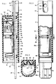
- a protector module 2 comprising a generally rectilinear housing 4 of plastic or like dielectric material and having opposite ends. At one end of the housing 4 is a bifurcated handle 6 that provides a window or slot 8 for purposes presently more fully appearing. At its other end the housing 4 receives a base 10 of like plastic and which may be snapped into place as best seen in FIG. 7.
- opposed walls of the housing 4 are provided with notches 12, 12 that receive nibs 14 on the base 10. The opposed housing walls are sufficiently yieldable within elastic limits to allow the nibs 14 to pass thereover and snap fit into the notches 12.
- a dielectric printed circuit board 16 Positioned within the housing 2 is a dielectric printed circuit board 16 having an upper bifurcated end portion 18 that lies within a pocket 20 that is formed by the plastic at the handle 6. The end of the pocket 20 is closed off by a section of plastic 22, and marginal portions of the plastic of the handle define the window or slot 8.
- the printed circuit board also fits in a pair of opposed channels 24, 24 on opposite sides of the housing, and the lower portion 26 of the printed circuit board project outwardly from the housing, as best seen in FIGS. 1 and 2. It will be noted that the housing, as illustrated in FIGS. 1 and 2, is inverted from the positions of the housing shown in FIGS. 8-10. In any event, the printed circuit board 16 fits snugly within the housing, and the back side of the printed circuit board faces a clearance channel 28. The forward side of the printed circuit board is presented to the main cavity 30 of the module for purposes presently more fully appearing.
- the printed wiring on the printed circuit board 16 is best shown in FIGS. 4 and 5. Because of the scale of the drawing, the printed circuit wiring is not shown in FIGS. 1-3, 7-10 and 12.
- the printed circuit wiring includes a first line terminal 32, a second line terminal 34 and ground terminal 36.
- the patterns of the respective terminals 32, 34, 36 are, as shown in FIG. 4, insulated from each other.
- the reverse side of the printed circuit board is shown in FIG. 5.
- Imprinted thereon are line terminal wirings 32a, 34a and ground terminal wiring 36a which correspond to and are in registration respectively with the printed wirings 32, 34, 36.
- Each terminal 32, 32a or 34, 34a or 36, 36a includes a mounting hole region 38, 40, 42 which regions are preferably equally spaced along the length of the printed circuit board.
- each contact plate 44, 46, 48 Projecting through the mounting holes at the regions 38, 40, 42 are parallel metal contact plates 44, 46, 48 which are parallel to each other and perpendicular to the plane of the printed circuit board.
- Each contact plate 44, 46, 48 includes a nib 50 that projects through the printed circuit board and is secured by solder 52, whereby the nibs 50 and the solder 52 occupy portions of the clearance channel 28.
- electrical continuity is established between the printed wiring portions of the respective terminals on opposite sides of the printed circuit board.
- the outwardly projected part 26 of the printed circuit board includes outwardly projected terminals portions 32b, 34b, 36b on both sides of the printed circuit board and which are parallel to each other for insertion into the circuit board edge connector shown in FIGS. 8-12, as will be presently more fully described.
- a surge voltage arrester 53 comprising a pair of carbon electrodes 54, 56 that define an arc gap 58 therebetween.
- the electrode 56 is surrounded by and is mounted in a tubular ceramic insulator 60 upon which is seated the electrode 54. Electrode 56 is recessed within the ceramic to the extent necessary to establish the arc gap 58.
- a solder ring 62 is located between the electrode 54 and the end of a metallic cup 66 which houses the electrodes 54, 56, the ceramic 60 and the solder 62.
- a U-shaped conductive spring is disposed between the cup 66 and the contact plate 44 to provide a conductive connection between the plate 44 and the electrode 54. The spring 68 also presses electrode 56 into contact with the plate 46.
- an insulator barrier is inserted between the arrester unit cups and the printed circuit board.
- a rectangular sheet 70 of insulating material is disposed between the plates 44, 46, 48 and the surface of the printed circuit board.
- the sheet 70 is notched as in 72, 72, 72 for receiving the respective plates 44, 46, - 48 and by which the insulating sheet 70 is secured in place.
- the insulator 74 is provided with three elongated slots 76, 76, 76 through which the plates 44, 46, 48 project; however, the elongated slot 76 permits longitudinal movement of the insulator 74.
- the insulator 74 has a hole 78 which is exposed to the window 8 and through which a tool may be inserted for manipulating the insulator 74.
- the insulator 74 is cut away in the region of the ground terminal part 36b so that when the insulator 74 is shifted so that its end nearest the plate. 48 covers the terminal portions 32b, 34b, the ground terminal portion 36b will still remain exposed.
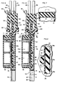
- FIGS. 9-12 there is shown a module mounted on an edge connector 80. Only one module is shown, it being apparent that other modules of like construction may be mounted next to the module shown so as to fill up the edge connector 80.
- the printed circuit board edge connector 80 has a long narrow plastic dielectric body with two rows of terminals 82, 84. Such an edge connector is economical on space.
- the row 82 may be considered as having a tip out terminal 86, a ring out terminal 88 and a ground terminal 90.
- the edge connector is secured to a main distribution frame or like support 96 through bolt and nut assemblies 98 and through which the ground buss 94 is electrically connected to the frame 96 for grounding purposes.
- Other like edge connectors may be secured to the main frame in a similar manner.
- the edge connector has a recess 100 in. which the terminals 86, 88, 92 etc. are bowed to form resilient arcuate terminations 93 that spread apart to receive the edge portion 26 of the circuit board 16.
- the terminal 32 With the insulator 74 retracted, namely as shown in FIG. 9, the terminal 32 will be in electrical contact with the tip in and tip out terminals 96 to provide protection through the surge arrester 53a.
- the ring in and ring out terminals will be in conductive connection with the printed circuit board terminal 34 to provide protection for the ring side of the line through the surge voltage arrester 53. Ground will be maintained through the ground terminals 90 which contact the printed circuit board ground terminal 36.
- a suitable tool may be inserted into the hole 78 whereupon the insulator 74 may be pushed toward the edge connector 80 until the end of the insulator 74 separates the tip out terminal 86 from the adjacent printed circuit board terminal 32 (FIG. ll).
- the ring out terminal is separated from the printed circuit board terminal 36 so that the insulator 74 opens both the tip and ring circuits to the central office or inside plant equipment.
- the ground circuits through the arresters 53, 53a from tip in and ring in remain unaffected because the insulator 74 is cut away as previously described and so does not interrupt the ground circuits.
- Resetting the protector module for normal use is relatively simple. This can be done by inserting a tool in the hole 78 to retract the insulator 74 from the edge connector contact parts 93. Additionally, the module may be grasped by its handle 6 and completely extracted from its position in the edge connector and then pushed back fully into the edge connector. This causes the sliding insulator 74 to shift and automatically reset itself to its non-detent position (FIG. 9).
- a plastic bezel 102 fits over the opening into the edge connector cavity 100.
- This' bezel 102 is secured to the frame 96 by spring clips 104.
- the bezel has a series of elongated slots 106 (FIG. 12) each for receiving the printed circuit board of one module.
- the slot includes a polarizing recess 108 that receives a polarizing nib 110 on the base 10 of the housing. This nib 110 insures that the module is plugged in correctly.
Applications Claiming Priority (2)
| Application Number | Priority Date | Filing Date | Title |
|---|---|---|---|
| US06/310,473 US4390921A (en) | 1981-10-13 | 1981-10-13 | Line protector and related termination arrangement |
| US310473 | 1981-10-13 |
Publications (2)
| Publication Number | Publication Date |
|---|---|
| EP0077136A2 true EP0077136A2 (fr) | 1983-04-20 |
| EP0077136A3 EP0077136A3 (fr) | 1984-02-29 |
Family
ID=23202673
Family Applications (1)
| Application Number | Title | Priority Date | Filing Date |
|---|---|---|---|
| EP82305007A Withdrawn EP0077136A3 (fr) | 1981-10-13 | 1982-09-23 | Protecteur de ligne et dispositif répartiteur afférent |
Country Status (9)
| Country | Link |
|---|---|
| US (1) | US4390921A (fr) |
| EP (1) | EP0077136A3 (fr) |
| JP (1) | JPS5873297A (fr) |
| KR (1) | KR860000987B1 (fr) |
| AR (1) | AR229370A1 (fr) |
| BR (1) | BR8205949A (fr) |
| CA (1) | CA1180373A (fr) |
| MX (1) | MX152048A (fr) |
| ZA (1) | ZA826931B (fr) |
Cited By (1)
| Publication number | Priority date | Publication date | Assignee | Title |
|---|---|---|---|---|
| RU2485177C1 (ru) * | 2012-03-07 | 2013-06-20 | Федеральное Государственное Бюджетное Учреждение науки Институт химической биологии и фундаментальной медицины Сибирского отделения РАН (ИХБФМ СО РАН) | СПОСОБ ВЫЯВЛЕНИЯ УСТОЙЧИВЫХ К РИФАМПИЦИНУ ИЗОЛЯТОВ Mycobacterium tuberculosis |
Families Citing this family (5)
| Publication number | Priority date | Publication date | Assignee | Title |
|---|---|---|---|---|
| US4924345A (en) * | 1988-05-04 | 1990-05-08 | The Siemon Company | Combined transient voltage and sneak current protector |
| US5177782A (en) * | 1990-08-30 | 1993-01-05 | Minnesota Mining And Manufacturing Company | Modular protected entrance terminal |
| DE102009010929A1 (de) * | 2009-02-27 | 2010-09-09 | Adc Gmbh | Überspannungsschutzmagazin oder -stecker und Verfahren zur Herstellung eines Überspannungsschutzmagazins oder -steckers |
| US8995106B2 (en) * | 2011-02-08 | 2015-03-31 | Raycap, S.A. | Overvoltage protection system for wireless communication systems |
| KR20190109049A (ko) | 2018-03-16 | 2019-09-25 | 조명숙 | 전주작업용 안전장치 |
Citations (2)
| Publication number | Priority date | Publication date | Assignee | Title |
|---|---|---|---|---|
| FR2341974A1 (fr) * | 1976-02-18 | 1977-09-16 | Causse Raoul | Dispositif de protection de lignes basse tension, notamment pour reseau telephonique |
| FR2399143A1 (fr) * | 1977-07-28 | 1979-02-23 | Constr Telephoniques | Fiche isolante verrouillable pour reglette de coupure |
Family Cites Families (12)
| Publication number | Priority date | Publication date | Assignee | Title |
|---|---|---|---|---|
| US3255330A (en) * | 1962-08-30 | 1966-06-07 | Cook Electric Co | Line protector |
| JPS4810243B1 (fr) * | 1967-11-01 | 1973-04-02 | ||
| US3567998A (en) * | 1968-05-13 | 1971-03-02 | Rca Corp | Corner edge connector for printed circuit boards |
| US3518611A (en) * | 1968-07-10 | 1970-06-30 | Bell Telephone Labor Inc | Connector for telephone main distributing frame |
| US3535463A (en) * | 1968-12-13 | 1970-10-20 | Felice Trucco | Section strip for use particularly in telephone equipment |
| US3587021A (en) * | 1969-07-22 | 1971-06-22 | Reliable Electric Co | Line protector for a communications circuit |
| JPS4882360A (fr) * | 1972-02-07 | 1973-11-02 | ||
| US3760328A (en) * | 1972-04-19 | 1973-09-18 | Gte Automatic Electric Lab Inc | Telephone type electrical connectors |
| US3947732A (en) * | 1973-02-27 | 1976-03-30 | Cook Electric Company | Connector block for telephone central office main distributing frame |
| US4017770A (en) * | 1974-11-22 | 1977-04-12 | Applicazione Elettrotelefoniche Spa | Connecting device for telecommunication circuits |
| US4057692A (en) * | 1976-10-27 | 1977-11-08 | Northern Telecom Limited | Protector apparatus for telecommunications lines |
| US4325100A (en) * | 1980-06-12 | 1982-04-13 | Reliable Electric Company | Line protector for a communications circuit |
-
1981
- 1981-10-13 US US06/310,473 patent/US4390921A/en not_active Expired - Fee Related
-
1982
- 1982-09-21 ZA ZA826931A patent/ZA826931B/xx unknown
- 1982-09-23 EP EP82305007A patent/EP0077136A3/fr not_active Withdrawn
- 1982-09-28 CA CA000412320A patent/CA1180373A/fr not_active Expired
- 1982-10-07 AR AR290909A patent/AR229370A1/es active
- 1982-10-08 JP JP57178230A patent/JPS5873297A/ja active Pending
- 1982-10-11 BR BR8205949A patent/BR8205949A/pt unknown
- 1982-10-11 MX MX194747A patent/MX152048A/es unknown
- 1982-10-12 KR KR8204578A patent/KR860000987B1/ko active IP Right Grant
Patent Citations (2)
| Publication number | Priority date | Publication date | Assignee | Title |
|---|---|---|---|---|
| FR2341974A1 (fr) * | 1976-02-18 | 1977-09-16 | Causse Raoul | Dispositif de protection de lignes basse tension, notamment pour reseau telephonique |
| FR2399143A1 (fr) * | 1977-07-28 | 1979-02-23 | Constr Telephoniques | Fiche isolante verrouillable pour reglette de coupure |
Cited By (1)
| Publication number | Priority date | Publication date | Assignee | Title |
|---|---|---|---|---|
| RU2485177C1 (ru) * | 2012-03-07 | 2013-06-20 | Федеральное Государственное Бюджетное Учреждение науки Институт химической биологии и фундаментальной медицины Сибирского отделения РАН (ИХБФМ СО РАН) | СПОСОБ ВЫЯВЛЕНИЯ УСТОЙЧИВЫХ К РИФАМПИЦИНУ ИЗОЛЯТОВ Mycobacterium tuberculosis |
Also Published As
| Publication number | Publication date |
|---|---|
| US4390921A (en) | 1983-06-28 |
| MX152048A (es) | 1985-05-24 |
| KR840002385A (ko) | 1984-06-25 |
| EP0077136A3 (fr) | 1984-02-29 |
| KR860000987B1 (ko) | 1986-07-24 |
| ZA826931B (en) | 1983-09-28 |
| BR8205949A (pt) | 1983-09-13 |
| JPS5873297A (ja) | 1983-05-02 |
| AR229370A1 (es) | 1983-07-29 |
| CA1180373A (fr) | 1985-01-02 |
Similar Documents
| Publication | Publication Date | Title |
|---|---|---|
| CA1067953A (fr) | Protecteur de ligne pour circuit de communication | |
| KR970004154B1 (ko) | 차폐 모듈 잭 | |
| US4741711B1 (fr) | ||
| US4602842A (en) | Electrical connector receptacle | |
| US4331839A (en) | Telephone distribution frame connector assembly | |
| US4422121A (en) | Line protector for a communications circuit | |
| US20030228781A1 (en) | High frequency coaxial jack | |
| EP0037222B1 (fr) | Protecteur de ligne pour un circuit de télécommunication | |
| KR960008200B1 (ko) | 터미날 테스트 플러그 | |
| US4993971A (en) | EMI resistant electrical connector | |
| US4390921A (en) | Line protector and related termination arrangement | |
| US5154639A (en) | Protective plug for a distributor strip utilized in telecommunications systems | |
| US6093041A (en) | Connector block with internal power bus | |
| US4882748A (en) | Homologated protector modules for telephone connector blocks | |
| US4400645A (en) | CRT Socket assembly | |
| US4288660A (en) | Test cord for telephone circuits | |
| US6540534B2 (en) | Telephone wiring interconnect apparatus and method | |
| US5883953A (en) | Telephone and data communications line protection module and grounding spring clip | |
| IE903008A1 (en) | Protective device for a distributor in a telecommunication¹system | |
| US5487675A (en) | Integrated protector and modular jack | |
| JPS6311872Y2 (fr) | ||
| AU741657B2 (en) | Electrical connector | |
| US8005205B2 (en) | Protective plug for distribution frame devices in telecommunications and data technology | |
| GB1155540A (en) | Main Distributing Frame and Switching Arrangements |
Legal Events
| Date | Code | Title | Description |
|---|---|---|---|
| PUAI | Public reference made under article 153(3) epc to a published international application that has entered the european phase |
Free format text: ORIGINAL CODE: 0009012 |
|
| AK | Designated contracting states |
Designated state(s): DE FR GB |
|
| PUAL | Search report despatched |
Free format text: ORIGINAL CODE: 0009013 |
|
| AK | Designated contracting states |
Designated state(s): DE FR GB |
|
| STAA | Information on the status of an ep patent application or granted ep patent |
Free format text: STATUS: THE APPLICATION IS DEEMED TO BE WITHDRAWN |
|
| 18D | Application deemed to be withdrawn |
Effective date: 19841030 |
|
| RIN1 | Information on inventor provided before grant (corrected) |
Inventor name: BAUMBACH, BERTRAM WILLIAM |