EP0076645B1 - Method of and apparatus for transmitting a call charging signal - Google Patents
Method of and apparatus for transmitting a call charging signal Download PDFInfo
- Publication number
- EP0076645B1 EP0076645B1 EP82305179A EP82305179A EP0076645B1 EP 0076645 B1 EP0076645 B1 EP 0076645B1 EP 82305179 A EP82305179 A EP 82305179A EP 82305179 A EP82305179 A EP 82305179A EP 0076645 B1 EP0076645 B1 EP 0076645B1
- Authority
- EP
- European Patent Office
- Prior art keywords
- signal
- pulse code
- circuit
- code signal
- charging
- Prior art date
- Legal status (The legal status is an assumption and is not a legal conclusion. Google has not performed a legal analysis and makes no representation as to the accuracy of the status listed.)
- Expired
Links
Images


Classifications
-
- H—ELECTRICITY
- H04—ELECTRIC COMMUNICATION TECHNIQUE
- H04W—WIRELESS COMMUNICATION NETWORKS
- H04W84/00—Network topologies
- H04W84/02—Hierarchically pre-organised networks, e.g. paging networks, cellular networks, WLAN [Wireless Local Area Network] or WLL [Wireless Local Loop]
- H04W84/10—Small scale networks; Flat hierarchical networks
- H04W84/14—WLL [Wireless Local Loop]; RLL [Radio Local Loop]
-
- G—PHYSICS
- G08—SIGNALLING
- G08C—TRANSMISSION SYSTEMS FOR MEASURED VALUES, CONTROL OR SIMILAR SIGNALS
- G08C25/00—Arrangements for preventing or correcting errors; Monitoring arrangements
-
- H—ELECTRICITY
- H04—ELECTRIC COMMUNICATION TECHNIQUE
- H04M—TELEPHONIC COMMUNICATION
- H04M15/00—Arrangements for metering, time-control or time indication ; Metering, charging or billing arrangements for voice wireline or wireless communications, e.g. VoIP
- H04M15/28—Arrangements for metering, time-control or time indication ; Metering, charging or billing arrangements for voice wireline or wireless communications, e.g. VoIP with meter at substation or with calculation of charges at terminal
-
- H—ELECTRICITY
- H04—ELECTRIC COMMUNICATION TECHNIQUE
- H04M—TELEPHONIC COMMUNICATION
- H04M17/00—Prepayment of wireline communication systems, wireless communication systems or telephone systems
- H04M17/02—Coin-freed or check-freed systems, e.g. mobile- or card-operated phones, public telephones or booths
- H04M17/023—Circuit arrangements
-
- H—ELECTRICITY
- H04—ELECTRIC COMMUNICATION TECHNIQUE
- H04W—WIRELESS COMMUNICATION NETWORKS
- H04W4/00—Services specially adapted for wireless communication networks; Facilities therefor
- H04W4/24—Accounting or billing
-
- H—ELECTRICITY
- H04—ELECTRIC COMMUNICATION TECHNIQUE
- H04M—TELEPHONIC COMMUNICATION
- H04M2215/00—Metering arrangements; Time controlling arrangements; Time indicating arrangements
- H04M2215/32—Involving wireless systems
Definitions
- This invention relates to a method of and apparatus for transmitting a call charging signal.
- a call charging signal for indicating the charge for or cost of a call to a user, is generated by an exchange and transmitted to the telephone (for example, a public telephone) via the wires.
- a carrier signal of frequency such as 50 Hz, 12 kHz or 16 kHz, or a polarity inverting signal, is used and users are given call charges by transmitting such specified frequency signals for example, at particular time intervals.
- the call charging signals In a telephone service system in which exchanges and telephones are connected by way of radio links, the call charging signals must be sent to the telephone side via a radio link.
- Such a charging signal is transmitted during conversation together with a voice signal and therefore it is essential to prevent such a charging signal interfering with a voice signal.
- a method of transmitting a call charging signal in a telephone system having an exchange and a user telephone characterised by the steps of:
- the present invention is concerned with a signal transmission system in which an exchange and a public or user's telephone system are connected via a radio link and a call charging signal sent from the exchange is transmitted by radio equipment to the user's telephone system.
- An embodiment of this invention can provide for the transmission of a call charging signal as a signal of a frequency outside the voice transmitting frequency band (an out-of-band frequency) with the prevention of errors in a charge processing circuit, provided in a public telephone system, resulting from noise.
- An embodiment of this invention can provide that a call charging signal carrier (the encoded charging signal modulated by the out-of-band frequency) is reliably transmitted even when the voice signal onto which the charging signal carrier is superimposed is subjected to amplitude limitation in a stage preceding a modulator circuit provided in radio equipment for signal transmission, and can provide that the S/N ratio (signal to noise ratio) is not worsened when the call charging signal is not being transmitted.
- a call charging signal carrier the encoded charging signal modulated by the out-of-band frequency
- radio equipment on the side of an exchange detects a charging signal sent from the exchange and encodes it into a pulse code signal consisting of plurality of continuous pulses in order to transmit the charging signal sent from the exchange to the telephone side, by radio equipment, together with a voice signal.
- This pulse code signal is modulated by a frequency outside the frequency band used for transmitting a voice signal and then transmitted.
- radio equipment on the telephone side detects the frequency signal outside the voice frequency band and demodulates it into the pulse code signal and counts the continuous pulses of the pulse code signal. When the counted value reaches a specified value, the radio equipment on the telephone side generates a charging signal, thereby to regenerate the charging signal sent from exchange side, and then transmits it to the telephone system of a user.
- a circuit which more deeply limits the amplitude of a voice signal than is ordinarily the case is provided in the radio equipment on the exchange side.
- This amplitude limiter circuit is operated in synchronization with a charging signal carrier to be superimposed on the voice signal in desired time intervals, and thereafter the charging signal carrier is superimposed on the amplitude-limited voice signal.
- the resultant signal is subjected to ordinary amplitude limitation and modulated, followed by transmission to the radio equipment on the telephone side.
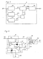
- FIG. 1 is a block diagram of principal parts of an embodiment of this invention for transmitting a call charging signal.
- a charging signal generated from an exchange 1 is detected by a charging signal detecting circuit 3 of radio equipment 2 and is encoded into a pulse code signal by a pulse encoder circuit 4.
- An out-of-band frequency signal for example a signal of 3825 Hz in a case in which the voice band is 200 Hz to 3.4 kHz, is generated in accordance with the pulse code signal by an out-of-band frequency generating circuit 5 and the out-of-band frequency signal is modulated together with a voice signal (on to a carrier) and transmitted via a radio link 6.
- Radio equipment 7 on the side of a public telephone set 12 detects and demodulates the 3825 Hz signal by means of an out-of-band frequency detecting circuit 8 and the detected and demodulated signal is applied to a pulse counter circuit 9.
- a charging signal regenerating circuit 10 regenerates a charging signal by having applied thereto a control signal provided when the counter value in the pulse counter circuit reaches a specified value. This charging signal is applied to a charging signal processing circuit 11 associated with telephone set 12.
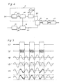
- Figure 2 shows waveforms for assistance in explaining operations of the arrangement of Figure 1.
- a detection signal as shown in Figure 2(a) is output from circuit 3.
- the pulse encoder circuit 4 outputs a pulse code signal shown in Figure 2(b).
- This pulse code signal for example consists of a continuous pulse stream having a duty ratio of 50% with a pulse period of 16 mS.
- the out-of-band frequency generating circuit 5 outputs a signal of an out-of-band frequency, such as 3825 Hz etc., through switching operations effected in response to the pulse code signal and an output as shown in Figure 2(c) is obtained.
- the radio equipment 7 on the telephone side detects and demodulates the out-of-band frequency signal of 3825 Hz by means of the out-of-band frequency detecting circuit 8 and performs waveform shaping and outputs a pulse code signal as shown in Figure 2(d).
- the pulse counter circuit 9 counts the continuous pulses of this pulse code signal and starts the charging signal regenerating circuit 10 for example in dependence upon the count of the pulses and the circuit 10 outputs a charging signal at a time t, as shown in Figure 2(e).
- the charging signal is transmitted and received as an out-of-band frequency signal, no interference with a voice signal results therefrom. Further, since the charging signal is transmitted as a modulated pulse code signal and the received charging signal is demodulated to provide a pulse code signal, and since this pulse code signal is continuously counted and confirmation of receipt of a charging signal given when a specified count value is reached, noise signals are not taken to be charging signals.
- a charging signal is generated in the radio equipment on the telephone side only after checking for a predetermined pulse count value, such as 3,4 or 5 pulses, and consequently a momentary pulse signal resulting from noise at an out-of-band frequency, such as FM noise, ignition noise etc., or a continuous signal, can be distinguished from charging signals since they will not provide the proper pulse count, and thereby erroneous charging can be prevented.
- a predetermined pulse count value such as 3,4 or 5 pulses
- FIG. 3 is a block diagram of pulse counter circuit 9 of radio equipment 7 shown in Figure 1.
- a pulse signal sent from the out-of-band frequency detecting circuit 8 is applied to a filter 91, an idle condition detecting circuit 92 and a continuous signal condition detecting circuit 93.
- a counter 95 counts pulses of the pulse signal sent from the filter 91 and is reset by a detection signal from either of detecting circuits 92, 93 via an OR circuit 94.
- a judgement output circuit 96 judges when the count value of counter 95 reaches the specified predetermined count value and outputs a start signal for charging signal regenerating circuit 10.
- Figure 4 shows a practical circuit configuration of the pulse counter circuit of Figure 3
- Figure 5 shows signal waveforms for assistance in explaining operations of the circuit of Figure 4.
- a resistor R1 and a capacitor C1 form the filter 91; an inverter G1, a diode D1, a resistor R2, and a capacitor C2 form the idle condition detecting circuit 92; a diode D2, a resistor R3 and a capacitor C3 form the continuous signal condition detecting circuit 93; an OR circuit G2 corresponds to the OR circuit 94; a counter CTR corresponds to the counter 95 and an AND circuit G3 corresponds to the judgement output circuit 96.
- the capacitor C3 is charged via the resistor R3 and the terminal voltage of capacitor C3 (the voltage at the terminal of C3 connected to D2 and R3; the other terminal of C3 being earthed as shown) increases in accordance with a time constant determined by C3-R3. If the input signal to the pulse counter circuit is "0", the capacitor C3 discharges via the diode D2. Therefore, when an input signal "1" is applied continuously to the pulse counter circuit, the output signal of the continuous signal condition detecting circuit 93 becomes “1” but when the pulse signal as shown in Figure 5(a) is input to the pulse counter circuit an output signal as shown in Figure 5(d) is obtained from circuit 93.
- An output signal of the OR circuit G2 (94) is a logical sum (OR) of the signals shown in Figure 5(c) and (d) and is "1" only if either input signal applied to G2 (from idle condition detecting circuit 92 and continuous signal condition detecting circuit 93) is higher than the gate threshold level of the OR circuit.
- a signal "0" is applied to a reset terminal R of the counter CTR over a period in which pulses as shown in Figure 5(a) are input to the pulse counter circuit.
- the counter CTR counts the pulses (received from filter 91) and output terminals Q i , Q 2 thereof output signals as shown in Figure 5(f), (g).
- the output signal of AND circuit G3 becomes "1" as shown in Figure 5(h) and the charging signal generating circuit 10 is started by this output signal.
- the filter 91 requires nothing more than a structure which will allow pulse signals of period T to pass therethrough and can be provided with a variety of structures different from that consisting of the resistor R1 and capacitor C1.
- the time constant determined by the resistor R2 and capacitor C2 of the idle condition detecting circuit 92 and that determined by the resistor R3 and capacitor C3 of the continuous signal condition detecting circuit 93 are selected to be equal to or larger than the period T of the pulse signal and thereby a momentary impulse signal due to out-of-band frequency noise and a continuous signal can be distinguished from pulse signals of period T.
- the judgement output circuit 96 which employ various logical circuit structures which allow the predetermined count value to be flexibly set, for example to from 3 to 5 pulses, but excluding the detection of extremly small count values 0 to 2 and extremely large count values of 6 or more.
- a limiter circuit which limits the amplitude of an input signal is provided in a stage preceding the modulator of the transmitter and thereby operation over a dynamic range which matches the capability of the modulator can be realized.
- a charging signal carrier superimposed on a voice signal higher than a specified level may sometimes be removed by such a limiter circuit in a case in which the charging signal carrier is simply superimposed on the voice signal and transmitted after modulation.
- a voice signal is first subjected to sufficient amplitude limitation and thereafter a charging signal carrier is superimposed on the voice signal, the resulting signal can be transmitted without disappearance of the charging signal carrier by such a limiter circuit as is mentioned above.
- the voice signal is subjected to a comparatively deep amplitude limitation only for a period in which the charging signal carrier will be superimposed on the voice signal. Thereafter, the charging signal carrier is superimposed on the voice signal.
- a charging signal can be transmitted as a radio signal via a limiter circuit and modulator in the same way as in ordinary radio transmitting equipment.
- Figure 6 shows principal parts of radio equipment in accordance with such an embodiment of the present invention, namely a transmitter part provided on the exchange side.
- 51 is a detector circuit comprising an amplifier which detects an output sent from a pulse encoder circuit 4 (see Figure 1) provided in a preceding equipment stage and then sends it to a control circuit 52 as a signal of a specified level.
- the control circuit 52 operates a first limiter circuit 14 in synchronization with the input pulse code signal received from the pulse encoder circuit.
- 53 is a switching circuit which provides an output of an oscillator 54, which oscillator oscillates at the specified out-of-band frequency (for example, 3825 Hz) in synchronization with the input pulse code signal.
- the 15 is a hybrid circuit for combining signals, which combines the out-of-band frequency signal sent from the switching circuit 53 and the voice signal amplitude-limited by the first limiter circuit 14 and sends the combined signal to a modulator 17 via a second limiter circuit 16.
- the second limiter circuit 16 and the modulator 17 have the same structure as is used in ordinary radio equipment. For example, a phase-modulated or frequency-modulated signal is generated.
- the detecting circuit 51, control circuit 52, switching circuit 53 and oscillator 54 form the out-of-band frequency generating circuit 5 shown in Figure 1. Sometimes, the detecting circuit 51 can be eliminated depending on the input pulse code signal (for example when it has sufficient level without amplification), and the signal sent from the pulse encoder circuit 4 can be directly input to the control circuit 52.
- Figure 6,13 is a level adjusting circuit used in ordinary radio equipment and it is used for adjusting the level of input voice signal in accordance with a degree of modulation.
- the control circuit 52 In synchronization with a pulse code signal as shown in Figure 7(i) the control circuit 52 operates, opening the switching circuit 53 for specified time intervals. Thereby, as shown in Figure 7(j), the control circuit 52 causes the oscillator 54 to output the out-of-band frequency signal (3825 Hz) and also controls the first limiter circuit 14 in order to limit the levels of a voice input signal (Figure 7(k)) to levels as indicated by the broken lines in Figure 7(1) but only for the specified time intervals.
- the amplitude limitation level of the first limiter circuit 14 is determined, in intervals in which the high frequency (3825 Hz) charging signal carrier is superimposed on the voice signal, to such a degree that the superimposed charging signal carrier is not removed by the second limiter circuit 16.
- Figure 7(k) shows the voice signal before amplitude limitation is executed and Figure 7(1) shows the voice signal after amplitude limitation is executed by the first limiter circuit 14. Since the amplitude limitation by the first limiter circuit 14 is executed only for the periods or time intervals for superimposition of the charging signal carrier, the S/N ratio of voice signal is not worsened so significantly.
- an embodiment of this invention provides that:
- the charging signal sent from the exchange is received and regenerated by providing in radio equipment 7 on the telephone side means such as the out-of-band frequency detection circuit 8, which detects an out-of-band frequency signal and demodulates it into the pulse code signal, counter circuit 9 which counts the continuous pulses of the pulse code signal and means such as the charging signal regenerating circuit 10 which regenerates the charging signal when the counter value reaches the predetermined content. Since the charging signal carrier transmitted together with the voice signal is transmitted as an out-of-band frequency signal, it does not have any influence on the voice signal.
- radio equipment on the exchange side detects a charging signal sent from the exchange, encodes it into a pulse code signal consisting of plurality of continuous pulses, thereafter modulates this pulse signal into a signal of a frequency outside the voice transmitting frequency band and then transmits it as a radio signal after it has been superimposed on the voice signal.
- Radio equipment on the telephone side detects the charging signal carrier and demodulates it into a pulse code signal, then counts the pulses and transfers this charging signal only when the count reaches a specified value.
- the radio equipment on the exchange side may execute in advance deep amplitude limitation for periods of the voice signal onto which the out-of-band frequency signal is to be superimposed, and thereby to protect the superimposed charging signal from removal as a result of amplitude limitation by a limiter circuit provided in a stage preceding the modulator on the exchange side.
Landscapes
- Engineering & Computer Science (AREA)
- Computer Networks & Wireless Communication (AREA)
- Signal Processing (AREA)
- Business, Economics & Management (AREA)
- Accounting & Taxation (AREA)
- Computer Security & Cryptography (AREA)
- Physics & Mathematics (AREA)
- General Physics & Mathematics (AREA)
- Meter Arrangements (AREA)
- Prepayment Telephone Systems (AREA)
- Mobile Radio Communication Systems (AREA)
Applications Claiming Priority (2)
| Application Number | Priority Date | Filing Date | Title |
|---|---|---|---|
| JP155922/81 | 1981-09-30 | ||
| JP56155922A JPS5857832A (ja) | 1981-09-30 | 1981-09-30 | 課金信号中継方式 |
Publications (2)
| Publication Number | Publication Date |
|---|---|
| EP0076645A1 EP0076645A1 (en) | 1983-04-13 |
| EP0076645B1 true EP0076645B1 (en) | 1985-03-27 |
Family
ID=15616437
Family Applications (1)
| Application Number | Title | Priority Date | Filing Date |
|---|---|---|---|
| EP82305179A Expired EP0076645B1 (en) | 1981-09-30 | 1982-09-30 | Method of and apparatus for transmitting a call charging signal |
Country Status (5)
| Country | Link |
|---|---|
| US (1) | US4485270A (enExample) |
| EP (1) | EP0076645B1 (enExample) |
| JP (1) | JPS5857832A (enExample) |
| DE (1) | DE3262810D1 (enExample) |
| ES (1) | ES8306948A1 (enExample) |
Families Citing this family (13)
| Publication number | Priority date | Publication date | Assignee | Title |
|---|---|---|---|---|
| US4640986A (en) * | 1983-09-16 | 1987-02-03 | Nec Corporation | Mobile radio communication system |
| JPH0352048Y2 (enExample) * | 1985-04-30 | 1991-11-11 | ||
| DE3545572A1 (de) * | 1985-12-21 | 1987-06-25 | Philips Patentverwaltung | Verfahren und einrichtung zum unhoerbaren kennungsaustausch zwischen einem funkstationspaar |
| JPH0563854A (ja) * | 1991-09-05 | 1993-03-12 | Murata Mach Ltd | 携帯電話機 |
| DE9216108U1 (de) * | 1992-11-26 | 1993-01-21 | Siemens AG, 8000 München | Digitales Telefon-Interface |
| FI97515C (fi) * | 1994-01-24 | 1996-12-27 | Nokia Telecommunications Oy | Menetelmä laskutustietojen välittämiseksi tilaajalaitteelle sekä radiojärjestelmä |
| DE4426689A1 (de) * | 1994-07-28 | 1996-02-01 | Jenoptik Communications Gmbh | Gebührenerfassung in einem Telefonnetz |
| DE19603530C1 (de) * | 1996-02-01 | 1997-05-15 | Kommunikations Elektronik | Schaltungsanordnung zur Erzeugung von Gebührenimpulsen |
| GB2310778B (en) * | 1996-02-28 | 1999-12-29 | Northern Telecom Ltd | Telephone network signalling |
| US5862469A (en) * | 1996-03-21 | 1999-01-19 | Harris Canada, Inc. | Method and apparatus for transmitting metering pulse information to a wireless public call office |
| GB2313017A (en) * | 1996-05-09 | 1997-11-12 | Motorola Israel Ltd | Signalling in a communication system |
| EP0829997B1 (en) * | 1996-08-30 | 2003-06-25 | STMicroelectronics S.r.l. | Circuit for generating a metering signal in a communication system |
| DE10251143A1 (de) * | 2002-10-31 | 2004-05-13 | Deutsche Telekom Ag | Verfahren und Prüfvorrichtung zum Überprüfen für eine Kommunikationsverbindung nach Zeittaktintervallen |
Family Cites Families (7)
| Publication number | Priority date | Publication date | Assignee | Title |
|---|---|---|---|---|
| US3513264A (en) * | 1966-05-13 | 1970-05-19 | Hughes Aircraft Co | Controlled random multiple access communication system |
| DE2624317A1 (de) * | 1976-05-31 | 1977-12-08 | Geb Koenig Irene Hohmann | Stoersicherung an funkfernsteuerungsanlagen fuer flugkoerper, flugzeuge, modellflugzeuge und anlagen |
| US4091361A (en) * | 1976-12-09 | 1978-05-23 | General Electric Company | Noise-immune carrier current actuated control |
| JPS53132202A (en) * | 1977-04-25 | 1978-11-17 | Nec Corp | Charging system for mobile telephone |
| DE2842397A1 (de) * | 1977-10-01 | 1979-04-05 | Fawa Ag | Mechanikfreier gebuehrenzaehler zum eingriffsfreien, induktiven anschluss an einen telefonapparat |
| GB1602461A (en) * | 1978-05-23 | 1981-11-11 | Essex County Council | Transmission of speech and supervisory signals |
| DE2929114A1 (de) * | 1979-07-18 | 1981-02-12 | Sedlbauer Kg W | Vorrichtung zum abtasten und auswerten von zeittaktimpulsen fuer die gebuehrenermittlung an fernsprechstationen |
-
1981
- 1981-09-30 JP JP56155922A patent/JPS5857832A/ja active Granted
-
1982
- 1982-09-20 US US06/419,926 patent/US4485270A/en not_active Expired - Lifetime
- 1982-09-30 DE DE8282305179T patent/DE3262810D1/de not_active Expired
- 1982-09-30 EP EP82305179A patent/EP0076645B1/en not_active Expired
- 1982-09-30 ES ES516129A patent/ES8306948A1/es not_active Expired
Also Published As
| Publication number | Publication date |
|---|---|
| DE3262810D1 (en) | 1985-05-02 |
| US4485270A (en) | 1984-11-27 |
| ES516129A0 (es) | 1983-06-01 |
| JPS5857832A (ja) | 1983-04-06 |
| EP0076645A1 (en) | 1983-04-13 |
| ES8306948A1 (es) | 1983-06-01 |
| JPS6347188B2 (enExample) | 1988-09-20 |
Similar Documents
| Publication | Publication Date | Title |
|---|---|---|
| EP0076645B1 (en) | Method of and apparatus for transmitting a call charging signal | |
| US4475208A (en) | Wired spread spectrum data communication system | |
| US4291197A (en) | Remote telephone system | |
| US4066848A (en) | Telephone ring detector circuit | |
| US3936616A (en) | "Wild" mobile disable circuit | |
| US4159448A (en) | Communication systems | |
| JPH0286258A (ja) | 信号検出回路 | |
| CN1017297B (zh) | 使用周期移位键控的数据传输方法和装置 | |
| EP0015730B1 (en) | A data transmission system, and a method of passing data through a data transmission system | |
| US4213009A (en) | System of connecting a wire telecommunication and a radio communication | |
| US4555702A (en) | Remote control signal reproducing circuit | |
| US4191862A (en) | Dual frequency tone decoder | |
| US4578817A (en) | Method for establishing communications in a network of frequency-jumping transmitter-receiver stations and a station for the utilization of said method | |
| US6617917B2 (en) | Caller-ID demodulation apparatus and method using multiple thresholds | |
| JP3241390B2 (ja) | 無線の電磁伝送区間を介して1つの端末とポータブルデータ担体との間でデータを伝送する方法 | |
| JPS59107654A (ja) | 無線回線監視制御方式 | |
| JPS6022854A (ja) | デイジタル信号変復調方式 | |
| JPS63232718A (ja) | 無線通信システム | |
| US20070127634A1 (en) | Call recording device | |
| SU1757079A1 (ru) | Цифровой частотный детектор | |
| JPS58147246A (ja) | デイジタル位相復調器の切替制御方式 | |
| JP2531086B2 (ja) | 中間中継装置 | |
| JPS5732149A (en) | Class discrimination system of terminal telephone set of mobile communication system | |
| JPH0832630A (ja) | Pwm信号によるデータ通信方法およびその装置 | |
| JPH0523527B2 (enExample) |
Legal Events
| Date | Code | Title | Description |
|---|---|---|---|
| PUAI | Public reference made under article 153(3) epc to a published international application that has entered the european phase |
Free format text: ORIGINAL CODE: 0009012 |
|
| AK | Designated contracting states |
Designated state(s): DE FR GB IT NL |
|
| 17P | Request for examination filed |
Effective date: 19830309 |
|
| ITF | It: translation for a ep patent filed | ||
| GRAA | (expected) grant |
Free format text: ORIGINAL CODE: 0009210 |
|
| AK | Designated contracting states |
Designated state(s): DE FR GB IT NL |
|
| REF | Corresponds to: |
Ref document number: 3262810 Country of ref document: DE Date of ref document: 19850502 |
|
| ET | Fr: translation filed | ||
| PLBE | No opposition filed within time limit |
Free format text: ORIGINAL CODE: 0009261 |
|
| STAA | Information on the status of an ep patent application or granted ep patent |
Free format text: STATUS: NO OPPOSITION FILED WITHIN TIME LIMIT |
|
| 26N | No opposition filed | ||
| ITTA | It: last paid annual fee | ||
| PGFP | Annual fee paid to national office [announced via postgrant information from national office to epo] |
Ref country code: GB Payment date: 19920707 Year of fee payment: 11 |
|
| PGFP | Annual fee paid to national office [announced via postgrant information from national office to epo] |
Ref country code: NL Payment date: 19920930 Year of fee payment: 11 |
|
| PG25 | Lapsed in a contracting state [announced via postgrant information from national office to epo] |
Ref country code: GB Effective date: 19930930 |
|
| PG25 | Lapsed in a contracting state [announced via postgrant information from national office to epo] |
Ref country code: NL Effective date: 19940401 |
|
| NLV4 | Nl: lapsed or anulled due to non-payment of the annual fee | ||
| GBPC | Gb: european patent ceased through non-payment of renewal fee |
Effective date: 19930930 |
|
| PGFP | Annual fee paid to national office [announced via postgrant information from national office to epo] |
Ref country code: FR Payment date: 19950911 Year of fee payment: 14 |
|
| PGFP | Annual fee paid to national office [announced via postgrant information from national office to epo] |
Ref country code: DE Payment date: 19950928 Year of fee payment: 14 |
|
| PG25 | Lapsed in a contracting state [announced via postgrant information from national office to epo] |
Ref country code: FR Effective date: 19960930 |
|
| PG25 | Lapsed in a contracting state [announced via postgrant information from national office to epo] |
Ref country code: DE Effective date: 19970603 |
|
| REG | Reference to a national code |
Ref country code: FR Ref legal event code: ST |
|
| REG | Reference to a national code |
Ref country code: FR Ref legal event code: ST |