EP0072848B1 - Zweiphasendetektor - Google Patents
Zweiphasendetektor Download PDFInfo
- Publication number
- EP0072848B1 EP0072848B1 EP82900876A EP82900876A EP0072848B1 EP 0072848 B1 EP0072848 B1 EP 0072848B1 EP 82900876 A EP82900876 A EP 82900876A EP 82900876 A EP82900876 A EP 82900876A EP 0072848 B1 EP0072848 B1 EP 0072848B1
- Authority
- EP
- European Patent Office
- Prior art keywords
- signal
- input
- pulse train
- phase
- level
- Prior art date
- Legal status (The legal status is an assumption and is not a legal conclusion. Google has not performed a legal analysis and makes no representation as to the accuracy of the status listed.)
- Expired
Links
Images


Classifications
-
- H—ELECTRICITY
- H04—ELECTRIC COMMUNICATION TECHNIQUE
- H04L—TRANSMISSION OF DIGITAL INFORMATION, e.g. TELEGRAPHIC COMMUNICATION
- H04L25/00—Baseband systems
- H04L25/38—Synchronous or start-stop systems, e.g. for Baudot code
- H04L25/40—Transmitting circuits; Receiving circuits
- H04L25/49—Transmitting circuits; Receiving circuits using code conversion at the transmitter; using predistortion; using insertion of idle bits for obtaining a desired frequency spectrum; using three or more amplitude levels ; Baseband coding techniques specific to data transmission systems
- H04L25/4904—Transmitting circuits; Receiving circuits using code conversion at the transmitter; using predistortion; using insertion of idle bits for obtaining a desired frequency spectrum; using three or more amplitude levels ; Baseband coding techniques specific to data transmission systems using self-synchronising codes, e.g. split-phase codes
-
- H—ELECTRICITY
- H04—ELECTRIC COMMUNICATION TECHNIQUE
- H04L—TRANSMISSION OF DIGITAL INFORMATION, e.g. TELEGRAPHIC COMMUNICATION
- H04L27/00—Modulated-carrier systems
- H04L27/18—Phase-modulated carrier systems, i.e. using phase-shift keying
- H04L27/22—Demodulator circuits; Receiver circuits
- H04L27/227—Demodulator circuits; Receiver circuits using coherent demodulation
- H04L27/2271—Demodulator circuits; Receiver circuits using coherent demodulation wherein the carrier recovery circuit uses only the demodulated signals
- H04L27/2272—Demodulator circuits; Receiver circuits using coherent demodulation wherein the carrier recovery circuit uses only the demodulated signals using phase locked loops
Definitions
- the present invention relates to demodulation circuits for use in direct sequence modulation systems and, more specifically, to demodulation circuits for use in biphase balanced modulation systems.
- Direct sequence modulation systems are known in the art.
- an RF carrier signal is modulated by a digital code sequence whose bit rate is much higher than the information signal bandwidth.
- One of the preferred modulation formats for such systems is the biphase balanced modulation scheme in which the carrier is transmitted with one phase when the code sequence is a binary ONE and with a 180° phase shift when the code is a binary ZERO.
- the incoming signal is integrated for a period of one bit, after which time the output of the demodulator which is in phase with the signal is sensed to determine if it is positive or negative, whereupon either the direct or inverted error signal may be used.
- the Costas loop typically requires integrated dump circuitry, decision making circuitry, and means for inverting the error signal.
- circuit of the present invention typically requires only a phase-lock loop, a flip-flop, and an exclusive OR gate.
- a pulse train representative of a received biphase modulated signal is applied to a flip-flop which is clocked by an internally generated reference pulse train so that the state of the flip-flop is switched when the binary state of the input signal is reversed.
- the output of the flip-flop is applied to a gating means so as to selectively invert reference pulses whenever the output of the flip-flop is at a high level and thus produce a gated reference pulse train having a phase relationshp with respect to the input signal that is independent of the binary information being received.
- the phases of the input signal and the gated reference signal are compared to provide a phase control signal that controls the local oscillator so as to maintain phase quadrature between the reference signal and the input signal. Modulation data output signals are taken from the output of the flip-flop.
- Figure 1 illustrates waveforms encountered in a typical biphase modulation system.
- a carrier wave generated in the transmitter, is modulated in accordance with the modulation code.
- the carrier is transmitted with one phase when the code sequence is at a high level and with the opposite phase when the code sequence is at a low level.
- the carrier signal is reconstructed in accordance with modulation data developed by a demodulator circuit in the receiver.
- the present invention is concerned with an improved demodulator for producing an error signal for a phase locking circuit and a modulation data pulse train of the type depicted in Figure 1.
- the received signal consists essentially of a sine wave whose phase is abruptly reversed in accordance with the modulation code developed in the transmitter.
- the received wave is converted into rectangular pulses by conventional techniques before being applied to the circuit of the invention.
- the signal input to the circuit of Figure 2 will be illustrated as a square wave train having a pulse repetition rate equal to the frequency of the received signal.
- a demodulator circuit constructed in accordance with the principles of the present invention includes a first exclusive OR gate 1, having one of its input terminals connected to receive biphase modulated signals applied to an input terminal 3, and the other input terminal connected to receive gated reference signals from a second exclusive OR gate 5 as will be described in detail.
- the output of gate 1, which consists of a unipolar pulse train, is passed through a low pass filter 7, a d.c. amplifier 9, and a conventional phase lock filter 11.
- the output voltage from the phase lock filter is essentially a d.c. voltage having a magnitude indicative of the phase differential between the individual pulse trains applied to the two input terminals of the gate 1.
- Oscillator 13 is a conventional voltage controlled oscillator that provides a reference pulse train at the output of the frequency divider 15 which has a repetition rate equal to that of the biphase modulated input signal when the phase control voltage from the phase lock filter 11 has a specified magnitude.
- the reference pulses are in time quadrature with the input pulses when the circuit is operating normally.
- the reference signal is applied to the clock terminal of a D flip-flop 17 and to the exclusive OR gate 5.
- the D terminal of the flip-flop is connected to receive input signals and the Q output terminal of the flip-flop is connected to the second input terminal of the gate 5.
- the flip-flop detects the polarity of each cycle of the input signal when it is clocked by the reference signal, thereby functioning as an input signal phase detecting means.
- the exclusive OR gate 5 serves to selectively invert reference pulses in accordance with the phase of the received signal.
- the exclusive OR gate 1 cooperates with the loop filters and the amplifier to produce a phase control signal proportional to the phase error between the input signal and reference signal pulse trains.
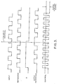
- Figure 3 the condition depicted in Figure 3 wherein the pulses in the reference pulse train are in quadrature with the pulses in the input pulse train so that the circuit is operating in its nominal or balanced condition.
- Figure 3 further illustrates conditions in the demodulator circuit when the input signal reverses polarity.
- the individual pulses in the input pulse train correspond to half cycles of sinusoidal voltage in the received signal and the Q signal represents the modulation data output from the flip-flop 17.
- the "reference” wavetrain represents the signal appearing at the output of the divider 15
- the "gated reference” represents a signal appearing at the output of the gate 5
- the "control” wavetrain represents the signal appearing at the output of the gate 1.
- the leading edge of the first reference pulse occurs when the input signal is at a high level and thus clocks the flip-flop to produce a high level signal at the Q output terminal. Since both the reference and the Q signal are now at a high level, the exclusive OR gate 5 provides a low level gated reference signal. However, since the input signal is at a high level, a high level control signal is produced by the exclusive OR gate 1. This condition persists until the termination of the first input pulse when the control signal drops to a low level because there is no input to the gate 1.
- the termination of the first reference pulse does not affect the flip-flop and the Q output remains at a high level. Since the gate 5 now receives a high level signal at only one of its terminals, a gated reference is initiated at this time. Furthermore, since the input signal applied to the gate 1 is at a low level whereas the gated reference is at a high level, a high level control signal is initiated at this time. The high level control pulse persists until the inception of the second input pulse, at which time high level signals are applied to both input terminals of the gate 1 and the output of that gate falls to a low level.
- the flip-flop 17 serves to detect the binary state of the input pulse train at each positive-going transition or leading edge of the reference pulse train. If the leading edge of a reference pulse occurs when the input signal is at a high level, a high Q signal is generated. This high Q signal persists until the leading edge of a subsequent reference pulse occurs when the input signal is at a low level whereupon the flip-flop 17 is switched and the Q output drops to a low level.
- the Q voltage remains at a high level until the polarity reversal occurs. Shortly after the polarity reversal, the reference signal switches to a high level, the flip-flop 17 effectively detects a low level input signal and the Q output drops to a low level. Since the leading edges of each of the subsequent reference pulses depicted in Figure 3 occur when the input signal is at a low level, the Q signal remains at a low level throughout the entire interval.
- the present invention is intended to operate in a biphase balanced modulation system in which the carrier, and therefore the input signal depicted in Figure 3, is transmitted with one phase when the code sequence is a binary ONE and with a 180° phase shift when the code is a binary ZERO.
- the conditions depicted prior to the polarity reversal in Figure 3 represent the transmission of a binary ONE
- the conditions depicted subsequent to the polarity reversal in the same figure would represent the transmission of a binary ZERO and the modulation data output signal Q would have high and low values, respective for these two conditions.
- the OR gate 5 serves as a selective pulse inversion means wherein the pulses in the reference pulse train are inverted and applied to the OR gate 1 when the input signal arises from the transmission of a signal having a first binary value and wherein the gate 5 serves to apply the reference signal directly to the gate 1 when the input signal arises from the transmission of a signal having the opposite binary value.
- Figure 3 depicts conditions when the circuit of the invention is in balance so that the reference signal is in phase quadrature with the input signal regardless of the binary value of the signal being transmitted.
- the phase control pulse train has a duty cycle of 50% and the resulting d.c. phase control signal applied to the reference oscillator 13 has an average value that maintains the phase of the output signal from the oscillator 13 at its "balanced" value.
- Transitory disruption of the duty cycle incident to a polarity reversal ordinarily is not significant in altering the level of the frequency control signal.
- the repetition rate of the reference pulse train can be doubled so that transition intervals can be significantly reduced.
- Figure 4 represents conditions when the circuit is unbalanced and the reference signal is no longer in phase quadrature with the input signal. Under these conditions, the various pulse trains are formed in the same manner as those appearing in Figure 3. The major difference arises in that the duty cycle of the control pulse train is no longer 50%. Under the conditions depicted in Figure 4, the reference pulse train has been advanced with respect to the input pulse train. Since the gated reference signal is synchronized with the reference signal, the gated reference is also advanced with respect to the input signal under these conditions.
- a high level control signal is produced when either one, but not both of the input and gated reference signals is at a high level.
- the control pulse train initially rises to a high level in response to the first input pulse.
- the control signal reverts to a low level since there is no gated reference pulse at that time.
- the control pulse signal soon returns to a high level in response to the occurrence of the first gated reference signal and remains at that level until the inception of the second input signal which occurs during the existence of the gated reference signal. This pattern of events is repeated until the occurrence of the polarity reversal in the input pulse train.
- the duty cycle of the control pulse train is significantly greater than the 50% duty cycle that obtain when the circuit was in balance.
- Reference to Figure 4 reveals that the duty cycle of the control pulse train remains at the same high level when the circuit has stabilized after the occurrence of the polarity reversal in the input pulse train.
- the gated reference signal prior to the polarity reversal is inverted because of the high level Q signal, whereas the gated reference signal subsequent to the polarity reversal is in phase with the reference signal.
- the duty cycle of the control pulse train and therefore the average level of the phase control signal applied to the oscillator 13 is not dependent upon the binary value of the transmitted signal.
- phase of the oscillator is temporarily altered until the reference pulse train is again in quadrature with the input pulse train at which time the circuit is in balance and the level of the phase control signal is again at its normal or balanced level.
- the control signal pulse train will be altered so that a duty cycle of less than 50% is produced.
- the phase control signal will fall to a value less than its balanced level and the phase of the oscillator 13 will be altered so as to return the phase of the signal from this oscillator to its balanced or nominal level.
- the circuit of the present invention is extremely simple. Basically, the circuit of the invention merely requires the addition of the flip-flop 17 and the exclusive OR gate 5 to a typical phase lock loop circuit.
Claims (8)
Applications Claiming Priority (2)
| Application Number | Priority Date | Filing Date | Title |
|---|---|---|---|
| US06/239,084 US4344041A (en) | 1981-02-27 | 1981-02-27 | Biphase detector |
| US239084 | 1999-01-27 |
Publications (3)
| Publication Number | Publication Date |
|---|---|
| EP0072848A1 EP0072848A1 (de) | 1983-03-02 |
| EP0072848A4 EP0072848A4 (de) | 1983-07-04 |
| EP0072848B1 true EP0072848B1 (de) | 1985-10-02 |
Family
ID=22900533
Family Applications (1)
| Application Number | Title | Priority Date | Filing Date |
|---|---|---|---|
| EP82900876A Expired EP0072848B1 (de) | 1981-02-27 | 1982-02-04 | Zweiphasendetektor |
Country Status (7)
| Country | Link |
|---|---|
| US (1) | US4344041A (de) |
| EP (1) | EP0072848B1 (de) |
| JP (1) | JPS58500344A (de) |
| CA (1) | CA1174298A (de) |
| DE (1) | DE3266597D1 (de) |
| IT (1) | IT1154296B (de) |
| WO (1) | WO1982002985A1 (de) |
Families Citing this family (10)
| Publication number | Priority date | Publication date | Assignee | Title |
|---|---|---|---|---|
| US4513427A (en) * | 1982-08-30 | 1985-04-23 | Xerox Corporation | Data and clock recovery system for data communication controller |
| US4494021A (en) * | 1982-08-30 | 1985-01-15 | Xerox Corporation | Self-calibrated clock and timing signal generator for MOS/VLSI circuitry |
| FR2535554B1 (fr) * | 1982-10-29 | 1986-04-11 | Dassault Electronique | Procede et appareil pour la reception de messages radio a signaux de type biphase |
| US4532637A (en) * | 1983-01-03 | 1985-07-30 | Sperry Corporation | Differential receiver |
| US4453165A (en) * | 1983-01-03 | 1984-06-05 | Sperry Corporation | Differential Doppler receiver |
| US4547738A (en) * | 1983-06-10 | 1985-10-15 | American Standard Inc. | Phase shift demodulator |
| GB8506100D0 (en) * | 1985-03-08 | 1985-04-11 | Int Computers Ltd | Decoder |
| US4905257A (en) * | 1988-08-31 | 1990-02-27 | Unisys Corporation | Manchester decoder using gated delay line oscillator |
| US5394115A (en) * | 1994-04-01 | 1995-02-28 | Conifer Corporation | Automatic sweep acquisition circuit for a phase-locked-loop |
| US6388717B1 (en) * | 1999-01-20 | 2002-05-14 | Harris Corporation | Digital television transmitting system having data and clock recovering circuit |
Family Cites Families (5)
| Publication number | Priority date | Publication date | Assignee | Title |
|---|---|---|---|---|
| US3979746A (en) * | 1975-04-28 | 1976-09-07 | The United States Of America As Represented By The Secretary Of The Navy | High-speed Manchester code demodulator |
| US3991378A (en) * | 1975-06-30 | 1976-11-09 | Rockwell International Corporation | Electronic phaselock circuitry |
| US4167760A (en) * | 1978-03-28 | 1979-09-11 | Ampex Corporation | Bi-phase decoder apparatus and method |
| JPS556964A (en) * | 1978-06-30 | 1980-01-18 | Toshiba Corp | Carrier wave reproducing device |
| IT1158893B (it) * | 1978-07-28 | 1987-02-25 | Sits Soc It Telecom Siemens | Disposizione circuitale per la generazione degli impulsi di campionamento di particolare applicazione nella stazione ricevente di un sistema per la trasmissione di dati |
-
1981
- 1981-02-27 US US06/239,084 patent/US4344041A/en not_active Expired - Fee Related
-
1982
- 1982-01-27 CA CA000394994A patent/CA1174298A/en not_active Expired
- 1982-02-04 WO PCT/US1982/000151 patent/WO1982002985A1/en active IP Right Grant
- 1982-02-04 EP EP82900876A patent/EP0072848B1/de not_active Expired
- 1982-02-04 DE DE8282900876T patent/DE3266597D1/de not_active Expired
- 1982-02-04 JP JP57500915A patent/JPS58500344A/ja active Pending
- 1982-02-19 IT IT47836/82A patent/IT1154296B/it active
Non-Patent Citations (1)
| Title |
|---|
| ELECTRONICS, vol. 46, no. 23, November 8, 1973 NEW YORK (US) C.A. HERBST: "Digital demodulator for phase-shift-keyed data", page 94 * |
Also Published As
| Publication number | Publication date |
|---|---|
| JPS58500344A (ja) | 1983-03-03 |
| EP0072848A4 (de) | 1983-07-04 |
| US4344041A (en) | 1982-08-10 |
| WO1982002985A1 (en) | 1982-09-02 |
| EP0072848A1 (de) | 1983-03-02 |
| DE3266597D1 (de) | 1985-11-07 |
| CA1174298A (en) | 1984-09-11 |
| IT1154296B (it) | 1987-01-21 |
| IT8247836A0 (it) | 1982-02-19 |
Similar Documents
| Publication | Publication Date | Title |
|---|---|---|
| CA1067152A (en) | Digital timing recovery | |
| US3997847A (en) | Digital demodulator for differentially encoded phase-shift-keyed data | |
| EP0008491B1 (de) | Digitaler Demodulator für phasenumgetastete Signale | |
| US3818347A (en) | Receiver for amplitude modulated quadrature carrier signals | |
| EP0072848B1 (de) | Zweiphasendetektor | |
| US4580101A (en) | FM demodulators with local oscillator frequency control circuits | |
| US4575684A (en) | Differential phase shift keying receiver | |
| EP0259867B1 (de) | Demodulator für PSK-modulierte Signale | |
| US5347228A (en) | BPSK demodulator using compound phase-locked loop | |
| US5506873A (en) | Demodulator for a phase shift keying (PSK) signal | |
| EP0258697B1 (de) | FSK-Signal-Demodulator | |
| EP0412291B1 (de) | Quadraturempfänger für FSK-Signale mit Frequenzverschiebungskompensation | |
| US4656431A (en) | Digital frequency discriminator | |
| CA2262882C (en) | Frequency lock indicator for fpll demodulated signal having a pilot | |
| GB2137836A (en) | FM Demodulators | |
| US4744094A (en) | BPSK demodulator with D type flip/flop | |
| EP0257301B1 (de) | PSK-System und -Modem | |
| US4870660A (en) | Variable frequency rate receiver | |
| EP0151394B1 (de) | Demodulator für digitale, frequenzmodulierte Signale | |
| JPS6323448A (ja) | 変復調方式 | |
| US4618830A (en) | PSK demodulator using asynchronous local oscillator | |
| JPH01194552A (ja) | 位相誤差信号発生回路配置 | |
| US6163208A (en) | One bit digital phase shift keyed carrier recovery and demodulator circuit | |
| CA1269724A (en) | Phase-locked loop circuit | |
| JPH0515336B2 (de) |
Legal Events
| Date | Code | Title | Description |
|---|---|---|---|
| PUAI | Public reference made under article 153(3) epc to a published international application that has entered the european phase |
Free format text: ORIGINAL CODE: 0009012 |
|
| 17P | Request for examination filed |
Effective date: 19821011 |
|
| AK | Designated contracting states |
Designated state(s): BE DE FR GB NL SE |
|
| GRAA | (expected) grant |
Free format text: ORIGINAL CODE: 0009210 |
|
| AK | Designated contracting states |
Designated state(s): BE DE FR GB NL SE |
|
| REF | Corresponds to: |
Ref document number: 3266597 Country of ref document: DE Date of ref document: 19851107 |
|
| ET | Fr: translation filed | ||
| PLBE | No opposition filed within time limit |
Free format text: ORIGINAL CODE: 0009261 |
|
| STAA | Information on the status of an ep patent application or granted ep patent |
Free format text: STATUS: NO OPPOSITION FILED WITHIN TIME LIMIT |
|
| 26N | No opposition filed | ||
| PGFP | Annual fee paid to national office [announced via postgrant information from national office to epo] |
Ref country code: SE Payment date: 19890130 Year of fee payment: 8 |
|
| PGFP | Annual fee paid to national office [announced via postgrant information from national office to epo] |
Ref country code: BE Payment date: 19890421 Year of fee payment: 8 |
|
| PG25 | Lapsed in a contracting state [announced via postgrant information from national office to epo] |
Ref country code: SE Effective date: 19900205 |
|
| PG25 | Lapsed in a contracting state [announced via postgrant information from national office to epo] |
Ref country code: BE Effective date: 19900228 |
|
| BERE | Be: lapsed |
Owner name: SPERRY CORP. Effective date: 19900228 |
|
| PGFP | Annual fee paid to national office [announced via postgrant information from national office to epo] |
Ref country code: FR Payment date: 19911227 Year of fee payment: 11 |
|
| PGFP | Annual fee paid to national office [announced via postgrant information from national office to epo] |
Ref country code: GB Payment date: 19920120 Year of fee payment: 11 |
|
| PGFP | Annual fee paid to national office [announced via postgrant information from national office to epo] |
Ref country code: DE Payment date: 19920226 Year of fee payment: 11 |
|
| PGFP | Annual fee paid to national office [announced via postgrant information from national office to epo] |
Ref country code: NL Payment date: 19920229 Year of fee payment: 11 |
|
| PG25 | Lapsed in a contracting state [announced via postgrant information from national office to epo] |
Ref country code: GB Effective date: 19930204 |
|
| PG25 | Lapsed in a contracting state [announced via postgrant information from national office to epo] |
Ref country code: NL Effective date: 19930901 |
|
| GBPC | Gb: european patent ceased through non-payment of renewal fee |
Effective date: 19930204 |
|
| NLV4 | Nl: lapsed or anulled due to non-payment of the annual fee | ||
| PG25 | Lapsed in a contracting state [announced via postgrant information from national office to epo] |
Ref country code: FR Effective date: 19931029 |
|
| PG25 | Lapsed in a contracting state [announced via postgrant information from national office to epo] |
Ref country code: DE Effective date: 19931103 |
|
| REG | Reference to a national code |
Ref country code: FR Ref legal event code: ST |
|
| EUG | Se: european patent has lapsed |
Ref document number: 82900876.2 Effective date: 19901107 |