EP0071663A2 - Integrated circuit for the regulation of the power supply voltage according to the switching principle in television apparatuses - Google Patents
Integrated circuit for the regulation of the power supply voltage according to the switching principle in television apparatuses Download PDFInfo
- Publication number
- EP0071663A2 EP0071663A2 EP81106182A EP81106182A EP0071663A2 EP 0071663 A2 EP0071663 A2 EP 0071663A2 EP 81106182 A EP81106182 A EP 81106182A EP 81106182 A EP81106182 A EP 81106182A EP 0071663 A2 EP0071663 A2 EP 0071663A2
- Authority
- EP
- European Patent Office
- Prior art keywords
- input
- counter
- output
- voltage
- flop
- Prior art date
- Legal status (The legal status is an assumption and is not a legal conclusion. Google has not performed a legal analysis and makes no representation as to the accuracy of the status listed.)
- Granted
Links
Images


Classifications
-
- H—ELECTRICITY
- H02—GENERATION; CONVERSION OR DISTRIBUTION OF ELECTRIC POWER
- H02M—APPARATUS FOR CONVERSION BETWEEN AC AND AC, BETWEEN AC AND DC, OR BETWEEN DC AND DC, AND FOR USE WITH MAINS OR SIMILAR POWER SUPPLY SYSTEMS; CONVERSION OF DC OR AC INPUT POWER INTO SURGE OUTPUT POWER; CONTROL OR REGULATION THEREOF
- H02M3/00—Conversion of DC power input into DC power output
- H02M3/22—Conversion of DC power input into DC power output with intermediate conversion into AC
- H02M3/24—Conversion of DC power input into DC power output with intermediate conversion into AC by static converters
- H02M3/28—Conversion of DC power input into DC power output with intermediate conversion into AC by static converters using discharge tubes with control electrode or semiconductor devices with control electrode to produce the intermediate AC
- H02M3/325—Conversion of DC power input into DC power output with intermediate conversion into AC by static converters using discharge tubes with control electrode or semiconductor devices with control electrode to produce the intermediate AC using devices of a triode or a transistor type requiring continuous application of a control signal
- H02M3/335—Conversion of DC power input into DC power output with intermediate conversion into AC by static converters using discharge tubes with control electrode or semiconductor devices with control electrode to produce the intermediate AC using devices of a triode or a transistor type requiring continuous application of a control signal using semiconductor devices only
- H02M3/33507—Conversion of DC power input into DC power output with intermediate conversion into AC by static converters using discharge tubes with control electrode or semiconductor devices with control electrode to produce the intermediate AC using devices of a triode or a transistor type requiring continuous application of a control signal using semiconductor devices only with automatic control of the output voltage or current, e.g. flyback converters
- H02M3/33515—Conversion of DC power input into DC power output with intermediate conversion into AC by static converters using discharge tubes with control electrode or semiconductor devices with control electrode to produce the intermediate AC using devices of a triode or a transistor type requiring continuous application of a control signal using semiconductor devices only with automatic control of the output voltage or current, e.g. flyback converters with digital control
Definitions
- the invention relates to integrable circuit arrangements for regulating DC supply voltages according to the switching regulator principle in television sets, a power semiconductor component being periodically switched on and off by a signal which is pulse-width-modulated as a function of a nominal / actual comparison which is synchronized line-by-line during each line duration, cf. . the preamble of claim 1.
- Switching regulators of this type for general use with a pulse-width-modulated control signal for the power semiconductor component which is to be switched on and off periodically are already known in an integrated form, cf. for example the magazine "Electronic Design", February 1, 1979, pp. 102 and 18 January 1980, pp. 94-101.
- the switching regulators shown generate the pulse-width-modulated control signal in the manner of analog circuits, i.e. that is, depending on the actual / target comparison, the pulse width can be changed continuously.
- a sawtooth generator is also provided, which serves as a reference voltage when generating the pulse-width-modulated control signal. This sawtooth generator has a synchronizing input in the second reference.
- DE-OS 28 43 988 it is known from DE-OS 28 43 988 to also build control circuits based on the switching regulator principle in such a way that the pulse-width-modulated control signal is generated on the basis of digital circuit principles.
- a microprocessor is used for this purpose, which, starting from a clock signal, generates the pulse-width-modulated signal in steps of this clock frequency.
- the object of the invention is therefore to develop the integrated switching regulators known from the magazine "Electronic Design” using the digital principles obtained from the aforementioned DE-OS in such a way that they are suitable for use in television sets.
- those partial aspects of the arrangement according to DE-OS are to be used which are applicable in the sense of solving this task.
- no element protection is claimed for this.
- the solution to the problem thus consists in measures known in part from DE-OS and the other means specified in the characterizing part of claim 1. To solve the task, is therefore from using a microprocessor.
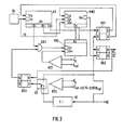
- Fig. 1 the construction of a television power supply unit using a switching regulator, which is conventional in principle, is shown.
- the essential parts of this basic circuit diagram are provided with reference numerals.
- the mains voltage U N is applied to the primary winding of a main transformer via a rectifier bridge and the power semiconductor component TL.
- Another small transformer feeds another rectifier, from which the operating voltage for the switching regulator is taken.
- the network side is completely galvanically isolated from the DC voltage side, as required by the VDE standards.
- the semiconductor component TL ' is shown, which is controlled by the pulse width modulator PWM and acts on the power semiconductor component TL in a known manner via the associated further transformer.
- known flyback converter principle generates corresponding AC voltages, which result in rectified, the regulated voltages U g and U gg .
- the voltage proportional to this becomes removed and fed to the pulse width modulator PWM as information about the actual value.
- the load current I L flowing in the load circuit is measured by means of the current measuring resistor RI1 and the voltage drop resulting therefrom is also supplied to the pulse width modulator as current information U.
- the tap for the current signal U. ie the connection point between the secondary windings and the current measuring resistor RI1, is connected to the regulated voltage U g via the resistor RI2, so that this connection point is fixed in terms of potential.
- FIG. 1 also shows the clock generator TG, the output signal of which is fed to the pulse width modulator PWM as a clock signal TS, as well as the horizontal synchronizing pulses HZ originating from the synchronizing signal separation stage SS of the television set.
- a clock oscillator for example, is a quartz oscillator with four times the color subcarrier frequency of color television sets, an oscillator with an oscillation frequency of 17.7 MHz.
- the setpoint / actual comparison is carried out by the first digital comparator stage KS1, at the first input of which the reference voltage U ref and at the second input of which the voltage U 9 proportional to the regulated voltage U 9 according to FIG. 1 is present.
- the reference voltage U ref can be generated in any of the known ways, for example by means of a Z-diode or a temperature-compensated Z-diode.
- the first digital comparator KS1 produces at its output only a binary signal, the two values, that is, a positive voltage value assigned to H-level, and a one to lower voltage value associated with the L level, the two input si g nal Schemeen U ref> or U ref ⁇ assigned.
- control amplifier used in conventional analog control circuits is replaced by the comparator stage, which only supplies a binary signal regarding the fact that the reference voltage U ref falls below or exceeds the actual value in the form of the voltage U '.
- the further digital comparator stages to be added in the further exemplary embodiments and further developments are also stages of this type with a binary signal output.
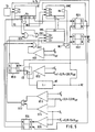
- the clock generator TG is connected to the counting input Ez of the up counter VZ of the counting capacitance n and to the counting input Ez of the preselection counter VWZ.
- the pulses of the clock signal TS are therefore counted by means of these two counters during certain times to be described.
- the counter reading output Azg is at the counter input Ez of the up / down counter, which thus counts these output pulses of the up counter VZ either in the up or down direction, the output signal of the first comparator stage KS1 defining the counting direction via the changeover input Evr for up or down counting.
- the counter outputs Az of the up / down counter VRZ are connected in parallel to the preselection inputs Ev of the preselection counter VWZ, which is indicated by the band-like arrow in FIG. 2.
- the counter reading reached at certain times in the up / down counter VRZ is thus read into the preselection counter VWZ and is used there to determine the duration of a counting cycle.
- the preselection counter VWZ can either be an up counter that counts from the preselected counter reading up to a certain higher counter reading and then emits an impulse at this counter reading output as a zero crossing output, or it can be a down counter that counts down to zero from the preselected counter reading and then delivers a zero crossing output pulse.
- the take-over input Eu of the preselection counter VWZ is at one of the other counter reading outputs, namely the output Azk, of the up-counter VZ. If this counter has thus reached the counter reading k, the counter reading reached in the up / down counter at this point in time is adopted as the preselection counter reading in the preselection counter VWZ.
- the nth counter output Azn of the up counter VZ is connected to the R input of the first RS flip-flop RS1, the Q output of which lies at the start and enable input Es of the up-counter VZ, while the Q output is connected to the start and enable input Es of the preselection counter VWZ.
- the horizontal synchronizing pulses HZ are located at the S input of the first RS flip-flop RS1.
- the first RS flip-flop RS1 is set, and the up counter VZ is started by the corresponding Q signal.
- the first RS flip-flop RS1 is reset again, so that on the one hand the up counter VZ cannot continue counting but on the other hand the preset counter VWZ is now started via the Q signal.
- the zero crossing output of the preselection counter VWZ is connected to the R input of the second RS flip-flop RS2, at whose S input the horizontal pulses HZ are connected.
- This flip-flop like the flip-flop RS1, is therefore set by each horizontal pulse and is reset when the preselection counter VWZ reaches zero.
- a pulse which is the pulse width modulated pulse for driving the Leistun g .leiterbauelements TL is formed.
- This drive pulse is thus composed in time of a first part, which is predetermined by the counting capacity n of the up-counter VZ, and of a second part, which is determined by the counter reading given at the time of transfer by the counter reading of the up / down counter.
- the pulse width modulated The signal therefore has a minimum pulse width specified by the up-counter VZ and a maximum pulse width which is determined by the counting capacities of the up-counter VZ and the up / down counter VRZ.
- the counting capacities of the three counters VZ, VWZ, VRZ are selected taking into account the frequency of the clock generator TG and the line duration so that the maximum pulse width of the pulse width modulated signal covers a certain part of the line duration, e.g. B. 44 ⁇ s, does not exceed.
- FIG. 3 shows a further development of the arrangement according to FIG. 2, which contains additional circuit parts for the start-up phase of the switching regulator after the mains voltage has been switched on.
- the second digital comparator stage KS2 is provided, which measures the voltage with a reference voltage compares, which is approximately 0.75 to 0.95 times the reference voltage U ref . So is the voltage proportional to the regulated voltage U 9 5 to 25% below their nominal value, the second comparator stage KS2 emits one binary signal level and above this range the other binary signal level.
- These two signal levels control the changeover contact of the electronic switch ES, the output of which is at the S input of the third RS flip-flop RS3.
- At one input of the switch ES are the horizontal synchronizing pulses HZ and at the other the output of the frequency divider BT, the input of which is also supplied with the horizontal synchronizing pulses HZ.
- the R input of the third RS flip-flop RS3 is connected to the Q output of the second RS flip-flop RS2 and is therefore supplied with the pulse-width-modulated pulse.
- the Q output The third RS flip-flop RS3 is located at an input of the first AND gate UG1, which is inserted with its other input-output path into the connecting line between the counter reading output Azg of the up-counter VZ and the counting input Ez of the up / down counter VRZ.
- the third RS flip-flop RS3 is set by the number of horizontal pulses reduced by the divider factor of the frequency divider BT.
- the counting pulses to the up / down counter are passed through the first AND gate UG1.
- the change in its counter reading Az thus takes place much more slowly, ie the pulse-width-modulated signal is not changed during the start-up phase for the duration of each line, but only during every r-th line if the divisor of the frequency divider BT is designated by r.
- FIG. 4 shows a further development of the arrangement according to FIG. 3, which relates to the additional circuit parts compared to FIG. 3, the third digital comparator stage KS3 and the first OR gate OG1.
- These two too Additional circuit parts can, however, also be provided in the arrangement according to FIG. 2, ie without the additional circuit parts in FIG. 3. They relate to the measuring circuit short-circuit protection of the control circuit and can therefore also be used regardless of the use of the start-up circuit according to FIG.
- the third comparator stage KS3 compares the voltage proportional to the regulated voltage U g with the fixed voltage U of a first voltage threshold, which is approximately 0.1 to 0.2 times the reference voltage U ref .
- the output signal of the third comparator stage KS3 is fed to the up / down counter VRZ now equipped with the reset input Er and also via the first OR gate OG1 also to the R input of the second RS flip-flop RS2.
- the other input-output path of the first OR gate OG1 is inserted into the connecting line between the zero crossing output An of the preselection counter VWZ and the R input of the second RS flip-flop RS2.
- the output signal of the third comparator stage KS3 resets the up / down counter to its zero position and thus ensures that the preset counter also returns to its zero position after the next transfer pulse reached.
- this output pulse from the third comparator stage KS3 also resets the second RS flip-flop RS2, which determines the duration of the pulse-width-modulated signal, and the output pulse duration is thereby immediately reduced to the minimum duration.
- This type of control loop protection is effective immediately after the short circuit occurs and is also maintained for the duration of the short circuit. Furthermore, the short-circuit protection automatically becomes ineffective after the short circuit has ceased to exist, that is to say the operation of a so-called electronic fuse with automatic reclosure is present.
- FIG. 5 shows a further development of the arrangement according to FIG. 4, which in addition to the control loop protection also represents protection in the event of a short circuit and current overload of the power supply unit output voltage.
- the additional circuit parts compared to FIG. 4 are provided, namely the fourth and fifth digital comparator stages KS4 and KS5, the fourth RS flip-flop RS4, the second and the third OR gate OG2, OG3 and the second and the third AND gate UG2, UG3.
- the second OR gate OG2 can be omitted if the control loop protection is not provided by means of the third comparator stage KS3.
- the fourth and fifth comparator stages KS4, KS5 compare the fixed voltage U of the first voltage threshold and the fixed voltage, respectively a second voltage threshold each with the load current proportional voltage U i , cf. Fig. 1.
- the fixed tension the second voltage threshold is 0.25 to 0.4 times the reference voltage U ref .
- the output of the fourth comparator stage KS4 is OR-linked to that of the third comparator stage KS3 via the second OR gate OG2 and thus leads to the reset input Er of the up / down counter VRZ. So the load current exceeds one of the second voltage threshold If the value is correct, the control is immediately reduced to the minimum pulse width of the pulse-width-modulated signal, as in the short-circuit case of the control loop described above.
- the fifth comparator stage KS5 is used in a load current range between the maximum load current specified by the first voltage threshold U s and that by the second voltage threshold predetermined load current achieved a gradual reduction in the pulse width of the pulse width modulated signal.
- the fifth comparator stage KS5 compares the fixed voltage value the second voltage threshold with the load current-dependent voltage U i .
- the output of the fifth comparator stage KS5 is connected to the S input of the fourth RS flip-flop RS4, the R input of which is connected to the Q output of the first RS flip-flop RS1.
- the Q output of the fourth RS flip-flop RS4 is connected to one input of the second AND gate UG2, the other input of which is connected to a further counter output Azj of the up-counter VZ and the output of which is connected to an input of the third OR gate OG3. This is inserted with its other input-output path into the connecting line between the output of the first AND gate UG1 and the counting input Ez of the up / down counter.
- the counting input Ez of the up / down counter VRZ is supplied with the additional pulse at the counter reading output Azj of the upstream counter VZ in addition to the output pulse at the counter reading output Azg. ie the Up / down counter is counted at double frequency in the reverse direction. In each line, the pulse width reduction rate is twice as high as in normal control mode.
- the Q output of the fourth RS flip-flop RS4 is AND-linked to the output signal of the first comparator stage KS1 by means of the third AND gate UG3. that is, regardless of the output signal of the comparator stage KS1, the up / down counter VRZ can count only as long as a current exceeding proportional to the U1 threshold is determined by the comparator stage KS5.
- the invention is thus specifically designed to meet the requirements of a switching regulator in a television set. It can be adapted to a wide variety of accidents, particularly when using the explained further developments. Due to the principle on which the invention is based, the division of the pulse duration of the pulse-width-modulated signal into a minimum pulse duration and a variable, it is always ensured that each fault, depending on its severity, leads to a reduction in the instantaneous pulse width either immediately or at twice the rate of change.
- white can also be used tere functions of the power supply are realized, such as a shutdown of the power supply after a certain number of malfunctions or an electronic on / off switch.
- the maximum pulse width of the pulse-width-modulated signal is 44.8 microseconds and the minimum pulse width is 1.5 microseconds, while the pulse width in the adjusted state is 26 to 32 microseconds.
- the switch-off delay after the protective circuits described have responded is 1 ⁇ s.
- the circuit according to the invention is suitable due to the fact that it works with exclusively digital subcircuits, in particular for integration by means of insulating layer field effect transistors, that is to say for integration in the so-called MOS technology.
- bipolar integration techniques which are particularly suitable for digital circuits, for example the technique of the so-called integrated injection logic (I 2 L circuits) or the implementation using other bipolar digital circuit families.
- the change steepness in the start-up range is +56 ns per 32 lines.
- the rate of change of the load current limitation is -112 ns per line.
Landscapes
- Engineering & Computer Science (AREA)
- Power Engineering (AREA)
- Dc-Dc Converters (AREA)
Abstract
Dabei wird ein Leistungshalbleiterbauelement (TL) von einem Signal, das in Abhängigkeit von einem während jeder Zeilendauer zeilensynchron erfolgenden Soll/Ist-Vergleich pulsbreitenmoduliert ist, periodisch ein- und ausgeschaltet. Das pulsbreitenmodulierte Signal ist mittels Digitalschaltungen, ausgehend von der Periodendauer eines Taktsignals (TS), erzeugt und in Schritten dieser Periodendauer variabel. Dem Soll/Ist-Vergleich dient eine digitale Komparatorstufe (KS1), an deren erstem Eingang eine Referenzspannung (Uref) und an deren zweitem Eingang eine der geregelten Spannung (Ug) proportionale Spannung (U'9) liegt und an deren Ausgang lediglich ein Binärsignal entsteht, dessen beide Werte den beiden Eingangssignalbereichen Uref>U'g bzw. Uref<U'g zugeordnet sind. Der Taktsignalgenerator (TG) ist am Zähleingang (Ez) eines Vorwärtszählers (VZ) der Zähikapazität n und am Zähleingang (Ez) eines Vorwahlzählers (VWZ) angeschiossen. Einer (Azg) der Zähierstandausgänge des Vorwärtszählers (VZ) ist mit dem Zähleingang (Ez) eines Vorwärts/ Rückwärtszählers (VRZ) verbunden, dessen Umschaiteingang (Evr) auf Vor- oder Rückwärtszählen am Ausgang der Komparatorstufe (KS1) und dessen Zähierstandausgänge (Az) an den Vorwahleingängen (Ev) des Vorwahlzählers (VWZ) liegen, dessen Übernahmeeingang (En) an einem (Azk) der anderen Zählerstandausgänge des Vorwärtszählers (VZ) liegt. Der R-Eingang eines ersten RS-Flipflops (RS1) liegt am n-ten Zählerstandausgang (Azn) des Vorwärtszählers (VZ) und dessen Q-Ausgang am Starteingang (Es) des Vorwärtszählers (VZ), während dessen 
Description
Die Erfindung betrifft integrierbare Schaltungsanordnungen zur Regelung von Versorgungsgleichspannungen nach dem Schaltregler-Prinzip in Fernsehgeräten, wobei ein Leistungshalbleiterbauelement von einem Signal, das in Abhängigkeit von einem während jeder Zeilendauer zeilensynchron erfolgenden Soll/Ist-Vergleich pulsbreitenmoduliert ist, periodisch ein- und ausgeschaltet wird, vgl. den Oberbegriff des Anspruchs 1.The invention relates to integrable circuit arrangements for regulating DC supply voltages according to the switching regulator principle in television sets, a power semiconductor component being periodically switched on and off by a signal which is pulse-width-modulated as a function of a nominal / actual comparison which is synchronized line-by-line during each line duration, cf. . the preamble of
Schaltregler dieser Art für allgemeine Verwendung mit pulsbreitenmoduliertem Steuersignal für das periodisch ein- und auszuschaltende Leistungshalbleiterbauelement sind in integrierter Form bereits bekannt, vgl. beispielsweise die Zeitschrift "Electronic Design", 1. Februar 1979, S. 102 und 18. Januar 1980, S. 94-101. Die gezeigten Schaltregler erzeugen das pulsbreitenmodulierte Steuersignal nach Art analoger Schaltungen, d. h., in Abhängigkeit vom Ist/Soll-Vergleich ist die Pulsbreite kontinuierlich veränderbar. Bei den bekannten Schaltungen ist ferner jeweils ein Sägezahngenerator vorgesehen, der als Vergleichsspannung bei der Erzeugung des pulsbreitenmodulierten Steuersignals dient. Dieser Sägezahngenerator hat in der zweitgenannten Literaturstelle einen Synchronisiereingang.Switching regulators of this type for general use with a pulse-width-modulated control signal for the power semiconductor component which is to be switched on and off periodically are already known in an integrated form, cf. for example the magazine "Electronic Design", February 1, 1979, pp. 102 and 18 January 1980, pp. 94-101. The switching regulators shown generate the pulse-width-modulated control signal in the manner of analog circuits, i.e. that is, depending on the actual / target comparison, the pulse width can be changed continuously. In the known circuits, a sawtooth generator is also provided, which serves as a reference voltage when generating the pulse-width-modulated control signal. This sawtooth generator has a synchronizing input in the second reference.
Andererseits ist es aus der DE-OS 28 43 988 bekannt, Regelschaltungen nach dem Schaltregler-Prinzip auch so aufzubauen, daß das pulsbreitenmodulierte Steuersignal aufgrund digitaler Schaltungsprinzipien erzeugt wird. Hierzu dient im wesentlichen ein Mikroprozessor, der, ausgehend von einem Taktsignal, das pulsbreitenmodulierte Signal in Schritten dieser Taktfrequenz erzeugt.On the other hand, it is known from DE-OS 28 43 988 to also build control circuits based on the switching regulator principle in such a way that the pulse-width-modulated control signal is generated on the basis of digital circuit principles. A microprocessor is used for this purpose, which, starting from a clock signal, generates the pulse-width-modulated signal in steps of this clock frequency.
Sollen derartige Schaltregler in Fernsehgeräten verwendet werden, so sind spezielle Forderungen zu erfüllen. Als Hauptforderung ist dabei anzusehen, daß die Regelgeschwindigkeit, mit der eine Regelabweichung zu einer Nachregelung führt, so groß sein muß, daß dies innerhalb der Dauer des Horizontalablenkimpulses, also der Zeilendauer, erfolgt. Bei der Anordnung nach der genannten DE-OS ist die Einstellgeschwindigkeit wesentlich niedriger, da aufgrund der Verwendung des Mikroprozessors eine wesentlich längere Signalverarbeitungszeit vorgegeben ist.If such switching regulators are to be used in television sets, special requirements have to be met. The main requirement is that the control speed with which a control deviation leads to readjustment must be so great that this takes place within the duration of the horizontal deflection pulse, ie the line duration. In the arrangement according to the above-mentioned DE-OS, the setting speed is considerably lower, since the use of the microprocessor means that the signal processing time is much longer.
Die Aufgabe der Erfindung besteht daher darin, die aus der Zeitschrift"Electronic Design" bekannten integrierten Schaltregler unter Anwendung der aus der genannten DE-OS bekamiten digitalen Prinzipien so weiterzubilden, daß sie für den Betrieb in Fernsehgeräten geeignet sind. Dabei soll auf diejenigen Teilaspekte der Anordnung nach der DE-OS zurückgegriffen werden, die im Sinne der Lösung dieser Aufgabe anwendbar sind. Soweit diese teilweise bekannten Merkmale im Kennzeichenteil des Anspruchs 1 erwähnt sind, wird hierfür kein Elementenschutz beansprucht. Die Lösung der gestellten Aufgabe besteht also in zum Teil aus der DE-OS bekannten Maßnahmen und den weiteren im Kennzeichen des Anspruchs 1 angegebenen Mitteln. Zur Lösung der gestellten Aufgabe wird also von der Verwendung eines Mikroprozessors abgegangen. Vielmehr werden nur solche digitalen Grundschaltungen, wie Zähler und Verknüpfungsglieder, verwendet, die in ihrer speziellen schaltungstechnischen Verknüpfung die spezielle Regelaufgabe zu lösen und insbesondere das impulsbreitenmodulierte Steuersignal zu erzeugen geeignet sind, wobei in jeder Zeile des Fernsehbildes sowohl die Regelabweichung ermittelt als auch die daraus resultierende Regelung ausgeführt wird.The object of the invention is therefore to develop the integrated switching regulators known from the magazine "Electronic Design" using the digital principles obtained from the aforementioned DE-OS in such a way that they are suitable for use in television sets. In this case, those partial aspects of the arrangement according to DE-OS are to be used which are applicable in the sense of solving this task. Insofar as these partially known features are mentioned in the characterizing part of
Die in den Unteransprüchen gekennzeichneten Weiterbildungen der Erfindung erweitern das im Anspruch 1 niedergelegte Prinzip der Erfindung durch die bei Regelschaltungen bekannten zusätzlichen Funktionen der sogenannten elektronischen Sicherung, also des Abschaltens des Reglers bzw. des Zurückregelns in einen ungefährlichen Belastungsbereich, wenn im Lastkreis ein Kurzschluß oder eine Überlastung auftritt. Diese zusätzlichen Funktionen sind dabei jedoch ebenfalls wie die Grundfunktionen mittels digitaler Schaltungs- und Funktionsprinzipien realisiert und unterscheiden sich somit von der nach analogen Prinzipien arbeitenden Realisierung bei den bekannten Anordnungen.The developments of the invention characterized in the subclaims expand the principle of the invention as set out in
Der Gegenstand der Erfindung und dessen Weiterbildungen werden nun anhand der Figuren der Zeichnung näher erläutert.
- Fig. 1 zeigt in Form eines Prinzipschaltbilds ein Fernsehgerät-Netzteil unter Verwendung der Schaltungsanordnung'nach der Erfindung,
- Fig. 2 zeigt in Form eines Blockschaltbilds den Grundaufbau des der Erfindung zugrundeliegenden Prinzips,
- Fig. 3 zeigt eine Weiterbildung der Anordnung nach Fig. 2 für den Anlaufbetrieb nach Einschalten der Netzspannung,
- Fig. 4 zeigt eine Weiterbildung der Anordnung nach Fig. 3 mit Kurzschlußschutz im Meßkreis, und
- Fig. 5 zeigt eine Weiterbildung der Anordnung nach Fig. 4 mit einer Erweiterung für den erwähnten Schutz bei Überlastung und Kurzschluß im Lastkreis.
- 1 shows, in the form of a basic circuit diagram, a television power pack using the circuit arrangement according to the invention,
- Fig. 2 shows the reason in the form of a block diagram construction of the principle on which the invention is based,
- 3 shows a development of the arrangement according to FIG. 2 for the start-up operation after switching on the mains voltage,
- Fig. 4 shows a development of the arrangement of FIG. 3 with short-circuit protection in the measuring circuit, and
- 5 shows a development of the arrangement according to FIG. 4 with an extension for the protection mentioned in the event of overload and short circuit in the load circuit.
In Fig. 1 ist der vom Prinzip her übliche Aufbau eines Fernsehgerät-Netzteils unter Verwendung eines Schaltreglers gezeigt. Für die Zwecke der Erfindung sind die wesentlichen Teile dieses Prinzipschaltbilds mit Bezugszeichen versehen. So wird die Netzspannung UN über eine Gleichrichterbrücke und das Leistungshalbleiterbauelement TL an die Primärwicklung eines Haupttransformators gelegt. Ein weiterer kleiner Transformator speist einen weiteren Gleichrichter, dem die Betriebsspannung für den Schaltregler entnommen wird. Wie durch die gestrichelten Linien zum Ausdruck kommt, ist die Netz-Seite vollständig von der Gleichspannungsseite galvanisch getrennt, wie dies von den VDE-Normen gefordert wird.In Fig. 1, the construction of a television power supply unit using a switching regulator, which is conventional in principle, is shown. For the purposes of the invention, the essential parts of this basic circuit diagram are provided with reference numerals. Thus, the mains voltage U N is applied to the primary winding of a main transformer via a rectifier bridge and the power semiconductor component TL. Another small transformer feeds another rectifier, from which the operating voltage for the switching regulator is taken. As is shown by the dashed lines, the network side is completely galvanically isolated from the DC voltage side, as required by the VDE standards.
Auf der netzgetrennten Seite ist das Halbleiterbauelement TL' gezeigt, das vom Pulsbreitenmodulator PWM angesteuert wird und über den zugeordneten weiteren Transformator auf das erwähnte Leistungshalbleiterbauelement TL in bekannter Weise einwirkt. Dadurch werden in den beiden gezeigten Sekundärwicklungen nach dem von Gleichspannungskonvertern her bekannten Sperrwandler-Prinzip entsprechende Wechselspannungen erzeugt, die gleichgerichtet die geregelten Spannungen Ug und Ugg ergeben. Am Abgriff des zwischen dem auf das Fernsehgerät-Chassis bezogenen Schaltungsnullpunkt und der geregelten Spannung Ug liegenden Spannungsteilers RG1, RG2 wird die hierzu proportionale Spannung ![]()
![]()
In Fig. 1 ist ferner der Taktgenerator TG gezeigt, dessen Ausgangssignal als Taktsignal TS dem Pulsbreitenmodulator PWM zugeführt ist, ebenso wie die aus der Synchronsignal-Abtrennstufe SS des Fernsehgeräts stammenden Horizontal-Synchronimpulse HZ.1 also shows the clock generator TG, the output signal of which is fed to the pulse width modulator PWM as a clock signal TS, as well as the horizontal synchronizing pulses HZ originating from the synchronizing signal separation stage SS of the television set.
In Fig. 2 ist das Grundprinzip des Pulsbreitenmodulators PWM nach Fig. 1 in Form eines schematischen Blockschaltbilds gezeigt. Das pulsbreitenmodulierte Signal wird mittels Digitalschaltungen, ausgehend von der Periodendauer des Taktsignals, erzeugt und ist in Schritten dieser Periodendauer variabel. Als Taktgenerator TG eignet sich beispielsweise ein Quarzoszillator mit der vierfachen Farbhilfsträgerfrequenz von Farbfernsehgeräten, also ein Oszillator mit einer Schwingfrequenz von 17,7 MHz.2 shows the basic principle of the pulse width modulator PWM according to FIG. 1 in the form of a schematic block diagram. The pulse width modulated signal is generated by means of digital circuits based on the period of the clock signal and is variable in steps of this period. A clock oscillator, for example, is a quartz oscillator with four times the color subcarrier frequency of color television sets, an oscillator with an oscillation frequency of 17.7 MHz.
Der Soll/Ist-Vergleich wird von der ersten digitalen Komparatorstufe KS1 vorgenommen, an deren erstem Eingang die Referenzspannung Uref und an deren zweitem Eingang die der geregelten Spannung U 9 proportionale Spannung U' 9 nach Fig. 1 liegt. Die Referenzspannung Uref kann auf irgendeine der bekannten Arten erzeugt werden, also beispielsweise mittels einer Z-Diode oder einer temperaturkompensierten Z-Diode. Der erste digitale Komparator KS1 erzeugt an seinem Ausgang lediglich ein Binärsignal, dessen beide Werte, also ein einem positiven Spannungswert zugeordneter H-Pegel und ein einem dazu niedrigeren Spannungswert zugeordneter L-Pegel, den beiden Eingangs- signalbereichen Uref>![]()
![]()
![]()
![]()
Der Taktgenerator TG ist am Zähleingang Ez des Vorwärtszählers VZ der Zählkapazität n und am Zähleingang Ez des Vorwahlzähler VWZ angeschlossen. Die Impulse des Taktsignals TS werden also mittels dieser beiden Zähler während bestimmter, noch zu schildernder Zeiten gezählt.The clock generator TG is connected to the counting input Ez of the up counter VZ of the counting capacitance n and to the counting input Ez of the preselection counter VWZ. The pulses of the clock signal TS are therefore counted by means of these two counters during certain times to be described.
Von den Zählerstandausgängen Az... des Vorwärtszählers VZ werden einige zur Ableitung von Steuersignalen sowohl für den Vorwahlzähler VWZ als auch für den Vorwärts/Rückwärtszähler VRZ verwendet. So liegt der Zählerstandausgang Azg am Zähleingang Ez des Vorwärts/Rückwärtszählers, der somit diese Ausgangsimpulse des Vorwärtszählers VZ entweder in Vorwärts- oder Rückwärtsrichtung zählt, wobei das Ausgangssignal der ersten Komparatorstufe KS1 über den Umschalteingang Evr für Vor- oder Rückwärtszählen die Zählrichtung festlegt. Die Zählerstandausgänge Az des Vorwärts/Rückwärtszählers VRZ sind mit den Vorwahleingängen Ev des Vorwählozählers VWZ parallel verbunden, was durch den bandartigen Pfeil in Fig. 2 angedeutet ist. Der zu bestimmten Zeitpunkten im Vorwärts/Rückwärtszähler VRZ erreichte Zählerstand wird also in den Vorwahlzähler VWZ eingelesen und dient dort zur Bestimmung der Dauer eines Zählzyklus. Der Vorwahlzähler VWZ kann dabei entweder ein Vorwärtszähler sein, der vom vorgewählten Zählerstand ausgehend bis zu einem bestimmten höheren Zählerstand zählt und dann an diesem Zählerstandausgang als Nulldurchgangsausgang An einen Impuls abgibt, oder er kann ein Rückwärtszähler sein, der vom vorgewählten Zählerstand aus auf Null zurückzählt und dann einen Nulldurchgangs-Ausgangsimpuls abgibt.From the counter status outputs Az ... of the up counter VZ some are used to derive control signals for both the preset counter VWZ and for the up / down counter VRZ. Thus, the counter reading output Azg is at the counter input Ez of the up / down counter, which thus counts these output pulses of the up counter VZ either in the up or down direction, the output signal of the first comparator stage KS1 defining the counting direction via the changeover input Evr for up or down counting. The counter outputs Az of the up / down counter VRZ are connected in parallel to the preselection inputs Ev of the preselection counter VWZ, which is indicated by the band-like arrow in FIG. 2. The counter reading reached at certain times in the up / down counter VRZ is thus read into the preselection counter VWZ and is used there to determine the duration of a counting cycle. The preselection counter VWZ can either be an up counter that counts from the preselected counter reading up to a certain higher counter reading and then emits an impulse at this counter reading output as a zero crossing output, or it can be a down counter that counts down to zero from the preselected counter reading and then delivers a zero crossing output pulse.
Der Übernahmeeingang Eu des Vorwahlzählers VWZ liegt an einem der anderen Zählerstandausgänge, nämlich dem Ausgang Azk, des Vorwärtszählers VZ. Hat dieser Zähler somit den Zählerstand k erreicht, wird der zu diesem Zeitpunkt im Vorwärts/Rückwärtszähler erreichte Zählerstand als Vorwahl-Zählerstand in den Vorwahlzähler VWZ übernommen.The take-over input Eu of the preselection counter VWZ is at one of the other counter reading outputs, namely the output Azk, of the up-counter VZ. If this counter has thus reached the counter reading k, the counter reading reached in the up / down counter at this point in time is adopted as the preselection counter reading in the preselection counter VWZ.
Der n-te Zählerstandausgang Azn des Vorwärtszählers VZ ist mit dem R-Eingang des ersten RS-Flipflops RS1 verbunden, dessen Q-Ausgang am Start- und Freigabeeingang Es des Vorwärtszählers VZ liegt, während dessen Q-Ausgang mit dem Start- und Freigabeeingang Es des Vorwahlzählers VWZ verbunden ist. Am S-Eingang des ersten RS-Flipflops RS1 liegen die Horizontal-Synchronimpulse HZ. Zu Beginn jeden Horizontalimpulses wird das erste RS-Flipflop RS1 also gesetzt, und durch das entsprechende Q-Signal wird der Vorwärtszähler VZ gestartet. Hat er seinen n-ten Zählerstand erreicht, so wird das erste RS-Flipflop RS1 wieder zurückgesetzt, so daß einerseits der Vorwärtszähler VZ nicht weiterzählen kann, andererseits jedoch über das Q-Signal der Vorwahlzähler VWZ nun gestartet wird.The nth counter output Azn of the up counter VZ is connected to the R input of the first RS flip-flop RS1, the Q output of which lies at the start and enable input Es of the up-counter VZ, while the Q output is connected to the start and enable input Es of the preselection counter VWZ. The horizontal synchronizing pulses HZ are located at the S input of the first RS flip-flop RS1. At the beginning of each horizontal pulse, the first RS flip-flop RS1 is set, and the up counter VZ is started by the corresponding Q signal. When it has reached its nth counter reading, the first RS flip-flop RS1 is reset again, so that on the one hand the up counter VZ cannot continue counting but on the other hand the preset counter VWZ is now started via the Q signal.
Der Nulldurchgangsausgang An des Vorwahlzählers VWZ ist am R-Eingang des zweiten RS-Flipflops RS2 angeschlossen, an dessen S-Eingang die Horizontalimpulse HZ liegen. Dieses Flipflop wird also ebenfalls wie das Flipflop RS1 durch jeden Horizontalimpuls gesetzt und bei Erreichen des Nulldurchgangs des Vorwahlzählers VWZ zurückgesetzt. Am Q-Ausgang des zweiten RS-Flipflops RS2 entsteht somit ein Impuls, der der impulsbreitenmodulierte Impuls zur Ansteuerung des Leistungshalbleiterbauelements TL ist.The zero crossing output of the preselection counter VWZ is connected to the R input of the second RS flip-flop RS2, at whose S input the horizontal pulses HZ are connected. This flip-flop, like the flip-flop RS1, is therefore set by each horizontal pulse and is reset when the preselection counter VWZ reaches zero. At the Q output of the second RS flip-flop RS2 therefore a pulse which is the pulse width modulated pulse for driving the Leistun g shalbleiterbauelements TL is formed.
Dieser Ansteuerimpuls setzt sich somit zeitlich aus einem ersten Teil zusammen, der durch die Zählkapazität n des Vorwärtszählers VZ vorgegeben ist, und aus einem zweiten Teil, der durch den zum Übernahmezeitpunkt durch den Zählerstand des Vorwärts/Rückwärtszählers gegebenen Zählerstand bestimmt ist. Da dieser Zählerstand aber durch den Soll/Ist-Vergleich beeinflußt wird, ergibt sich die beabsichtige Regelwirkung. Das impulsbreitenmodulierte Signal hat also eine durch den Vorwärtszähler VZ vorgegebene minimale Impulsbreite und eine maximale Impulsbreite, die durch die Zählkapazitäten des Vorwärtszählers VZ und des Vorwärts/Rückwärtszählers VRZ festgelegt ist. Die Zählkapazitäten der drei Zähler VZ, VWZ, VRZ werden unter Berücksichtigung der Frequenz des Taktgenerators TG und der Zeilendauer so gewählt, daß die maximale Impulsbreite des impulsbreitenmodulierten Signals einen bestimmten Teil der Zeilendauer, z. B. 44 µs, nicht überschreitet.This drive pulse is thus composed in time of a first part, which is predetermined by the counting capacity n of the up-counter VZ, and of a second part, which is determined by the counter reading given at the time of transfer by the counter reading of the up / down counter. However, since this counter reading is influenced by the target / actual comparison, the intended control effect results. The pulse width modulated The signal therefore has a minimum pulse width specified by the up-counter VZ and a maximum pulse width which is determined by the counting capacities of the up-counter VZ and the up / down counter VRZ. The counting capacities of the three counters VZ, VWZ, VRZ are selected taking into account the frequency of the clock generator TG and the line duration so that the maximum pulse width of the pulse width modulated signal covers a certain part of the line duration, e.g. B. 44 µs, does not exceed.
In Fig. 3 ist eine Weiterbildung der Anordnung nach Fig. 2 gezeigt, die für die Anlaufphase des Schaltreglers nach Einschalten der Netzspannung zusätzliche Schaltungsteile enthält. Hierzu ist die zweite digitale Komparatorstufe KS2 vorgesehen, die die Spannung ![]()
![]()
![]()
![]()
![]()
![]()
Der R-Eingang des dritten RS-Flipflops RS3 liegt am Q-Ausgang des zweiten RS-Flipflops RS2, erhält also den impulsbreitenmodulierten Impuls zugeführt. Der Q-Ausgang des dritten RS-Flipflops RS3 liegt am einen Eingang des ersten UND-Gliedes UG1, das mit seiner anderen Eingangs-Ausgangs-Strecke in die Verbindungsleitung zwischen dem einen Zählerstandausgang Azg des Vorwärtszählers VZ und dem Zähleingang Ez des Vorwärts/Rückwärtszählers VRZ eingefügt ist.The R input of the third RS flip-flop RS3 is connected to the Q output of the second RS flip-flop RS2 and is therefore supplied with the pulse-width-modulated pulse. The Q output The third RS flip-flop RS3 is located at an input of the first AND gate UG1, which is inserted with its other input-output path into the connecting line between the counter reading output Azg of the up-counter VZ and the counting input Ez of the up / down counter VRZ.
In der Anlaufphase, also solange die Spannung ![]()
![]()
Hat der Ist-Wert der Spannung ![]()
![]()
![]()
![]()
In Fig. 4 ist eine Weiterbildung der Anordnung nach Fig. 3 gezeigt, die die gegenüber Fig.-3 zusätzlichen Schaltungsteile, die dritte digitale Komparatorstufe KS3 und das erste ODER-Glied OG1, betrifft. Diese beiden zusätzlichen Schaltungsteile können jedoch auch bei der Anordnung nach Fig. 2, d. h. also ohne die in Fig. 3 zusätzlichen Schaltungsteile, vorgesehen werden. Sie betreffen denMeßkreis-Kurzschlußschutz der Regelschaltung und sind somit auch unabhängig vom Einsatz der Anlaufschaltung nach Fig. 3 einsetzbar.4 shows a further development of the arrangement according to FIG. 3, which relates to the additional circuit parts compared to FIG. 3, the third digital comparator stage KS3 and the first OR gate OG1. These two too Additional circuit parts can, however, also be provided in the arrangement according to FIG. 2, ie without the additional circuit parts in FIG. 3. They relate to the measuring circuit short-circuit protection of the control circuit and can therefore also be used regardless of the use of the start-up circuit according to FIG.
Die dritte Komparatorstufe KS3 vergleicht die der geregelten Spannung Ug proportionale Spannung![]()
![]()
Tritt somit ein Kurzschluß im Meßkreis der Regelschaltung auf (Kurzschluß von RG2), so wird einerseits durch das Ausgangssignal der dritten Komparatorstufe KS3 der Vorwärts/Rückwärtszähler in seine Nullstellung zurückgesetzt und damit dafür gesorgt, daß auch.der Vorwahlzähler nach dem nächsten übernahmeimpuls in seine Nullstellung gelangt. Zusätzlich wird aber durch diesen Ausgangsimpuls der dritten Komparatorstufe KS3 auch das die Dauer des impulsbreitenmodulierten Signals bestimmende zweite RS-Flipflop RS2 zurückgesetzt und dadurch auch die Ausgangsimpulsdauer sofort auf die minimale Dauer reduziert. Diese Art des Regelschleifenschutzes wird somit ohne Verzögerung sofort nach Auftreten des Kurzschlusses wirksam und außerdem für die Dauer des Kurzschlusses aufrechterhalten. Ferner wird der Kurschlußschutz nach Wegfall des Kurzschlusses automatisch unwirksam, d. h., es liegt die Wirkungsweise einer sogenannten elektronischen Sicherung mit automatischer Wiedereinschaltung vor.If a short circuit occurs in the measuring circuit of the control circuit (short circuit of RG2), on the one hand the output signal of the third comparator stage KS3 resets the up / down counter to its zero position and thus ensures that the preset counter also returns to its zero position after the next transfer pulse reached. In addition, however, this output pulse from the third comparator stage KS3 also resets the second RS flip-flop RS2, which determines the duration of the pulse-width-modulated signal, and the output pulse duration is thereby immediately reduced to the minimum duration. This type of control loop protection is effective immediately after the short circuit occurs and is also maintained for the duration of the short circuit. Furthermore, the short-circuit protection automatically becomes ineffective after the short circuit has ceased to exist, that is to say the operation of a so-called electronic fuse with automatic reclosure is present.
In Fig. 5 ist eine Weiterbildung der Anordnung nach Fig. 4 gezeigt, die zusätzlich zum Regelschleifenschutz auch noch einen Schutz bei Kurzschluß und strommäßiger Überlastung der Netzteilausgangsspannung darstellt. Hierzu sind die gegenüber Fig. 4 zusätzlichen Schaltungsteile vorgesehen, nämlich die vierte und die fünfte digitale Komparatorstufe KS4 und KS5, das vierte RS-Flipflop RS4, das zweite und das dritte ODER-Glied OG2, OG3 sowie das zweite und das dritte UND-Glied UG2, UG3. Das zweite ODER-Glied OG2 kann entfallen, wenn der Regelschleifenschutz mittels der dritten Komparatorstufe KS3 nicht vorgesehen wird.5 shows a further development of the arrangement according to FIG. 4, which in addition to the control loop protection also represents protection in the event of a short circuit and current overload of the power supply unit output voltage. For this purpose, the additional circuit parts compared to FIG. 4 are provided, namely the fourth and fifth digital comparator stages KS4 and KS5, the fourth RS flip-flop RS4, the second and the third OR gate OG2, OG3 and the second and the third AND gate UG2, UG3. The second OR gate OG2 can be omitted if the control loop protection is not provided by means of the third comparator stage KS3.
Die vierte und die fünfte Komparatorstufe KS4, KS5 vergleichen die feste Spannung U der ersten Spannungsschwelle bzw. die feste Spannung ![]()
![]()
![]()
![]()
Mittels der fünften Komparatorstufe KS5 wird in einem Laststrombereich zwischen dem durch die erste Spannungsschwelle Us vorgegebenen maximalen Laststrom und dem durch die zweite Spannungsschwelle ![]()
![]()
![]()
![]()
Liegt also der Laststrom IL im Bereich zwischen den von den beiden Spannungsschwellen U , U' vorgegebenen Stroms werten, so wird dem Zähleingang Ez des Vorwärts/Rückwärtszählers VRZ zusätzlich zum Ausgangsimpuls am Zählerstandausgang Azg noch der weitere Impuls am Zählerstandausgang Azj des Vorwärtszählers VZ zugeführt, d. h., der Vorwärts/Rückwärtszähler wird mit doppelter Frequenz in Rückwärtsrichtung gezählt. In jeder Zeile ergibt sich also eine doppelt so große Impulsbreiten-Verringerungsgeschwindigkeit wie bei normalem Regelbetrieb.If the load current I L is in the range between the values specified by the two voltage thresholds U, U ', the counting input Ez of the up / down counter VRZ is supplied with the additional pulse at the counter reading output Azj of the upstream counter VZ in addition to the output pulse at the counter reading output Azg. ie the Up / down counter is counted at double frequency in the reverse direction. In each line, the pulse width reduction rate is twice as high as in normal control mode.
Der Q-Ausgang des vierten RS-Flipflops RS4 ist mit dem Ausgangssignal der ersten Komparatorstufe KS1 mittels des dritten UND-Glieds UG3 UND-verknüpft, d. h., daß unabhängig vom Ausgangssignal der Komparatorstufe KS1 der Vorwärts/Rückwärtszähler VRZ so lange nur rückwärts zählen kann, wie eine Stromüberschreitung proportional zur U1-Schwelle von der Komparatorstufe KS5 festgestellt wird.The Q output of the fourth RS flip-flop RS4 is AND-linked to the output signal of the first comparator stage KS1 by means of the third AND gate UG3. that is, regardless of the output signal of the comparator stage KS1, the up / down counter VRZ can count only as long as a current exceeding proportional to the U1 threshold is determined by the comparator stage KS5.
Die Erfindung ist somit auf die in einem Fernsehgerät auftretenden Anforderungen an einen Schaltregler speziell ausgelegt. Sie kann insbesondere bei Anwendung der erläuterten Weiterbildungen den verschiedensten Störfällen angepaßt werden. Aufgrund des der Erfindung zugrundeliegenden Prinzips der Aufteilung der Impulsdauer des impulsbreitenmodulierten Signals in eine minimale Impulsdauer und eine variable ist immer sichergestellt, daß jeder Störfall entsprechend seiner Schwere entweder sofort oder mit doppelter Änderungsgeschwindigkeit zu einer Verringerung der momentanen Impulsbreite führt.The invention is thus specifically designed to meet the requirements of a switching regulator in a television set. It can be adapted to a wide variety of accidents, particularly when using the explained further developments. Due to the principle on which the invention is based, the division of the pulse duration of the pulse-width-modulated signal into a minimum pulse duration and a variable, it is always ensured that each fault, depending on its severity, leads to a reduction in the instantaneous pulse width either immediately or at twice the rate of change.
Es liegt im Rahmen der Erfindung, wenn die Zurückregelung der Impulsbreite in besonderen Fällen nicht nur mit doppelter Änderungsgeschwindigkeit, sondern durch Ausnutzung weiterer Ausgangsimpulse des Vorwärtszählers VZ entsprechend vergrößert wird.It is within the scope of the invention if the back regulation of the pulse width is increased in special cases not only with twice the rate of change, but also by utilizing further output pulses of the up counter VZ.
Durch Anwendung des der Erfindung zugrundeliegenden Prinzips und weiterer Komparatorstufen können auch noch weitere Funktionen des Netzteils realisiert werden, so beispielsweise eine Abschaltung des Netzteils nach einer bestimmten Anzahl von auftretenden Störfällen oder eine elektronische Ein/Ausschaltung.By applying the principle on which the invention is based and further comparator stages, white can also be used tere functions of the power supply are realized, such as a shutdown of the power supply after a certain number of malfunctions or an electronic on / off switch.
Bei einer zur Integrierung vorgesehenen integrierten Schaltung entsprechend der Erfindung beträgt die maximale Impulsbreite des impulsbreitenmodulierten Signals 44,8 µs und die minimale Impulsbreite 1,5 µs, während die Impulsbreite im eingeregelten Zustand 26 bis 32 µs beträgt. Die Abschaltverzögerung nach Ansprechen der beschriebenen Schutzschaltungen beträgt 1 µs.In the case of an integrated circuit provided for integration in accordance with the invention, the maximum pulse width of the pulse-width-modulated signal is 44.8 microseconds and the minimum pulse width is 1.5 microseconds, while the pulse width in the adjusted state is 26 to 32 microseconds. The switch-off delay after the protective circuits described have responded is 1 µs.
Die Schaltung nach der Erfindung eignet sich aufgrund der Tatsache, daß sie mit ausschließlich digitalen Teilschaltungen arbeitet, insbesondere zur Integrierung mittels Isolierschicht-Feldeffekttransistoren, also zur Integrierung in der sogenannten MOS-Technik. Es können jedoch auch selbstverständlich bipolare Integrierungstechniken angewendet werden, die sich besonders für Digitalschaltungen eignen, also beispielsweise die Technik der sogenannten integrierten Injektionslogik (I2L-Schaltungen) oder die Realisierung mittels anderer bipolarer Digital-Schaltungsfamilien.The circuit according to the invention is suitable due to the fact that it works with exclusively digital subcircuits, in particular for integration by means of insulating layer field effect transistors, that is to say for integration in the so-called MOS technology. However, it is of course also possible to use bipolar integration techniques which are particularly suitable for digital circuits, for example the technique of the so-called integrated injection logic (I 2 L circuits) or the implementation using other bipolar digital circuit families.
Bei Ausführung des Frequenzteilers BT nach den Fig. 3 bis 5 als fünfstufiger Binärteiler beträgt die Änderungssteilheit im Anlaufbereich +56 ns pro 32 Zeilen. Die Änderungsgeschwindigkeit der Laststrombegrenzung beträgt -112 ns pro Zeile.When the frequency divider BT according to FIGS. 3 to 5 is designed as a five-stage binary divider, the change steepness in the start-up range is +56 ns per 32 lines. The rate of change of the load current limitation is -112 ns per line.
Claims (4)
Priority Applications (1)
| Application Number | Priority Date | Filing Date | Title |
|---|---|---|---|
| EP19810106182 EP0071663B1 (en) | 1981-08-07 | 1981-08-07 | Integrated circuit for the regulation of the power supply voltage according to the switching principle in television apparatuses |
Applications Claiming Priority (1)
| Application Number | Priority Date | Filing Date | Title |
|---|---|---|---|
| EP19810106182 EP0071663B1 (en) | 1981-08-07 | 1981-08-07 | Integrated circuit for the regulation of the power supply voltage according to the switching principle in television apparatuses |
Publications (3)
| Publication Number | Publication Date |
|---|---|
| EP0071663A2 true EP0071663A2 (en) | 1983-02-16 |
| EP0071663A3 EP0071663A3 (en) | 1983-05-04 |
| EP0071663B1 EP0071663B1 (en) | 1986-12-03 |
Family
ID=8187850
Family Applications (1)
| Application Number | Title | Priority Date | Filing Date |
|---|---|---|---|
| EP19810106182 Expired EP0071663B1 (en) | 1981-08-07 | 1981-08-07 | Integrated circuit for the regulation of the power supply voltage according to the switching principle in television apparatuses |
Country Status (1)
| Country | Link |
|---|---|
| EP (1) | EP0071663B1 (en) |
Cited By (5)
| Publication number | Priority date | Publication date | Assignee | Title |
|---|---|---|---|---|
| EP0149066A1 (en) * | 1983-12-08 | 1985-07-24 | WILLI STUDER AG Fabrik für elektronische Apparate | Power supply for an electrical signal-processing installation |
| CH656683A5 (en) * | 1981-05-27 | 1986-07-15 | Ferag Ag | Chain made up of ball-joint links |
| EP0321049A3 (en) * | 1987-12-17 | 1991-03-06 | Philips Patentverwaltung GmbH | Telephone terminal with a signal processor |
| EP0337368A3 (en) * | 1988-04-12 | 1992-04-22 | Canon Kabushiki Kaisha | Controller |
| WO2007138513A1 (en) * | 2006-05-30 | 2007-12-06 | Nxp B.V. | Digitally controlled dc-dc converter |
Family Cites Families (2)
| Publication number | Priority date | Publication date | Assignee | Title |
|---|---|---|---|---|
| DE2843988A1 (en) * | 1978-10-09 | 1980-04-24 | Palyn Associates Inc | Digitally controlled power system - has control memory providing instructions program to digital control processor controlling power supplies |
| DE3025719C2 (en) * | 1980-07-08 | 1983-06-23 | Deutsche Itt Industries Gmbh, 7800 Freiburg | Integrated circuit arrangement for supply voltage regulation based on the switching regulator principle in television sets |
-
1981
- 1981-08-07 EP EP19810106182 patent/EP0071663B1/en not_active Expired
Cited By (6)
| Publication number | Priority date | Publication date | Assignee | Title |
|---|---|---|---|---|
| CH656683A5 (en) * | 1981-05-27 | 1986-07-15 | Ferag Ag | Chain made up of ball-joint links |
| EP0149066A1 (en) * | 1983-12-08 | 1985-07-24 | WILLI STUDER AG Fabrik für elektronische Apparate | Power supply for an electrical signal-processing installation |
| EP0321049A3 (en) * | 1987-12-17 | 1991-03-06 | Philips Patentverwaltung GmbH | Telephone terminal with a signal processor |
| EP0337368A3 (en) * | 1988-04-12 | 1992-04-22 | Canon Kabushiki Kaisha | Controller |
| US5414862A (en) * | 1988-04-12 | 1995-05-09 | Canon Kabushiki Kaisha | Apparatus for controlling a power source |
| WO2007138513A1 (en) * | 2006-05-30 | 2007-12-06 | Nxp B.V. | Digitally controlled dc-dc converter |
Also Published As
| Publication number | Publication date |
|---|---|
| EP0071663B1 (en) | 1986-12-03 |
| EP0071663A3 (en) | 1983-05-04 |
Similar Documents
| Publication | Publication Date | Title |
|---|---|---|
| DE3632746C2 (en) | Circuit arrangement for generating an AC voltage | |
| DE69011905T2 (en) | Switched supply voltage circuit with start-up circuit. | |
| DE3048130C2 (en) | Control circuit for a television receiver | |
| DE2228194C2 (en) | Voltage regulating circuit | |
| DE3204840A1 (en) | DC POWER SUPPLY WITH CONTINUOUS POWER, IN PARTICULAR FOR A TELECOMMUNICATION SYSTEM | |
| DE69615610T2 (en) | Circuit and method for controlling the output properties of a switching power supply | |
| DE2239797A1 (en) | PROTECTIVE DEVICE TO PREVENT OVERVOLTAGE AND UNDERVOLTAGE CONDITIONS IN POWER CIRCUITS | |
| DE3335220A1 (en) | PHASE CONTROL CIRCUIT FOR A LOW VOLTAGE LOAD | |
| EP0419724A1 (en) | Circuit arrangement for a flyback switching power supply | |
| DE2303993A1 (en) | CIRCUIT ARRANGEMENT FOR DETECTION OF A FAULT CAUSED BY A PHASE FAILURE OR EARTH FAILURE IN THE POWER SUPPLY OF A THREE-PHASE AC MOTOR | |
| DE3025719C2 (en) | Integrated circuit arrangement for supply voltage regulation based on the switching regulator principle in television sets | |
| DE3615901C2 (en) | ||
| DE2850629A1 (en) | DC VOLTAGE REGULATOR | |
| DE2261407A1 (en) | OVERCURRENT PROTECTION FOR POWER SYSTEM USING A VOLTAGE ADJUSTMENT | |
| DE2905003A1 (en) | COMPLEMENTARY LOCK-HOLD CIRCUIT | |
| DE3722762C2 (en) | ||
| EP0750389A2 (en) | Converter | |
| EP0071663B1 (en) | Integrated circuit for the regulation of the power supply voltage according to the switching principle in television apparatuses | |
| DE2323092A1 (en) | CONTROL SYSTEM FOR ENGINE SPEED | |
| EP0163235A2 (en) | Switched power supply | |
| DE69019040T2 (en) | Switched supply voltage circuit. | |
| DE19830758B4 (en) | Switching Power Supply | |
| EP0262739B1 (en) | Switching dc-dc converter | |
| EP0024523B1 (en) | Single-ended forward converter for generating electrically separated d.c. output voltages | |
| WO1988000408A1 (en) | Process for operating a switching controller and switching controler operating according to this process |
Legal Events
| Date | Code | Title | Description |
|---|---|---|---|
| PUAI | Public reference made under article 153(3) epc to a published international application that has entered the european phase |
Free format text: ORIGINAL CODE: 0009012 |
|
| AK | Designated contracting states |
Designated state(s): FR GB IT NL |
|
| PUAL | Search report despatched |
Free format text: ORIGINAL CODE: 0009013 |
|
| AK | Designated contracting states |
Designated state(s): FR GB IT NL |
|
| 17P | Request for examination filed |
Effective date: 19831018 |
|
| GRAA | (expected) grant |
Free format text: ORIGINAL CODE: 0009210 |
|
| AK | Designated contracting states |
Kind code of ref document: B1 Designated state(s): FR GB IT NL |
|
| ITF | It: translation for a ep patent filed | ||
| ET | Fr: translation filed | ||
| PLBE | No opposition filed within time limit |
Free format text: ORIGINAL CODE: 0009261 |
|
| STAA | Information on the status of an ep patent application or granted ep patent |
Free format text: STATUS: NO OPPOSITION FILED WITHIN TIME LIMIT |
|
| 26N | No opposition filed | ||
| PG25 | Lapsed in a contracting state [announced via postgrant information from national office to epo] |
Ref country code: NL Effective date: 19880301 |
|
| NLV4 | Nl: lapsed or anulled due to non-payment of the annual fee | ||
| PG25 | Lapsed in a contracting state [announced via postgrant information from national office to epo] |
Ref country code: FR Free format text: LAPSE BECAUSE OF NON-PAYMENT OF DUE FEES Effective date: 19880429 |
|
| GBPC | Gb: european patent ceased through non-payment of renewal fee | ||
| REG | Reference to a national code |
Ref country code: FR Ref legal event code: ST |
|
| PG25 | Lapsed in a contracting state [announced via postgrant information from national office to epo] |
Ref country code: GB Free format text: LAPSE BECAUSE OF NON-PAYMENT OF DUE FEES Effective date: 19881121 |