EP0069971B1 - Stapel mit GTO-Thyristoren - Google Patents
Stapel mit GTO-Thyristoren Download PDFInfo
- Publication number
- EP0069971B1 EP0069971B1 EP82106030A EP82106030A EP0069971B1 EP 0069971 B1 EP0069971 B1 EP 0069971B1 EP 82106030 A EP82106030 A EP 82106030A EP 82106030 A EP82106030 A EP 82106030A EP 0069971 B1 EP0069971 B1 EP 0069971B1
- Authority
- EP
- European Patent Office
- Prior art keywords
- thyristor
- elements
- gate turn
- stack
- pair
- Prior art date
- Legal status (The legal status is an assumption and is not a legal conclusion. Google has not performed a legal analysis and makes no representation as to the accuracy of the status listed.)
- Expired
Links
- 239000004065 semiconductor Substances 0.000 claims 2
- 239000004020 conductor Substances 0.000 description 11
- 239000003990 capacitor Substances 0.000 description 6
- 238000010586 diagram Methods 0.000 description 6
- 238000010276 construction Methods 0.000 description 4
- 230000008030 elimination Effects 0.000 description 2
- 238000003379 elimination reaction Methods 0.000 description 2
- 229910000831 Steel Inorganic materials 0.000 description 1
- 238000006243 chemical reaction Methods 0.000 description 1
- 230000006835 compression Effects 0.000 description 1
- 238000007906 compression Methods 0.000 description 1
- 238000001816 cooling Methods 0.000 description 1
- 230000003247 decreasing effect Effects 0.000 description 1
- 230000006698 induction Effects 0.000 description 1
- 239000010959 steel Substances 0.000 description 1
Images

Classifications
-
- H—ELECTRICITY
- H01—ELECTRIC ELEMENTS
- H01L—SEMICONDUCTOR DEVICES NOT COVERED BY CLASS H10
- H01L29/00—Semiconductor devices specially adapted for rectifying, amplifying, oscillating or switching and having potential barriers; Capacitors or resistors having potential barriers, e.g. a PN-junction depletion layer or carrier concentration layer; Details of semiconductor bodies or of electrodes thereof ; Multistep manufacturing processes therefor
- H01L29/66—Types of semiconductor device ; Multistep manufacturing processes therefor
- H01L29/86—Types of semiconductor device ; Multistep manufacturing processes therefor controllable only by variation of the electric current supplied, or only the electric potential applied, to one or more of the electrodes carrying the current to be rectified, amplified, oscillated or switched
- H01L29/861—Diodes
- H01L29/87—Thyristor diodes, e.g. Shockley diodes, break-over diodes
-
- H—ELECTRICITY
- H01—ELECTRIC ELEMENTS
- H01L—SEMICONDUCTOR DEVICES NOT COVERED BY CLASS H10
- H01L25/00—Assemblies consisting of a plurality of individual semiconductor or other solid state devices ; Multistep manufacturing processes thereof
- H01L25/18—Assemblies consisting of a plurality of individual semiconductor or other solid state devices ; Multistep manufacturing processes thereof the devices being of types provided for in two or more different subgroups of the same main group of groups H01L27/00 - H01L33/00, or in a single subclass of H10K, H10N
-
- H—ELECTRICITY
- H01—ELECTRIC ELEMENTS
- H01L—SEMICONDUCTOR DEVICES NOT COVERED BY CLASS H10
- H01L25/00—Assemblies consisting of a plurality of individual semiconductor or other solid state devices ; Multistep manufacturing processes thereof
- H01L25/03—Assemblies consisting of a plurality of individual semiconductor or other solid state devices ; Multistep manufacturing processes thereof all the devices being of a type provided for in the same subgroup of groups H01L27/00 - H01L33/00, or in a single subclass of H10K, H10N, e.g. assemblies of rectifier diodes
- H01L25/10—Assemblies consisting of a plurality of individual semiconductor or other solid state devices ; Multistep manufacturing processes thereof all the devices being of a type provided for in the same subgroup of groups H01L27/00 - H01L33/00, or in a single subclass of H10K, H10N, e.g. assemblies of rectifier diodes the devices having separate containers
- H01L25/11—Assemblies consisting of a plurality of individual semiconductor or other solid state devices ; Multistep manufacturing processes thereof all the devices being of a type provided for in the same subgroup of groups H01L27/00 - H01L33/00, or in a single subclass of H10K, H10N, e.g. assemblies of rectifier diodes the devices having separate containers the devices being of a type provided for in group H01L29/00
- H01L25/117—Stacked arrangements of devices
-
- H—ELECTRICITY
- H01—ELECTRIC ELEMENTS
- H01L—SEMICONDUCTOR DEVICES NOT COVERED BY CLASS H10
- H01L27/00—Devices consisting of a plurality of semiconductor or other solid-state components formed in or on a common substrate
- H01L27/02—Devices consisting of a plurality of semiconductor or other solid-state components formed in or on a common substrate including semiconductor components specially adapted for rectifying, oscillating, amplifying or switching and having potential barriers; including integrated passive circuit elements having potential barriers
- H01L27/04—Devices consisting of a plurality of semiconductor or other solid-state components formed in or on a common substrate including semiconductor components specially adapted for rectifying, oscillating, amplifying or switching and having potential barriers; including integrated passive circuit elements having potential barriers the substrate being a semiconductor body
- H01L27/10—Devices consisting of a plurality of semiconductor or other solid-state components formed in or on a common substrate including semiconductor components specially adapted for rectifying, oscillating, amplifying or switching and having potential barriers; including integrated passive circuit elements having potential barriers the substrate being a semiconductor body including a plurality of individual components in a repetitive configuration
- H01L27/102—Devices consisting of a plurality of semiconductor or other solid-state components formed in or on a common substrate including semiconductor components specially adapted for rectifying, oscillating, amplifying or switching and having potential barriers; including integrated passive circuit elements having potential barriers the substrate being a semiconductor body including a plurality of individual components in a repetitive configuration including bipolar components
- H01L27/1027—Thyristors
-
- H—ELECTRICITY
- H02—GENERATION; CONVERSION OR DISTRIBUTION OF ELECTRIC POWER
- H02M—APPARATUS FOR CONVERSION BETWEEN AC AND AC, BETWEEN AC AND DC, OR BETWEEN DC AND DC, AND FOR USE WITH MAINS OR SIMILAR POWER SUPPLY SYSTEMS; CONVERSION OF DC OR AC INPUT POWER INTO SURGE OUTPUT POWER; CONTROL OR REGULATION THEREOF
- H02M7/00—Conversion of ac power input into dc power output; Conversion of dc power input into ac power output
- H02M7/003—Constructional details, e.g. physical layout, assembly, wiring or busbar connections
-
- H—ELECTRICITY
- H02—GENERATION; CONVERSION OR DISTRIBUTION OF ELECTRIC POWER
- H02M—APPARATUS FOR CONVERSION BETWEEN AC AND AC, BETWEEN AC AND DC, OR BETWEEN DC AND DC, AND FOR USE WITH MAINS OR SIMILAR POWER SUPPLY SYSTEMS; CONVERSION OF DC OR AC INPUT POWER INTO SURGE OUTPUT POWER; CONTROL OR REGULATION THEREOF
- H02M7/00—Conversion of ac power input into dc power output; Conversion of dc power input into ac power output
- H02M7/42—Conversion of dc power input into ac power output without possibility of reversal
- H02M7/44—Conversion of dc power input into ac power output without possibility of reversal by static converters
- H02M7/48—Conversion of dc power input into ac power output without possibility of reversal by static converters using discharge tubes with control electrode or semiconductor devices with control electrode
- H02M7/505—Conversion of dc power input into ac power output without possibility of reversal by static converters using discharge tubes with control electrode or semiconductor devices with control electrode using devices of a thyratron or thyristor type requiring extinguishing means
- H02M7/515—Conversion of dc power input into ac power output without possibility of reversal by static converters using discharge tubes with control electrode or semiconductor devices with control electrode using devices of a thyratron or thyristor type requiring extinguishing means using semiconductor devices only
- H02M7/521—Conversion of dc power input into ac power output without possibility of reversal by static converters using discharge tubes with control electrode or semiconductor devices with control electrode using devices of a thyratron or thyristor type requiring extinguishing means using semiconductor devices only in a bridge configuration
-
- H—ELECTRICITY
- H01—ELECTRIC ELEMENTS
- H01L—SEMICONDUCTOR DEVICES NOT COVERED BY CLASS H10
- H01L2924/00—Indexing scheme for arrangements or methods for connecting or disconnecting semiconductor or solid-state bodies as covered by H01L24/00
- H01L2924/0001—Technical content checked by a classifier
- H01L2924/0002—Not covered by any one of groups H01L24/00, H01L24/00 and H01L2224/00
-
- H—ELECTRICITY
- H01—ELECTRIC ELEMENTS
- H01L—SEMICONDUCTOR DEVICES NOT COVERED BY CLASS H10
- H01L2924/00—Indexing scheme for arrangements or methods for connecting or disconnecting semiconductor or solid-state bodies as covered by H01L24/00
- H01L2924/30—Technical effects
- H01L2924/301—Electrical effects
- H01L2924/3011—Impedance
Definitions
- This invention relates to an improvement in a gate turn-off (hereinafter referred to as GTO) thyristor stack comprising GTO thyristors in parallel connection.
- GTO gate turn-off
- the GTO thyristor having self-turn off capability has been gaining its capacity, and its application to power conversion devices such as converters, inverters, choppers or cyclo- converters has been extending.
- the GTO thyristor has inherent difficulties in increasing its current capacity and it is general to use two GTO thyristors in parallel connection.
- a gate turn-off thyristor stack comprising a pair of flat type gate turn-off thyristor elements electrically connected in parallel with each other and a pair of flat type diode elements electrically connected in anti-parallel with the respective gate turn-off thyristor elements, wherein all the elements are stacked with electrical connection between the adjacent elements so that the elements in the thyristor element pair and/or the diode element pair are located at the middle of the stack structure and are sandwiched by the elements in the respective other pair, and the resulting stack structure is clamped by a pair of clamper members.
- the GTO thyristor elements and the associated diode elements can be stacked without any intervening insulating members.
- the wiring length can be minimized to provide a small sized GTO thyristor stack that can minimize the wiring inductance between a GTO thyristor and an associated diode. Further, symmetrical balance of circuit impedance is provided.
- the invention may preferably be applied to a three-phase GTO thyristor inverter as schematically shown in Fig. 1.
- a three-phase GTO thyristor inverter Connected between terminals 1 and 2 of a DC power source are arms 3 to 8 each having, as principal components, GTO thyristor circuits in parallel connection.
- the arms are termed U 1 and U 2 , V 1 and V 2 , and W 1 and W 2 corresponding to U, V and W phases at a three-phase AC terminal 9.
- Fig. 2 shows a circuit construction of a one-phase component of the inverter.
- a circuit of the U 1 arm 3 for example, comprises GTO thyristors 31 and 32 connected in parallel through a current balancer 33.
- the GTO thyristors 31 and 32 are respectively connected with diodes 34 and 35 in anti-parallel relationship and snubber capacitors 36 and 37 in parallel relationship.
- the connection of the diodes 34 and 35 to the GTO thyristors 31 and 32 is a direct one whereas the connection of the snubber capacitors 36 and 37 to the GTO thyristors is an indirect one in which a parallel connection of a diode and a resistor is usually inserted.
- the parallel GTO thyristor circuits are connected in series with a reactor 38 which is connected in parallel with a diode 39 and in back-to-back relationship with each of the GTO thyristors 31 and 32.
- the U 2 arm 4 is the same construction as the U 1 arm 3 excepting that the position of a parallel connection of a reactor 48 and a diode 49 is reversed.
- the components corresponding to V and W phases have each a similar circuit construction.
- Fig. 3 shows one embodiment of a GTO thyristor stack in accordance with the invention, wherein the same elements as those in Fig. 2 are designated by the same reference numerals.
- the stack also comprises insulating plates 50 to 53, electrically conductive heat sinks 54 to 59, a compression spring 60, a steel ball 61, clampers 62 and 63, and connecting conductors 64 to 77.
- a pair of diodes 34 and 35 in electrically anti-parallel connection with the GTO thyristors 31 and 32 are stacked in the middle of the stack structure with the connecting conductor 73 interposed.
- the GTO thyristors 31 and 32 are stacked on the opposite sides of the paired diodes 34 and 35 through the intervening heat sinks 57 and 58.
- the diodes 34 and 35 are sandwiched by the GTO thyristors 31 and 32.
- the GTO thyristors 31 and 32 have outer sides electrically connected to the connecting conductors 70 and 75.
- conductors are connected to the conductor 73 electrically connected in common to the diodes 34 and 35, thus constituting a point e in Fig. 2.
- conductor 75 On the outside of the conductor 75 are stacked the insulating plate 52, conductor 76, diode 39, heat sink 59 and conductor 77 in succession.
- the U 2 arm 4 has the same stacking as the U 1 arm 3 with the intervening insulating plate 51, with the only exception of elimination of an insulating plate between the conductor 66 and diode 49.
- Fig. 4 shows the electrical connection of the Fig. 3 stack. Points a to i in Fig. 4 respectively correspond to those in Figs. 2 and 3.
- the stacking of the paired GTO thyristors in electrically parallel connection and the diode associated therewith in anit-parallel relationship does not require any insulating members. Accordingly, the number of lead conductors acting as terminals can be' reduced as compared with a structure requiring insulating members, and the heat sink can belong in common to adjacent elements.
- the stack structure can be made compact, whereby the wiring length can be decreased to minimize the wiring inductance and, at the same time, the balance of impedance of electrical conductor wirings between two arms each having a GTO thyristor and a diode associated can be gained to get balance of current.
- the length of wiring to the snubber capacitors 36, 37 and 46, 47 of a relatively large size can be reduced as shown in Fig. 3.
- the capacitor is usually' connected to the GTO thyristor via an electrically parallel connection of a diode and a resistor not shown in this figure.
- the wiring inductance can be minimized without increasing the length of wirings between the GTO thyristors and the capacitors.
- the GTO thyristor element is constructed such that its thermal resistance is lower on the anode A side than on the cathode K side so that most of generated heat is dissipated through the anode A.
- the anti-parallel diode has usually larger tolerance in terms of current capacity than the GTO thyristor.
- the GTO thyristor typically has a smaller current capacity than the packaged diode of the same size and hence it is satisfied with cooling of one side surface.
- the heat sink having one side surface in contact with the anode of the GTO thyristor and the other side surface in contact with the diode as shown in Figs. 3 and 4 succeeds in reducing itself in number.
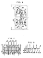
- Fig. 5 shows an electrical connection of a further embodiment of a GTO thyristor stack in accordance with the invention.
- a pair of flat type GTO thyristors may be stacked in the middle of the stack structure and sandwiched by diodes in electrically anti-parallel connection.
- FIGs. 6,7 and 8 similar to Figs. 2, and 4, show a still further embodiment of a GTO thyristor stack in accordance with the invention, in which the same elements as those in Figs. 2, 3 and 4 are designated by the same reference numerals and will not be detailed.
Landscapes
- Engineering & Computer Science (AREA)
- Power Engineering (AREA)
- Microelectronics & Electronic Packaging (AREA)
- Computer Hardware Design (AREA)
- General Physics & Mathematics (AREA)
- Condensed Matter Physics & Semiconductors (AREA)
- Physics & Mathematics (AREA)
- Ceramic Engineering (AREA)
- Inverter Devices (AREA)
- Power Conversion In General (AREA)
- Rectifiers (AREA)
- Metal-Oxide And Bipolar Metal-Oxide Semiconductor Integrated Circuits (AREA)
- Logic Circuits (AREA)
Claims (7)
Applications Claiming Priority (2)
| Application Number | Priority Date | Filing Date | Title |
|---|---|---|---|
| JP107100/81 | 1981-07-10 | ||
| JP56107100A JPS589349A (ja) | 1981-07-10 | 1981-07-10 | Gtoスタツク |
Publications (3)
| Publication Number | Publication Date |
|---|---|
| EP0069971A1 EP0069971A1 (de) | 1983-01-19 |
| EP0069971B1 true EP0069971B1 (de) | 1985-11-21 |
| EP0069971B2 EP0069971B2 (de) | 1989-06-14 |
Family
ID=14450455
Family Applications (1)
| Application Number | Title | Priority Date | Filing Date |
|---|---|---|---|
| EP82106030A Expired EP0069971B2 (de) | 1981-07-10 | 1982-07-06 | Stapel mit GTO-Thyristoren |
Country Status (6)
| Country | Link |
|---|---|
| US (1) | US4492975A (de) |
| EP (1) | EP0069971B2 (de) |
| JP (1) | JPS589349A (de) |
| KR (1) | KR840000983A (de) |
| BR (1) | BR8204010A (de) |
| DE (1) | DE3267574D1 (de) |
Cited By (1)
| Publication number | Priority date | Publication date | Assignee | Title |
|---|---|---|---|---|
| DE4023687A1 (de) * | 1990-07-26 | 1992-01-30 | Asea Brown Boveri | Stromrichteranordnung |
Families Citing this family (27)
| Publication number | Priority date | Publication date | Assignee | Title |
|---|---|---|---|---|
| EP0100626A3 (de) * | 1982-07-29 | 1985-11-06 | LUCAS INDUSTRIES public limited company | Halbleiterzusammenbau |
| JPS59145559A (ja) * | 1983-02-09 | 1984-08-21 | Hitachi Ltd | 半導体スタツク |
| JPS6194362A (ja) * | 1984-10-15 | 1986-05-13 | Mitsubishi Electric Corp | サイリスタ装置 |
| DE3586735D1 (de) * | 1984-10-19 | 1992-11-12 | Bbc Brown Boveri & Cie | Abschaltbares leistungshalbleiterbauelement. |
| EP0185181B1 (de) * | 1984-11-28 | 1990-05-16 | BBC Brown Boveri AG | Induktionsarme Anoden-Kathodenbeschaltung eines abschaltbaren Leistungsthyristors |
| CH668667A5 (de) * | 1985-11-15 | 1989-01-13 | Bbc Brown Boveri & Cie | Leistungshalbleitermodul. |
| US4868712A (en) * | 1987-02-04 | 1989-09-19 | Woodman John K | Three dimensional integrated circuit package |
| JPS6488076A (en) * | 1987-06-12 | 1989-04-03 | Hitachi Ltd | Cryostat |
| US4864385A (en) * | 1987-12-29 | 1989-09-05 | Hitachi, Ltd. | Power semiconductors connected antiparallel via heatsinks |
| US4899088A (en) * | 1988-08-31 | 1990-02-06 | Honeywell Inc. | Power control circuit for inductive loads |
| US4937504A (en) * | 1988-08-31 | 1990-06-26 | Honeywell Inc. | Time delay initialization circuit |
| US4947079A (en) * | 1988-08-31 | 1990-08-07 | Honeywell Inc. | Notch cutting circuit with minimal power dissipation |
| EP0380799B1 (de) * | 1989-02-02 | 1993-10-06 | Asea Brown Boveri Ag | Druckkontaktiertes Halbleiterbauelement |
| WO1991009460A1 (en) * | 1989-12-20 | 1991-06-27 | Sundstrand Corporation | Low inductance converter phase assembly |
| US5043797A (en) * | 1990-04-03 | 1991-08-27 | General Electric Company | Cooling header connection for a thyristor stack |
| FR2747857B1 (fr) * | 1996-04-18 | 1998-05-22 | Gec Alsthom Transport Sa | Dispositif a empilement de thyristors et de diodes de roue libre |
| US5798916A (en) * | 1997-03-20 | 1998-08-25 | Electric Power Research Institute, Inc. | High power inverter pole employing series connected devices configured for reduced stray loop inductance |
| US6333664B1 (en) * | 2000-08-22 | 2001-12-25 | Agere Systems Guardian Corp. | Low operating power, high voltage ringing switch circuit |
| CA2425111C (en) | 2000-11-03 | 2010-06-01 | Smc Electrical Products, Inc. | Microdrive |
| US6713898B2 (en) * | 2001-12-05 | 2004-03-30 | General Electric Company | Internal reactor thyristor stack |
| DE10303463B4 (de) * | 2003-01-29 | 2006-06-14 | Infineon Technologies Ag | Halbleiterbauelement mit wenigstens zwei in einem Gehäuse integrierten und durch einen gemeinsamen Kontaktbügel kontaktierten Chips |
| DE102007039916A1 (de) * | 2007-08-23 | 2009-02-26 | Siemens Ag | Aufbau- und Verbindungstechnik von Modulen mittels dreidimensional geformter Leadframes |
| FR2947949B1 (fr) * | 2009-07-08 | 2012-03-02 | Centre Nat Rech Scient | Module electronique de puissance |
| DE202013104510U1 (de) * | 2013-10-04 | 2013-11-14 | Abb Technology Ag | Halbleiterstapel für Umrichter mit Snubber-Kondensatoren |
| DE202014104564U1 (de) * | 2014-09-24 | 2014-11-20 | Sma Solar Technology Ag | Kurzschlussschalter mit Halbleiterschalter und Anordnung zum Kurzschließen einer dreiphasigen Wechselspannung |
| US10230260B2 (en) | 2015-09-23 | 2019-03-12 | Abb Schweiz Ag | Fast utility disconnect switch for single conversion UPS |
| CN105489572B (zh) * | 2015-12-04 | 2018-01-23 | 许继集团有限公司 | 功率元件模块及其散热器 |
Family Cites Families (11)
| Publication number | Priority date | Publication date | Assignee | Title |
|---|---|---|---|---|
| US3447118A (en) * | 1966-08-16 | 1969-05-27 | Westinghouse Electric Corp | Stacking module for flat packaged electrical devices |
| GB1191887A (en) * | 1966-09-02 | 1970-05-13 | Gen Electric | Semiconductor Rectifier Assemblies |
| AT271630B (de) * | 1966-10-11 | 1969-06-10 | Asea Ab | Stromrichterventil mit Thyristoren |
| FR1587785A (de) * | 1968-10-02 | 1970-03-27 | ||
| US3573574A (en) * | 1969-08-12 | 1971-04-06 | Gen Motors Corp | Controlled rectifier mounting assembly |
| US3753052A (en) * | 1972-03-01 | 1973-08-14 | Gen Electric | Rectifier bridge assembly comprising stack of high-current pn semiconductor wafers in a sealed housing whose end caps comprise ac terminals of the bridge |
| GB1384175A (en) * | 1972-06-01 | 1975-02-19 | Berkovich E I | Electrical frequency changers |
| DE2348207A1 (de) * | 1973-09-25 | 1975-04-17 | Siemens Ag | Thyristorsaeule |
| US4177479A (en) * | 1975-09-09 | 1979-12-04 | Bbc Brown Boveri & Company | Electrical circuit with a high-frequency thyristor fired by blocking leakage current |
| DE2838412A1 (de) * | 1978-09-02 | 1980-06-19 | Bosch Gmbh Robert | Gleichrichteranordnung |
| US4203040A (en) * | 1978-06-30 | 1980-05-13 | Westinghouse Electric Corp. | Force commutated static isolator circuit |
-
1981
- 1981-07-10 JP JP56107100A patent/JPS589349A/ja active Pending
-
1982
- 1982-06-21 KR KR1019820002752A patent/KR840000983A/ko unknown
- 1982-07-06 EP EP82106030A patent/EP0069971B2/de not_active Expired
- 1982-07-06 DE DE8282106030T patent/DE3267574D1/de not_active Expired
- 1982-07-08 US US06/396,377 patent/US4492975A/en not_active Expired - Fee Related
- 1982-07-09 BR BR8204010A patent/BR8204010A/pt unknown
Cited By (2)
| Publication number | Priority date | Publication date | Assignee | Title |
|---|---|---|---|---|
| DE4023687A1 (de) * | 1990-07-26 | 1992-01-30 | Asea Brown Boveri | Stromrichteranordnung |
| DE4023687C2 (de) * | 1990-07-26 | 2000-09-07 | Abb Schweiz Ag | Stromrichteranordnung |
Also Published As
| Publication number | Publication date |
|---|---|
| JPS589349A (ja) | 1983-01-19 |
| BR8204010A (pt) | 1983-07-05 |
| EP0069971B2 (de) | 1989-06-14 |
| EP0069971A1 (de) | 1983-01-19 |
| KR840000983A (ko) | 1984-03-26 |
| DE3267574D1 (en) | 1986-01-02 |
| US4492975A (en) | 1985-01-08 |
Similar Documents
| Publication | Publication Date | Title |
|---|---|---|
| EP0069971B1 (de) | Stapel mit GTO-Thyristoren | |
| US6028779A (en) | Power inverter device | |
| US5031069A (en) | Integration of ceramic capacitor | |
| US5574312A (en) | Low-inductance power semiconductor module | |
| EP1662568B1 (de) | Leistungsmodul, Phasenzweig und Dreiphasenwechselrichter | |
| US5892279A (en) | Packaging for electronic power devices and applications using the packaging | |
| JP3228021B2 (ja) | インバータユニット及びインバータ装置 | |
| JP3229931B2 (ja) | 3レベル電力変換装置 | |
| US11823971B2 (en) | Power electronics system | |
| EP3528605B1 (de) | Kompakte bauweise von mehrstufigen stromrichtersystemen | |
| US5811878A (en) | High-power semiconductor module | |
| US5835362A (en) | Current conductor arrangement | |
| US5617293A (en) | Bridge module | |
| US11817794B2 (en) | Electronic circuit module | |
| JPH04229078A (ja) | 電力変換装置 | |
| US4864385A (en) | Power semiconductors connected antiparallel via heatsinks | |
| JP2002171768A (ja) | 電力変換装置 | |
| US4056767A (en) | Cooling arrangement for semiconductor converter device | |
| JP2001238460A (ja) | 電力変換装置 | |
| US11387219B2 (en) | Power semiconductor module with power semiconductor switches | |
| US20210211061A1 (en) | Converter | |
| JP3646044B2 (ja) | 電力変換装置 | |
| JPH09135155A (ja) | 半導体装置 | |
| US5898582A (en) | Device comprising a stack of thyristors and freewheel diodes | |
| CN114097078B (zh) | 具有集成电涌放电器的功率半导体模块 |
Legal Events
| Date | Code | Title | Description |
|---|---|---|---|
| PUAI | Public reference made under article 153(3) epc to a published international application that has entered the european phase |
Free format text: ORIGINAL CODE: 0009012 |
|
| AK | Designated contracting states |
Designated state(s): DE FR |
|
| 17P | Request for examination filed |
Effective date: 19830527 |
|
| GRAA | (expected) grant |
Free format text: ORIGINAL CODE: 0009210 |
|
| AK | Designated contracting states |
Designated state(s): DE FR |
|
| REF | Corresponds to: |
Ref document number: 3267574 Country of ref document: DE Date of ref document: 19860102 |
|
| ET | Fr: translation filed | ||
| PLBI | Opposition filed |
Free format text: ORIGINAL CODE: 0009260 |
|
| 26 | Opposition filed |
Opponent name: BBC AKTIENGESELLSCHAFT BROWN,BOVERI & CIE. Effective date: 19860821 |
|
| PUAH | Patent maintained in amended form |
Free format text: ORIGINAL CODE: 0009272 |
|
| STAA | Information on the status of an ep patent application or granted ep patent |
Free format text: STATUS: PATENT MAINTAINED AS AMENDED |
|
| 27A | Patent maintained in amended form |
Effective date: 19890614 |
|
| AK | Designated contracting states |
Kind code of ref document: B2 Designated state(s): DE FR |
|
| ET3 | Fr: translation filed ** decision concerning opposition | ||
| PGFP | Annual fee paid to national office [announced via postgrant information from national office to epo] |
Ref country code: FR Payment date: 19920615 Year of fee payment: 11 |
|
| PGFP | Annual fee paid to national office [announced via postgrant information from national office to epo] |
Ref country code: DE Payment date: 19920930 Year of fee payment: 11 |
|
| PG25 | Lapsed in a contracting state [announced via postgrant information from national office to epo] |
Ref country code: FR Effective date: 19940331 |
|
| PG25 | Lapsed in a contracting state [announced via postgrant information from national office to epo] |
Ref country code: DE Effective date: 19940401 |
|
| REG | Reference to a national code |
Ref country code: FR Ref legal event code: ST |