EP0068939A1 - Dispositif d'affichage à cristal liquide associant deux modes d'adressage - Google Patents
Dispositif d'affichage à cristal liquide associant deux modes d'adressage Download PDFInfo
- Publication number
- EP0068939A1 EP0068939A1 EP82401014A EP82401014A EP0068939A1 EP 0068939 A1 EP0068939 A1 EP 0068939A1 EP 82401014 A EP82401014 A EP 82401014A EP 82401014 A EP82401014 A EP 82401014A EP 0068939 A1 EP0068939 A1 EP 0068939A1
- Authority
- EP
- European Patent Office
- Prior art keywords
- electrodes
- layer
- liquid crystal
- electrode
- heating
- Prior art date
- Legal status (The legal status is an assumption and is not a legal conclusion. Google has not performed a legal analysis and makes no representation as to the accuracy of the status listed.)
- Withdrawn
Links
- 239000004973 liquid crystal related substance Substances 0.000 title claims abstract description 23
- 238000010438 heat treatment Methods 0.000 claims abstract description 14
- 239000004990 Smectic liquid crystal Substances 0.000 claims abstract description 8
- 230000003287 optical effect Effects 0.000 claims abstract description 8
- 238000001816 cooling Methods 0.000 claims description 3
- 239000011159 matrix material Substances 0.000 abstract description 9
- 230000000694 effects Effects 0.000 description 6
- PEDCQBHIVMGVHV-UHFFFAOYSA-N Glycerine Chemical compound OCC(O)CO PEDCQBHIVMGVHV-UHFFFAOYSA-N 0.000 description 4
- 210000004027 cell Anatomy 0.000 description 4
- 239000000463 material Substances 0.000 description 4
- 238000009792 diffusion process Methods 0.000 description 3
- 230000005684 electric field Effects 0.000 description 3
- 230000005855 radiation Effects 0.000 description 3
- 229910052782 aluminium Inorganic materials 0.000 description 2
- XAGFODPZIPBFFR-UHFFFAOYSA-N aluminium Chemical compound [Al] XAGFODPZIPBFFR-UHFFFAOYSA-N 0.000 description 2
- 230000006870 function Effects 0.000 description 2
- 238000000034 method Methods 0.000 description 2
- JLSAWPFOOOYLMU-UHFFFAOYSA-N 9-(2-phenylphenyl)nonanenitrile Chemical group N#CCCCCCCCCC1=CC=CC=C1C1=CC=CC=C1 JLSAWPFOOOYLMU-UHFFFAOYSA-N 0.000 description 1
- JBRZTFJDHDCESZ-UHFFFAOYSA-N AsGa Chemical compound [As]#[Ga] JBRZTFJDHDCESZ-UHFFFAOYSA-N 0.000 description 1
- 229910001218 Gallium arsenide Inorganic materials 0.000 description 1
- ATJFFYVFTNAWJD-UHFFFAOYSA-N Tin Chemical compound [Sn] ATJFFYVFTNAWJD-UHFFFAOYSA-N 0.000 description 1
- 238000010276 construction Methods 0.000 description 1
- 239000013078 crystal Substances 0.000 description 1
- 210000002858 crystal cell Anatomy 0.000 description 1
- 238000012217 deletion Methods 0.000 description 1
- 230000037430 deletion Effects 0.000 description 1
- 239000011521 glass Substances 0.000 description 1
- 229910003437 indium oxide Inorganic materials 0.000 description 1
- PJXISJQVUVHSOJ-UHFFFAOYSA-N indium(iii) oxide Chemical compound [O-2].[O-2].[O-2].[In+3].[In+3] PJXISJQVUVHSOJ-UHFFFAOYSA-N 0.000 description 1
- 230000010354 integration Effects 0.000 description 1
- 238000004519 manufacturing process Methods 0.000 description 1
- 229910052751 metal Inorganic materials 0.000 description 1
- 239000002184 metal Substances 0.000 description 1
- 239000000203 mixture Substances 0.000 description 1
- 239000002245 particle Substances 0.000 description 1
- 238000001454 recorded image Methods 0.000 description 1
- 239000004065 semiconductor Substances 0.000 description 1
- 239000007787 solid Substances 0.000 description 1
- 239000000758 substrate Substances 0.000 description 1
- 229910001887 tin oxide Inorganic materials 0.000 description 1
- 230000007704 transition Effects 0.000 description 1
- 239000012780 transparent material Substances 0.000 description 1
Images
Classifications
-
- G—PHYSICS
- G02—OPTICS
- G02F—OPTICAL DEVICES OR ARRANGEMENTS FOR THE CONTROL OF LIGHT BY MODIFICATION OF THE OPTICAL PROPERTIES OF THE MEDIA OF THE ELEMENTS INVOLVED THEREIN; NON-LINEAR OPTICS; FREQUENCY-CHANGING OF LIGHT; OPTICAL LOGIC ELEMENTS; OPTICAL ANALOGUE/DIGITAL CONVERTERS
- G02F1/00—Devices or arrangements for the control of the intensity, colour, phase, polarisation or direction of light arriving from an independent light source, e.g. switching, gating or modulating; Non-linear optics
- G02F1/01—Devices or arrangements for the control of the intensity, colour, phase, polarisation or direction of light arriving from an independent light source, e.g. switching, gating or modulating; Non-linear optics for the control of the intensity, phase, polarisation or colour
- G02F1/13—Devices or arrangements for the control of the intensity, colour, phase, polarisation or direction of light arriving from an independent light source, e.g. switching, gating or modulating; Non-linear optics for the control of the intensity, phase, polarisation or colour based on liquid crystals, e.g. single liquid crystal display cells
- G02F1/132—Thermal activation of liquid crystals exhibiting a thermo-optic effect
-
- G—PHYSICS
- G09—EDUCATION; CRYPTOGRAPHY; DISPLAY; ADVERTISING; SEALS
- G09G—ARRANGEMENTS OR CIRCUITS FOR CONTROL OF INDICATING DEVICES USING STATIC MEANS TO PRESENT VARIABLE INFORMATION
- G09G3/00—Control arrangements or circuits, of interest only in connection with visual indicators other than cathode-ray tubes
- G09G3/02—Control arrangements or circuits, of interest only in connection with visual indicators other than cathode-ray tubes by tracing or scanning a light beam on a screen
-
- G—PHYSICS
- G09—EDUCATION; CRYPTOGRAPHY; DISPLAY; ADVERTISING; SEALS
- G09G—ARRANGEMENTS OR CIRCUITS FOR CONTROL OF INDICATING DEVICES USING STATIC MEANS TO PRESENT VARIABLE INFORMATION
- G09G3/00—Control arrangements or circuits, of interest only in connection with visual indicators other than cathode-ray tubes
- G09G3/20—Control arrangements or circuits, of interest only in connection with visual indicators other than cathode-ray tubes for presentation of an assembly of a number of characters, e.g. a page, by composing the assembly by combination of individual elements arranged in a matrix no fixed position being assigned to or needed to be assigned to the individual characters or partial characters
- G09G3/34—Control arrangements or circuits, of interest only in connection with visual indicators other than cathode-ray tubes for presentation of an assembly of a number of characters, e.g. a page, by composing the assembly by combination of individual elements arranged in a matrix no fixed position being assigned to or needed to be assigned to the individual characters or partial characters by control of light from an independent source
- G09G3/36—Control arrangements or circuits, of interest only in connection with visual indicators other than cathode-ray tubes for presentation of an assembly of a number of characters, e.g. a page, by composing the assembly by combination of individual elements arranged in a matrix no fixed position being assigned to or needed to be assigned to the individual characters or partial characters by control of light from an independent source using liquid crystals
- G09G3/3603—Control arrangements or circuits, of interest only in connection with visual indicators other than cathode-ray tubes for presentation of an assembly of a number of characters, e.g. a page, by composing the assembly by combination of individual elements arranged in a matrix no fixed position being assigned to or needed to be assigned to the individual characters or partial characters by control of light from an independent source using liquid crystals with thermally addressed liquid crystals
Definitions
- the present invention relates to liquid crystal cells, and more particularly those using a liquid crystal in the smectic phase for the purpose of displaying images or patterns. It relates more particularly to devices implementing two addressing modes: optical addressing by laser beam and matrix addressing by heating electrodes.
- thermo-optical effect in liquid crystals of smectic phase for the storage and display of information.
- This effect has in particular been used in an optical valve with laser addressing for the production of a high resolution projection display.
- a screen with 2000 x 2000 resolution points is easily achievable.
- the typical point size is then 20 microns.
- To erase the recorded image it is possible either to scan the cell with the light beam at full intensity and then cool the layer slowly, or to subject the layer to an alternating field with or without beam scanning.
- the problem with this type of display is, however, for some applications, its writing speed: of the order of some 10 4 points per second.
- the present invention proposes to combine these two types of display in order to respond to the often posed problem of a high resolution display and slow to moderate renewal rate (a few seconds for example) which can also allow the display of information at a rapid rate.
- This will generally be the display of a few alphanumeric characters in one of the corners of the screen (scrolling of a counter, a index, time, etc.).
- the proposed device is in particular intended to be observed in reflection and projection on a screen.
- the mesomorphic material can also contain dispersed particles having a modulating effect on the reading radiation of the cell.
- the subject of the invention is a data display device comprising a layer of mesomorphic material having a smectic phase and means making it possible to modify the optical properties of said layer under the influence of electrical signals representative of said data; said layer being disposed between electrodes; characterized in that one of said electrodes has a first continuous area and a second area formed by parallel heating strips; the other electrodes comprising opposite said first area a continuous electrode and facing said second area an array of conductive strips crossing said heating strips; the assembly formed by said liquid crystal layer and said electrodes being sandwiched between two plates, at least one of which is transparent.
- the liquid crystal used has a smectic phase A, that is to say that the long molecules which constitute the mesomorphic material are perpendicular to the plane of the layers. This alignment was facilitated by adequate treatment of the walls. The crystal is therefore transparent in the rest state.
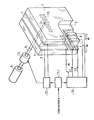
- the liquid crystal layer 1 is sandwiched between two supports 3 and 7 provided with electrodes.
- a first aluminum electrode 2 deposited on a glass substrate 3 previously covered with a multilayer treatment not shown, comprises a continuous range reserved for the laser addressing mode and in a cutout of this range a set of teeth 4 assigned to the mode matrix addressing.
- the support 7 carries a second electrode composed of a continuous range 5 having the same morphology as the continuous range of the electrode 2.
- Track 5 is arranged opposite the other continuous track as shown in the figure.
- the support 7 also carries a network of conductive strips 6 arranged in a cutout of the electrode 5; these conductive strips 6 forming with the electrode 5 a set of insulated electrodes.
- the network 6 of coplanar bands is oriented in such a way that it covers the network of teeth 4, each tooth facing all the bands of the network 6. This arrangement which can be orthogonal forms a set of crossings allowing electrical addressing to be carried out.
- the electrodes carried by at least one of the supports 3 and 7 are formed from a transparent material. For example, they may be deposits of tin or indium oxide or a mixture of these two oxides (ITO electrode).
- the support 7 can be made like the support 3.
- the multilayer treatment mentioned above is intended to adapt the index of the support 3 or 7 to that of the aluminum in order to ensure with the minimum of reflection the transfer of the light radiation to the metal layer during laser addressing.
- We know that the energy transported by this radiation is used to heat the liquid crystal layer. It is then possible to address the layer of liquid crystal in a first sector delimited by the extent of the continuous ranges of the electrodes 2 and 5 by means of a laser beam 8 supplied by a laser 9.
- the laser 9 can be a gallium arsenide semiconductor laser or a laser with a solid active medium of the YAG type.
- a second sector of the liquid crystal layer between the conductive strips 6 and the teeth 4 is subjected to a matrix addressing by heating electrodes.
- the teeth 4 are arranged in a network, for example at a pitch of 20 microns in order to obtain the same resolution as on the part of the screen having a display by laser beam.
- the electrode 2 being grounded, the teeth 4 which in this example are the lines of the matrix network, have one of their ends to ground.
- An electronic device 10 delivers heating voltages for each tooth 4, in order to carry the liquid crystal compared to the temperature allowing to exploit the thermo-optical effect during the cooling following the heating. We know that the thermo-optical effect can be applied in two different ways depending on whether the data to be displayed influences the intensity of the beam 8 or the value of an electric field induced in the liquid crystal layer 1 by the electrodes 2 and 5.
- the appended figure also shows the device controlling the two addressing modes of the cell.
- the data to be displayed is in the form of electrical signals applied to the input of a switching circuit II which distributes them according to their display mode, that is to the input of a deflection control circuit 12, either towards the input of a control circuit 10.
- the circuit 12 controls an optical deflector 13 intended to scan the continuous range by means of the spot 14 produced by the impact of the beam 8.
- the spot 14 can describe a scanning frame represented in the figure by the dotted trace 15.
- the circuit 12 supplies the electrodes 2 and 5 so as to simultaneously induce an electric field in the layer of liquid crystal. This electric field, the intensity of which is a function of the data to be displayed, cooperates with the scanning of the beam to achieve, at each point of the liquid crystal layer, the desired state of diffusion.
- an advantageous method consists in applying an alternating erasing voltage between the electrodes 2 and 5.
Landscapes
- Physics & Mathematics (AREA)
- Engineering & Computer Science (AREA)
- General Physics & Mathematics (AREA)
- Nonlinear Science (AREA)
- Chemical & Material Sciences (AREA)
- Crystallography & Structural Chemistry (AREA)
- Computer Hardware Design (AREA)
- Theoretical Computer Science (AREA)
- Optics & Photonics (AREA)
- Liquid Crystal (AREA)
- Devices For Indicating Variable Information By Combining Individual Elements (AREA)
Applications Claiming Priority (2)
| Application Number | Priority Date | Filing Date | Title |
|---|---|---|---|
| FR8111394 | 1981-06-10 | ||
| FR8111394A FR2507802A1 (fr) | 1981-06-10 | 1981-06-10 | Dispositif d'affichage a cristal liquide associant deux modes d'adressage |
Publications (1)
| Publication Number | Publication Date |
|---|---|
| EP0068939A1 true EP0068939A1 (fr) | 1983-01-05 |
Family
ID=9259346
Family Applications (1)
| Application Number | Title | Priority Date | Filing Date |
|---|---|---|---|
| EP82401014A Withdrawn EP0068939A1 (fr) | 1981-06-10 | 1982-06-04 | Dispositif d'affichage à cristal liquide associant deux modes d'adressage |
Country Status (6)
| Country | Link |
|---|---|
| US (1) | US4499458A (OSRAM) |
| EP (1) | EP0068939A1 (OSRAM) |
| JP (1) | JPS57212416A (OSRAM) |
| KR (1) | KR840000816A (OSRAM) |
| FR (1) | FR2507802A1 (OSRAM) |
| GB (1) | GB2100046B (OSRAM) |
Cited By (3)
| Publication number | Priority date | Publication date | Assignee | Title |
|---|---|---|---|---|
| EP0144683A3 (en) * | 1983-12-12 | 1986-01-08 | International Business Machines Corporation | Alignment layer orientation in liquid crystal displays |
| WO1989003578A1 (en) * | 1987-10-06 | 1989-04-20 | The General Electric Company, Plc | Devices and process for producing microfilm and microfiche records |
| EP0322903A3 (en) * | 1987-12-29 | 1990-11-22 | Canon Kabushiki Kaisha | Optical image recording apparatus |
Families Citing this family (16)
| Publication number | Priority date | Publication date | Assignee | Title |
|---|---|---|---|---|
| JPS5887535A (ja) * | 1981-11-20 | 1983-05-25 | Sony Corp | 液晶表示装置 |
| US4574282A (en) * | 1983-03-18 | 1986-03-04 | International Standard Electric Corporation | Coherent light image generation |
| JPS60175077A (ja) * | 1984-02-22 | 1985-09-09 | 株式会社日立製作所 | 情報保持装置 |
| US4535056A (en) * | 1984-03-15 | 1985-08-13 | Minnesota Mining And Manufacturing Company | Yellow color formers for use in color photothermographic system |
| US4712878A (en) * | 1985-01-18 | 1987-12-15 | Canon Kabushiki Kaisha | Color image forming apparatus comprising ferroelectric smectic liquid crystal having at least two stable states |
| US4751509A (en) * | 1985-06-04 | 1988-06-14 | Nec Corporation | Light valve for use in a color display unit with a diffraction grating assembly included in the valve |
| GB2178581B (en) * | 1985-07-12 | 1989-07-19 | Canon Kk | Liquid crystal apparatus and driving method therefor |
| US4815035A (en) * | 1986-04-08 | 1989-03-21 | Trw Inc. | Scrolling liquid crystal spatial light modulator |
| US4911536A (en) * | 1986-05-08 | 1990-03-27 | Ditzik Richard J | Interactive graphic comunications terminal |
| US4799770A (en) * | 1986-10-02 | 1989-01-24 | Greyhawk Systems, Inc. | Liquid crystal cell for image projections and method of operating same |
| JPH01185692A (ja) * | 1988-01-19 | 1989-07-25 | Sanyo Electric Co Ltd | 平面ディスプレイパネル |
| US5268776A (en) * | 1988-03-18 | 1993-12-07 | Hitachi, Ltd. | System for partially erasing thermally written liquid crystal element |
| US5036317A (en) * | 1988-08-22 | 1991-07-30 | Tektronix, Inc. | Flat panel apparatus for addressing optical data storage locations |
| JP2810070B2 (ja) * | 1988-11-28 | 1998-10-15 | 株式会社リコー | 強誘電性高分子光メモリー |
| US5130703A (en) * | 1989-06-30 | 1992-07-14 | Poqet Computer Corp. | Power system and scan method for liquid crystal display |
| US5589849A (en) * | 1989-07-03 | 1996-12-31 | Ditzik; Richard J. | Display monitor position adjustment apparatus |
Citations (3)
| Publication number | Priority date | Publication date | Assignee | Title |
|---|---|---|---|---|
| FR2275087A1 (fr) * | 1974-06-14 | 1976-01-09 | Thomson Csf | Dispositif de reproduction d'images en noir et blanc utilisant un materiau presentant une phase smectique et systeme de teletransmission et telereprographie mettant en oeuvre ce dispositif |
| FR2389955A1 (OSRAM) * | 1977-05-05 | 1978-12-01 | Thomson Csf | |
| US4270846A (en) * | 1977-12-26 | 1981-06-02 | Kabushiki Kaisha Deini Seikosha | Electro-optical display device |
Family Cites Families (4)
| Publication number | Priority date | Publication date | Assignee | Title |
|---|---|---|---|---|
| FR2296198A1 (fr) * | 1974-12-24 | 1976-07-23 | Commissariat Energie Atomique | Procede thermique de commande de proprietes optiques d'un cristal liquide et dispositifs mettant en oeuvre ledit procede |
| FR2410924A1 (fr) * | 1977-12-01 | 1979-06-29 | Thomson Csf | Procede de telecopie utilisant une cellule a cristal liquide smectique et telecopieur emetteur-recepteur mettant en oeuvre ce procede |
| FR2489564A1 (fr) * | 1980-09-02 | 1982-03-05 | Thomson Csf | Procede et dispositif de visualisation utilisant un effet thermo-optique avec memoire dans une couche mince de cristal liquide disquotique |
| US4391492A (en) * | 1981-04-06 | 1983-07-05 | Minnesota Mining And Manufacturing Company | Thermally addressed cholesteric-smectic liquid crystal device |
-
1981
- 1981-06-10 FR FR8111394A patent/FR2507802A1/fr active Granted
-
1982
- 1982-06-04 EP EP82401014A patent/EP0068939A1/fr not_active Withdrawn
- 1982-06-08 KR KR1019820002558A patent/KR840000816A/ko not_active Withdrawn
- 1982-06-08 GB GB8216568A patent/GB2100046B/en not_active Expired
- 1982-06-09 US US06/386,522 patent/US4499458A/en not_active Expired - Fee Related
- 1982-06-10 JP JP57098572A patent/JPS57212416A/ja active Pending
Patent Citations (3)
| Publication number | Priority date | Publication date | Assignee | Title |
|---|---|---|---|---|
| FR2275087A1 (fr) * | 1974-06-14 | 1976-01-09 | Thomson Csf | Dispositif de reproduction d'images en noir et blanc utilisant un materiau presentant une phase smectique et systeme de teletransmission et telereprographie mettant en oeuvre ce dispositif |
| FR2389955A1 (OSRAM) * | 1977-05-05 | 1978-12-01 | Thomson Csf | |
| US4270846A (en) * | 1977-12-26 | 1981-06-02 | Kabushiki Kaisha Deini Seikosha | Electro-optical display device |
Non-Patent Citations (2)
| Title |
|---|
| APPLIED PHYSICS LETTERS, vol.22, no.3, 1er février 1973, New York (US) * |
| IBM TECHNICAL DISCLOSURE BULLETIN, vol.18, no.11, avril 1976, New York (US) * |
Cited By (4)
| Publication number | Priority date | Publication date | Assignee | Title |
|---|---|---|---|---|
| EP0144683A3 (en) * | 1983-12-12 | 1986-01-08 | International Business Machines Corporation | Alignment layer orientation in liquid crystal displays |
| WO1989003578A1 (en) * | 1987-10-06 | 1989-04-20 | The General Electric Company, Plc | Devices and process for producing microfilm and microfiche records |
| US5157528A (en) * | 1987-10-06 | 1992-10-20 | The General Electric Company, P.L.C. | Devices and process for producing microfilm and microfiche records |
| EP0322903A3 (en) * | 1987-12-29 | 1990-11-22 | Canon Kabushiki Kaisha | Optical image recording apparatus |
Also Published As
| Publication number | Publication date |
|---|---|
| US4499458A (en) | 1985-02-12 |
| GB2100046B (en) | 1984-10-10 |
| JPS57212416A (en) | 1982-12-27 |
| GB2100046A (en) | 1982-12-15 |
| FR2507802A1 (fr) | 1982-12-17 |
| KR840000816A (ko) | 1984-02-27 |
| FR2507802B1 (OSRAM) | 1985-03-08 |
Similar Documents
| Publication | Publication Date | Title |
|---|---|---|
| EP0068939A1 (fr) | Dispositif d'affichage à cristal liquide associant deux modes d'adressage | |
| US4040047A (en) | Erasable thermo-optic storage display of a transmitted image | |
| US4196974A (en) | Smectic liquid crystal display cell | |
| EP0012651A1 (fr) | Dispositif d'affichage à cristal liquide | |
| JPS6217726A (ja) | 表示器 | |
| US4288822A (en) | System for the analysis and the recording of monochromic images | |
| FR2557996A1 (fr) | Procede de formation d'image et appareil pour sa mise en oeuvre. | |
| EP0047198B1 (fr) | Procédé de visualisation utilisant un effet thermo-optique avec mémoire dans une couche mince de cristal liquide disquotique, et cristaux liquides disquotiques présentant un tel effet | |
| EP0402944A2 (en) | Light addressed liquid crystal light valve | |
| US5221980A (en) | Method for driving ferroelectric liquid crystal light valve of light writing type | |
| US4733369A (en) | Method for providing separately adjustable voltage dependent optical properties | |
| FR2511798A1 (fr) | Dispositif de visualisation a cristal liquide smectique | |
| EP0217455B1 (fr) | Relais optique dont la cible fonctionne en mode ferroélectrique | |
| EP0240043A1 (fr) | Relais optique opérant en mode d'accumulation de charges | |
| EP0026127B1 (fr) | Dispositif de visualisation à mémoire | |
| US5040879A (en) | Variable density optical filter | |
| JP2796596B2 (ja) | 空間光変調器の駆動方法及び空間光変調器 | |
| Maydan | Infrared laser addressing of media for recording and displaying of high-resolution graphic information | |
| FR2653247A1 (fr) | Procede et dispositif d'ecriture et de lecture d'informations a partir d'un support a base de materiau ferroelectrique. | |
| CH634690A5 (fr) | Dispositif a couche mince transparente photoconductrice, utilisation de ce dispositif pour constituer une memoire, et procede de fabrication de ce dispositif. | |
| JP3151464B2 (ja) | 光記録媒体および記録方法 | |
| FR2561423A1 (fr) | Dispositif de visualisation a commande electrique | |
| JPH0548883B2 (OSRAM) | ||
| JP2002312936A (ja) | 光記録媒体の記録方法および情報が記録された光記録媒体 | |
| JP3289641B2 (ja) | 映像表示装置およびその駆動方法 |
Legal Events
| Date | Code | Title | Description |
|---|---|---|---|
| PUAI | Public reference made under article 153(3) epc to a published international application that has entered the european phase |
Free format text: ORIGINAL CODE: 0009012 |
|
| AK | Designated contracting states |
Designated state(s): DE IT NL SE |
|
| 17P | Request for examination filed |
Effective date: 19830121 |
|
| STAA | Information on the status of an ep patent application or granted ep patent |
Free format text: STATUS: THE APPLICATION HAS BEEN WITHDRAWN |
|
| 18W | Application withdrawn |
Withdrawal date: 19850711 |
|
| RIN1 | Information on inventor provided before grant (corrected) |
Inventor name: HARENG, MICHEL Inventor name: LE BERRE, SERGE |