EP0068652A2 - Photo diodes - Google Patents
Photo diodes Download PDFInfo
- Publication number
- EP0068652A2 EP0068652A2 EP82302843A EP82302843A EP0068652A2 EP 0068652 A2 EP0068652 A2 EP 0068652A2 EP 82302843 A EP82302843 A EP 82302843A EP 82302843 A EP82302843 A EP 82302843A EP 0068652 A2 EP0068652 A2 EP 0068652A2
- Authority
- EP
- European Patent Office
- Prior art keywords
- cdte
- type
- photo diode
- layer
- substrate
- Prior art date
- Legal status (The legal status is an assumption and is not a legal conclusion. Google has not performed a legal analysis and makes no representation as to the accuracy of the status listed.)
- Granted
Links
- 229910004613 CdTe Inorganic materials 0.000 claims abstract description 59
- 239000000758 substrate Substances 0.000 claims abstract description 22
- 239000002019 doping agent Substances 0.000 claims abstract description 9
- 238000009792 diffusion process Methods 0.000 claims abstract description 6
- 238000010438 heat treatment Methods 0.000 claims abstract description 5
- 239000000463 material Substances 0.000 claims description 12
- 229910052793 cadmium Inorganic materials 0.000 claims description 3
- 125000005842 heteroatom Chemical group 0.000 claims 1
- 238000000034 method Methods 0.000 abstract description 8
- 239000000203 mixture Substances 0.000 description 4
- 230000005855 radiation Effects 0.000 description 2
- 229910000661 Mercury cadmium telluride Inorganic materials 0.000 description 1
- 125000000217 alkyl group Chemical group 0.000 description 1
- 239000000956 alloy Substances 0.000 description 1
- 229910045601 alloy Inorganic materials 0.000 description 1
- 229910052785 arsenic Inorganic materials 0.000 description 1
- 239000013078 crystal Substances 0.000 description 1
- 230000001419 dependent effect Effects 0.000 description 1
- 230000005670 electromagnetic radiation Effects 0.000 description 1
- 230000008020 evaporation Effects 0.000 description 1
- 238000001704 evaporation Methods 0.000 description 1
- 238000002513 implantation Methods 0.000 description 1
- 238000005468 ion implantation Methods 0.000 description 1
- 150000002500 ions Chemical class 0.000 description 1
- 239000007788 liquid Substances 0.000 description 1
- 238000002161 passivation Methods 0.000 description 1
- 229910052698 phosphorus Inorganic materials 0.000 description 1
- 229920002120 photoresistant polymer Polymers 0.000 description 1
- 230000001681 protective effect Effects 0.000 description 1
- 239000004065 semiconductor Substances 0.000 description 1
- 229910052709 silver Inorganic materials 0.000 description 1
- 238000001931 thermography Methods 0.000 description 1
Images
Classifications
-
- H—ELECTRICITY
- H01—ELECTRIC ELEMENTS
- H01L—SEMICONDUCTOR DEVICES NOT COVERED BY CLASS H10
- H01L27/00—Devices consisting of a plurality of semiconductor or other solid-state components formed in or on a common substrate
- H01L27/14—Devices consisting of a plurality of semiconductor or other solid-state components formed in or on a common substrate including semiconductor components sensitive to infrared radiation, light, electromagnetic radiation of shorter wavelength or corpuscular radiation and specially adapted either for the conversion of the energy of such radiation into electrical energy or for the control of electrical energy by such radiation
- H01L27/144—Devices controlled by radiation
- H01L27/146—Imager structures
- H01L27/14643—Photodiode arrays; MOS imagers
- H01L27/14649—Infrared imagers
-
- H—ELECTRICITY
- H01—ELECTRIC ELEMENTS
- H01L—SEMICONDUCTOR DEVICES NOT COVERED BY CLASS H10
- H01L27/00—Devices consisting of a plurality of semiconductor or other solid-state components formed in or on a common substrate
- H01L27/14—Devices consisting of a plurality of semiconductor or other solid-state components formed in or on a common substrate including semiconductor components sensitive to infrared radiation, light, electromagnetic radiation of shorter wavelength or corpuscular radiation and specially adapted either for the conversion of the energy of such radiation into electrical energy or for the control of electrical energy by such radiation
- H01L27/144—Devices controlled by radiation
- H01L27/146—Imager structures
- H01L27/14683—Processes or apparatus peculiar to the manufacture or treatment of these devices or parts thereof
- H01L27/14692—Thin film technologies, e.g. amorphous, poly, micro- or nanocrystalline silicon
Definitions
- This invention relates to photo diodes.
- a photo diode is a two terminal semiconductor device having one terminal attached to a piece of p-type material and the other terminal connected to a piece of n-type material with a p-n junction between the two types of materials. An electron flow occurs across the p-n junction when illuminated by electro magnetic radiation of a suitable wavelength.
- One known photo diode comprises a substrate of p-type Cd x Hg 1-x Te (C.M.T.) on which a layer of ZnS has been grown. This is described e.g. in App. Phy. Letts. 34(1) 1 Jan. 1979, pages 50-52, M Lanir et al. A p-n junction is formed in the bulk of the CdHgTe by ion implantation through the ZnS. Such a device is sensitive to infra red radiation and is therefore useful in thermal imaging systems where the thermal image of a scene is measured and used to form a visible display on a cathode ray tube.
- C.M.T. p-type Cd x Hg 1-x Te
- an infra red sensitive photo diode comprises a piece of Cd x Hg 1-x Te and a piece of CdTe forming a p-n junction with terminals connected to the p and n type materials.
- the Cd x Hg 1-x Te may be p-type in which case the CdTe is n-type or vice versa.
- the n-type CdTe may be grown as a semi-insulating layer with a layer of a group IIIa or VII donor dopant deposited on top and diffused into the CdTe to form n-type CdTe.
- the dopant may be In.
- a p-type CdTe layer may be grown in a similar manner using as dopants P, As, Ag, or Au.
- the CdTe may be grown n-type by molecular beam epitaxial techniques with an In dopant.
- areas of C.M.T. not forming diode junctions may be passivated by a layer of semi-insulating CdTe.
- the CdTe layers may be grown by an suitable epitaxial growth technique, e.g. M.B.E., vapour-growth, etc.
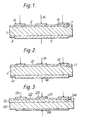
- the substrate 1 is cut, cleaned, and polished and placed in a molecular beam epitaxial (M.B.E.) growth chamber where a protective passivating layer 2, 3 of CdTe is grown on all surfaces.
- Typical layer 2 thickness on top of the substrate 1 is 0.5 ⁇ m in a range of about 0.2 to 1 ⁇ m. Islands 4 of In are deposited, e.g. by evaporation, on the top surface of CdTe 2.
- the structure is then heated typically at 70-120°C for 4 to 40 hours to diffuse In into the CdTe 2 giving n-type heavily doped regions 8 (e.g. number of electrons, n > 5 ⁇ 10 16 cm -3 ) under the islands 4. Additionally this heating causes inter diffusion at the C.M.T. and CdTe interface (p-n junction 7) with Hg diffusing into the CdTe layer 2 and Cd diffusing into the C.M.T. This gives a gradual material composition change creating a graded heterostructure where the p-n junction is close to the heterojunction.
- a back electrode 5, e.g. of Au, is formed through apertures in the bottom CdTe layer direct onto the substrate.
- a top terminal connection 6 is made separately to each In island 4.
- the C.M.T. substrate can be thick in which case no passivation of the bottom surface is necessary although it may be applied as above.
- Infra red radiation incident on the p-n junction 7 causes a measurable voltage or current flow (dependent on the external circuitry) to be developed at the terminals 5, 6.
- Figure 2 shows an alternative form of photo diode array comprising a p-type Cd x Hg 1-x Te substrate 11 with islands 12 of n-type doped'CdTe. Between the islands 12 is a layer 13 of semi-insulating CdTe. A passivating layer 14 of CdTe covers the remaining substrate surfaces.
- the n-type CdTe material 12 is grown in a molecular beam epitaxial chamber using an In dopant source in addition to the Cd, and Te sources. Alternatively the stoichiometry of the CdTe layer may be adjusted to give semi-insulating or semi-conducting layers. Photolithographic techniques are used to define the different parts of the top layer. For example islands of photo resist may be formed on the top surface of the substrate. A semi-insulating layer of CdTe is grown over the islands and top of the substrate. The resist is then lifted off leaving apertures through which n-type CdTe is grown.
- Terminal connections 15, 16 are made to each island and the bottom of the substrate 11 as before.
- the structure is heated e.g. at 70-120 C for 4-40 hours to allow diffusion at the p-n junction 17 as before.
- the composition of the n-type CdTe may be changed during molecular beam epitaxial growth.
- the alloy Cd x Hg 1-x Te may be grown initially and the Hg source gradually reduced until only doped CdTe is being grown.
- Such a graded composition may also be used in the device of Figure 1.
- Figure 3 shows another form of photo diode array. It comprises a p-type semi-conducting substrate 20 of CdTe on which a p-type layer 21 of Cd x Hg 1-x Te is grown (or polished, lapped) to a typical thickness of 10 to 30 ym.
- a semi-insulating layer of CdTe 22 is grown on the layer and islands 23 of In deposited on the CdTe 22 as in Figure 1. As before the device is heated to diffuse the In 23 into the CdTe layer 27, and also cause a diffusion at the p-n junction 24. Terminals 25, 26 are connected top and bottom as before.
- the CdTe 20 may be grown on a supporting base of other suitable material by M.B.E.
- an electrode 26 on the rear surface electrodes may be arranged on the top surface of the C.M.T. 21 to one side of the islands 23.
- the C.M.T. 21 may be grown by liquid, vapour, or molecular beam epitaxial techniques or using alkyls of Cd and Te flowing over the CdTe substrate 20 in an atmosphere of Hg. Such a technique is described in U.K. Patent Application No. 2,078,695 A, U.S.A. Patent Application Serial No. 266,046.
- the n-type CdTe of Figure 3 may alternatively be formed as in Figure 2 using In doped and molecular beam epitaxial techniques.
- the CdTe layer may be selectively n-type doped by implantation of In ions.
- the CdTe layer may be formed with a graded composition i.e. starting by growing C.M.T. and gradually reducing the Hg source.
Abstract
Description
- This invention relates to photo diodes.
- A photo diode is a two terminal semiconductor device having one terminal attached to a piece of p-type material and the other terminal connected to a piece of n-type material with a p-n junction between the two types of materials. An electron flow occurs across the p-n junction when illuminated by electro magnetic radiation of a suitable wavelength.
- One known photo diode comprises a substrate of p-type CdxHg1-xTe (C.M.T.) on which a layer of ZnS has been grown. This is described e.g. in App. Phy. Letts. 34(1) 1 Jan. 1979, pages 50-52, M Lanir et al. A p-n junction is formed in the bulk of the CdHgTe by ion implantation through the ZnS. Such a device is sensitive to infra red radiation and is therefore useful in thermal imaging systems where the thermal image of a scene is measured and used to form a visible display on a cathode ray tube.
- According to this invention an infra red sensitive photo diode comprises a piece of CdxHg1-xTe and a piece of CdTe forming a p-n junction with terminals connected to the p and n type materials. The CdxHg1-xTe may be p-type in which case the CdTe is n-type or vice versa.
- The n-type CdTe may be grown as a semi-insulating layer with a layer of a group IIIa or VII donor dopant deposited on top and diffused into the CdTe to form n-type CdTe. The dopant may be In. A p-type CdTe layer may be grown in a similar manner using as dopants P, As, Ag, or Au.
- Alternatively the CdTe may be grown n-type by molecular beam epitaxial techniques with an In dopant.
- When built as an array of photo diodes, areas of C.M.T. not forming diode junctions may be passivated by a layer of semi-insulating CdTe.
- The CdTe layers may be grown by an suitable epitaxial growth technique, e.g. M.B.E., vapour-growth, etc.
- Growth of layers using M.B.E. techniques is described in Capter 1.7 of Crystal Growth & Materials edited by E. Kaldis & H. J. Scheel published by North Holland Publishing Co., Amsterdam, 1977.
- The invention will now be described, by way of example only, with reference to the accompanying drawings of which:-
- Figure 1 is a cross section of a photo diode array formed on a C.M.T. substrate;
- Figure 2 is an alternative to Figure 1;
- Figure 3 is a photo diode grown on a CdTe substrate.
- The photo diode of Figure 1 comprises a p-type Cd xHg1-xTe (C.M.T.) substrate 1 of thickness 10-30 µm. Typically x is 0.2 to 0.3 16 and acceptor concentration NA = 1 to 5 x 1016cm-3. The substrate 1 is cut, cleaned, and polished and placed in a molecular beam epitaxial (M.B.E.) growth chamber where a protective passivating
layer Typical layer 2 thickness on top of the substrate 1 is 0.5 µm in a range of about 0.2 to 1 µm. Islands 4 of In are deposited, e.g. by evaporation, on the top surface ofCdTe 2. The structure is then heated typically at 70-120°C for 4 to 40 hours to diffuse In into theCdTe 2 giving n-type heavily doped regions 8 (e.g. number of electrons, n > 5 × 1016cm-3) under the islands 4. Additionally this heating causes inter diffusion at the C.M.T. and CdTe interface (p-n junction 7) with Hg diffusing into theCdTe layer 2 and Cd diffusing into the C.M.T. This gives a gradual material composition change creating a graded heterostructure where the p-n junction is close to the heterojunction. Aback electrode 5, e.g. of Au, is formed through apertures in the bottom CdTe layer direct onto the substrate. A top terminal connection 6 is made separately to each In island 4. - As an alternative, the C.M.T. substrate can be thick in which case no passivation of the bottom surface is necessary although it may be applied as above.
- Infra red radiation incident on the
p-n junction 7 causes a measurable voltage or current flow (dependent on the external circuitry) to be developed at theterminals 5, 6. - Figure 2 shows an alternative form of photo diode array comprising a p-type CdxHg1-xTe substrate 11 with islands 12 of n-type doped'CdTe. Between the islands 12 is a
layer 13 of semi-insulating CdTe. Apassivating layer 14 of CdTe covers the remaining substrate surfaces. The n-type CdTe material 12 is grown in a molecular beam epitaxial chamber using an In dopant source in addition to the Cd, and Te sources. Alternatively the stoichiometry of the CdTe layer may be adjusted to give semi-insulating or semi-conducting layers. Photolithographic techniques are used to define the different parts of the top layer. For example islands of photo resist may be formed on the top surface of the substrate. A semi-insulating layer of CdTe is grown over the islands and top of the substrate. The resist is then lifted off leaving apertures through which n-type CdTe is grown. -
Terminal connections - The structure is heated e.g. at 70-120 C for 4-40 hours to allow diffusion at the
p-n junction 17 as before. - Alternatively the composition of the n-type CdTe may be changed during molecular beam epitaxial growth. For example the alloy CdxHg1-xTe may be grown initially and the Hg source gradually reduced until only doped CdTe is being grown. Such a graded composition may also be used in the device of Figure 1.
- Figure 3 shows another form of photo diode array. It comprises a p-type
semi-conducting substrate 20 of CdTe on which a p-type layer 21 of CdxHg1-xTe is grown (or polished, lapped) to a typical thickness of 10 to 30 ym. A semi-insulating layer ofCdTe 22 is grown on the layer andislands 23 of In deposited on theCdTe 22 as in Figure 1. As before the device is heated to diffuse the In 23 into theCdTe layer 27, and also cause a diffusion at thep-n junction 24.Terminals 25, 26 are connected top and bottom as before. - Alternatively the CdTe 20 may be grown on a supporting base of other suitable material by M.B.E. As an alternative to an
electrode 26 on the rear surface electrodes may be arranged on the top surface of the C.M.T. 21 to one side of theislands 23. - The C.M.T. 21 may be grown by liquid, vapour, or molecular beam epitaxial techniques or using alkyls of Cd and Te flowing over the
CdTe substrate 20 in an atmosphere of Hg. Such a technique is described in U.K. Patent Application No. 2,078,695 A, U.S.A. Patent Application Serial No. 266,046. - The n-type CdTe of Figure 3 may alternatively be formed as in Figure 2 using In doped and molecular beam epitaxial techniques. In another form the CdTe layer may be selectively n-type doped by implantation of In ions.
- Also the CdTe layer may be formed with a graded composition i.e. starting by growing C.M.T. and gradually reducing the Hg source.
Claims (14)
Applications Claiming Priority (2)
| Application Number | Priority Date | Filing Date | Title |
|---|---|---|---|
| GB8119440 | 1981-06-24 | ||
| GB8119440 | 1981-06-24 |
Publications (3)
| Publication Number | Publication Date |
|---|---|
| EP0068652A2 true EP0068652A2 (en) | 1983-01-05 |
| EP0068652A3 EP0068652A3 (en) | 1985-05-02 |
| EP0068652B1 EP0068652B1 (en) | 1988-05-25 |
Family
ID=10522768
Family Applications (1)
| Application Number | Title | Priority Date | Filing Date |
|---|---|---|---|
| EP82302843A Expired EP0068652B1 (en) | 1981-06-24 | 1982-06-02 | Photo diodes |
Country Status (6)
| Country | Link |
|---|---|
| US (1) | US4494133A (en) |
| EP (1) | EP0068652B1 (en) |
| JP (1) | JPS582078A (en) |
| DE (1) | DE3278553D1 (en) |
| GB (1) | GB2100927B (en) |
| IL (1) | IL66037A (en) |
Cited By (2)
| Publication number | Priority date | Publication date | Assignee | Title |
|---|---|---|---|---|
| EP0135344A1 (en) * | 1983-09-13 | 1985-03-27 | The Secretary of State for Defence in Her Britannic Majesty's Government of the United Kingdom of Great Britain and | Manufacture of cadmium mercury telluride |
| FR2557562A1 (en) * | 1983-12-29 | 1985-07-05 | Menn Roger | Process for the manufacture of nonconductive layers with change in atomic composition |
Families Citing this family (22)
| Publication number | Priority date | Publication date | Assignee | Title |
|---|---|---|---|---|
| DE3278553D1 (en) * | 1981-06-24 | 1988-06-30 | Secr Defence Brit | Photo diodes |
| JPS599977A (en) * | 1982-07-07 | 1984-01-19 | Mitsubishi Electric Corp | Semiconductor device |
| US4720738A (en) * | 1982-09-08 | 1988-01-19 | Texas Instruments Incorporated | Focal plane array structure including a signal processing system |
| US4549195A (en) * | 1983-04-14 | 1985-10-22 | Westinghouse Electric Corp. | Heterojunction semiconductor device |
| GB8417303D0 (en) * | 1984-07-06 | 1984-08-08 | Secr Defence | Infra-red detector |
| US4646120A (en) * | 1985-03-21 | 1987-02-24 | The United States Of America As Represented By The Secretary Of The Army | Photodiode array |
| US4639756A (en) * | 1986-05-05 | 1987-01-27 | Santa Barbara Research Center | Graded gap inversion layer photodiode array |
| US5936268A (en) * | 1988-03-29 | 1999-08-10 | Raytheon Company | Epitaxial passivation of group II-VI infrared photodetectors |
| US4956304A (en) * | 1988-04-07 | 1990-09-11 | Santa Barbara Research Center | Buried junction infrared photodetector process |
| US5880510A (en) * | 1988-05-11 | 1999-03-09 | Raytheon Company | Graded layer passivation of group II-VI infrared photodetectors |
| FR2633101B1 (en) * | 1988-06-16 | 1992-02-07 | Commissariat Energie Atomique | PHOTODIODE AND MATRIX OF PHOTODIODES ON HGCDTE AND METHODS OF MAKING SAME |
| US4914765A (en) * | 1988-09-21 | 1990-04-10 | Smith Shayne H | Pillow and shovel assembly |
| US4927773A (en) * | 1989-06-05 | 1990-05-22 | Santa Barbara Research Center | Method of minimizing implant-related damage to a group II-VI semiconductor material |
| US4961098A (en) * | 1989-07-03 | 1990-10-02 | Santa Barbara Research Center | Heterojunction photodiode array |
| US5049962A (en) * | 1990-03-07 | 1991-09-17 | Santa Barbara Research Center | Control of optical crosstalk between adjacent photodetecting regions |
| JPH05145093A (en) * | 1991-11-20 | 1993-06-11 | Mitsubishi Electric Corp | Mercury diffusion into semiconductor crystal |
| US5296384A (en) * | 1992-07-21 | 1994-03-22 | Santa Barbara Research Center | Bake-stable HgCdTe photodetector and method for fabricating same |
| EP0635892B1 (en) * | 1992-07-21 | 2002-06-26 | Raytheon Company | Bake-stable HgCdTe photodetector and method for fabricating same |
| US5466953A (en) * | 1993-05-28 | 1995-11-14 | Santa Barbara Research Center | Denuded zone field effect photoconductive detector |
| GB2307785B (en) * | 1995-11-29 | 1998-04-29 | Simage Oy | Forming contacts on semiconductor substrates for radiation detectors and imaging devices |
| JPH09153639A (en) * | 1995-11-30 | 1997-06-10 | Nec Corp | Photovoltaic infrared ray receiving device and manufacture of the same |
| RU2611211C1 (en) * | 2015-11-20 | 2017-02-21 | Акционерное общество "НПО "Орион" | Method of passivating surface of cadmium-mercury telluride |
Citations (2)
| Publication number | Priority date | Publication date | Assignee | Title |
|---|---|---|---|---|
| US3622405A (en) * | 1970-06-22 | 1971-11-23 | Honeywell Inc | Method for reducing compositional gradients in{11 {11 {11 {11 {11 {11 {11 {11 {11 {11 |
| GB2078695A (en) * | 1980-05-27 | 1982-01-13 | Secr Defence | Cadmium Mercury Telluride Deposition |
Family Cites Families (4)
| Publication number | Priority date | Publication date | Assignee | Title |
|---|---|---|---|---|
| FR2336804A1 (en) * | 1975-12-23 | 1977-07-22 | Telecommunications Sa | IMPROVEMENTS MADE TO SEMICONDUCTOR DEVICES, ESPECIALLY TO PHOTOVOLTAIC DETECTORS INCLUDING A SUBSTRATE BASED ON A CDXHG1-XTE ALLOY, AND PROCESS FOR MANUFACTURING SUCH A PERFECTED DEVICE |
| US4377904A (en) * | 1978-10-10 | 1983-03-29 | Texas Instruments Incorporated | Method of fabricating a narrow band-gap semiconductor CCD imaging device |
| US4374678A (en) * | 1981-06-01 | 1983-02-22 | Texas Instruments Incorporated | Process for forming HgCoTe alloys selectively by IR illumination |
| DE3278553D1 (en) * | 1981-06-24 | 1988-06-30 | Secr Defence Brit | Photo diodes |
-
1982
- 1982-06-02 DE DE8282302843T patent/DE3278553D1/en not_active Expired
- 1982-06-02 EP EP82302843A patent/EP0068652B1/en not_active Expired
- 1982-06-03 GB GB08216263A patent/GB2100927B/en not_active Expired
- 1982-06-07 US US06/386,082 patent/US4494133A/en not_active Expired - Lifetime
- 1982-06-11 IL IL66037A patent/IL66037A/en not_active IP Right Cessation
- 1982-06-22 JP JP57107503A patent/JPS582078A/en active Granted
Patent Citations (2)
| Publication number | Priority date | Publication date | Assignee | Title |
|---|---|---|---|---|
| US3622405A (en) * | 1970-06-22 | 1971-11-23 | Honeywell Inc | Method for reducing compositional gradients in{11 {11 {11 {11 {11 {11 {11 {11 {11 {11 |
| GB2078695A (en) * | 1980-05-27 | 1982-01-13 | Secr Defence | Cadmium Mercury Telluride Deposition |
Non-Patent Citations (2)
| Title |
|---|
| APPLIED PHYSICS, vol. 22, no. 1, May 1980, pages 57-60, Heidelberg, DE; M. LANIR et al.: "Characterization of limited-diffusion-volume HgCdTe/CdTe photodiodes" * |
| JOURNAL OF APPLIED PHYSICS, vol. 51, no. 4, April 1980, pages 2255-2257, New York, USA; M. CHU et al.: "Liquid phase epitaxial growth of CdTe/Hg1-xCdxTe multilayers(0.3<x>0.5)" * |
Cited By (2)
| Publication number | Priority date | Publication date | Assignee | Title |
|---|---|---|---|---|
| EP0135344A1 (en) * | 1983-09-13 | 1985-03-27 | The Secretary of State for Defence in Her Britannic Majesty's Government of the United Kingdom of Great Britain and | Manufacture of cadmium mercury telluride |
| FR2557562A1 (en) * | 1983-12-29 | 1985-07-05 | Menn Roger | Process for the manufacture of nonconductive layers with change in atomic composition |
Also Published As
| Publication number | Publication date |
|---|---|
| GB2100927B (en) | 1985-07-31 |
| EP0068652A3 (en) | 1985-05-02 |
| JPS582078A (en) | 1983-01-07 |
| DE3278553D1 (en) | 1988-06-30 |
| GB2100927A (en) | 1983-01-06 |
| JPH0366820B2 (en) | 1991-10-18 |
| IL66037A (en) | 1985-11-29 |
| US4494133A (en) | 1985-01-15 |
| EP0068652B1 (en) | 1988-05-25 |
Similar Documents
| Publication | Publication Date | Title |
|---|---|---|
| US4494133A (en) | Infrared sensitive photo diode | |
| EP0518243B1 (en) | Two-color radiation detector array and method of fabricating same | |
| EP0156156A1 (en) | Avalanche photodiodes | |
| CA1132693A (en) | Demultiplexing photodetector | |
| US5401986A (en) | Bake-stable HgCdTe photodetector with II-VI passivation layer | |
| EP0406696B1 (en) | Heterojunction photodiode array | |
| EP0374232A1 (en) | Method of fabricating an infrared photodetector. | |
| EP1017110A1 (en) | Visible-blind UV detectors | |
| Gertner et al. | High‐performance photovoltaic infrared devices in Hg1− x Cd x Te on GaAs | |
| US4875082A (en) | Schottky barrier photodiode structure | |
| D’souza et al. | VSWIR to VLWIR MBE grown HgCdTe material and detectors for remote sensing applications | |
| US5599733A (en) | Method using cadmium-rich CdTe for lowering the metal vacancy concentrations of HgCdTe surfaces | |
| JPS646547B2 (en) | ||
| US5646426A (en) | Contact metal diffusion barrier for semiconductor devices | |
| US5296384A (en) | Bake-stable HgCdTe photodetector and method for fabricating same | |
| US4742017A (en) | Implantation method for forming Schottky barrier photodiodes | |
| US5177580A (en) | Implant guarded mesa having improved detector uniformity | |
| US4075043A (en) | Liquid phase epitaxy method of growing a junction between two semiconductive materials utilizing an interrupted growth technique | |
| Migliorato et al. | CdTe/HgCdTe indium-diffused photodiodes | |
| Arias et al. | HgCdTe dual‐band infrared photodiodes grown by molecular beam epitaxy | |
| US5182217A (en) | Method of fabricating a trapping-mode | |
| KR20090056934A (en) | Photodetector and method for manufacturing photodetector | |
| Riley et al. | HgCdTe hybrid focal-plane arrays | |
| US5079610A (en) | Structure and method of fabricating a trapping-mode | |
| GB2103878A (en) | Semiconductor devices |
Legal Events
| Date | Code | Title | Description |
|---|---|---|---|
| PUAI | Public reference made under article 153(3) epc to a published international application that has entered the european phase |
Free format text: ORIGINAL CODE: 0009012 |
|
| AK | Designated contracting states |
Designated state(s): DE FR NL |
|
| 17P | Request for examination filed |
Effective date: 19830609 |
|
| PUAL | Search report despatched |
Free format text: ORIGINAL CODE: 0009013 |
|
| AK | Designated contracting states |
Designated state(s): DE FR NL |
|
| 17Q | First examination report despatched |
Effective date: 19861105 |
|
| GRAA | (expected) grant |
Free format text: ORIGINAL CODE: 0009210 |
|
| AK | Designated contracting states |
Kind code of ref document: B1 Designated state(s): DE FR NL |
|
| REF | Corresponds to: |
Ref document number: 3278553 Country of ref document: DE Date of ref document: 19880630 |
|
| ET | Fr: translation filed | ||
| PLBE | No opposition filed within time limit |
Free format text: ORIGINAL CODE: 0009261 |
|
| STAA | Information on the status of an ep patent application or granted ep patent |
Free format text: STATUS: NO OPPOSITION FILED WITHIN TIME LIMIT |
|
| 26N | No opposition filed | ||
| PGFP | Annual fee paid to national office [announced via postgrant information from national office to epo] |
Ref country code: FR Payment date: 19990506 Year of fee payment: 18 |
|
| PGFP | Annual fee paid to national office [announced via postgrant information from national office to epo] |
Ref country code: DE Payment date: 19990526 Year of fee payment: 18 |
|
| PGFP | Annual fee paid to national office [announced via postgrant information from national office to epo] |
Ref country code: NL Payment date: 19990531 Year of fee payment: 18 |
|
| PG25 | Lapsed in a contracting state [announced via postgrant information from national office to epo] |
Ref country code: NL Free format text: LAPSE BECAUSE OF NON-PAYMENT OF DUE FEES Effective date: 20010101 |
|
| PG25 | Lapsed in a contracting state [announced via postgrant information from national office to epo] |
Ref country code: FR Free format text: LAPSE BECAUSE OF NON-PAYMENT OF DUE FEES Effective date: 20010228 |
|
| NLV4 | Nl: lapsed or anulled due to non-payment of the annual fee |
Effective date: 20010101 |
|
| REG | Reference to a national code |
Ref country code: FR Ref legal event code: ST |
|
| PG25 | Lapsed in a contracting state [announced via postgrant information from national office to epo] |
Ref country code: DE Free format text: LAPSE BECAUSE OF NON-PAYMENT OF DUE FEES Effective date: 20010403 |