EP0635892B1 - Bake-stable HgCdTe photodetector and method for fabricating same - Google Patents
Bake-stable HgCdTe photodetector and method for fabricating same Download PDFInfo
- Publication number
- EP0635892B1 EP0635892B1 EP93305794A EP93305794A EP0635892B1 EP 0635892 B1 EP0635892 B1 EP 0635892B1 EP 93305794 A EP93305794 A EP 93305794A EP 93305794 A EP93305794 A EP 93305794A EP 0635892 B1 EP0635892 B1 EP 0635892B1
- Authority
- EP
- European Patent Office
- Prior art keywords
- layer
- metal contact
- contact electrode
- comprised
- region
- Prior art date
- Legal status (The legal status is an assumption and is not a legal conclusion. Google has not performed a legal analysis and makes no representation as to the accuracy of the status listed.)
- Expired - Lifetime
Links
- 238000000034 method Methods 0.000 title claims description 51
- 229910000661 Mercury cadmium telluride Inorganic materials 0.000 title claims description 31
- 239000010410 layer Substances 0.000 claims description 82
- 229910052751 metal Inorganic materials 0.000 claims description 53
- 239000002184 metal Substances 0.000 claims description 53
- 239000000463 material Substances 0.000 claims description 31
- 239000004065 semiconductor Substances 0.000 claims description 31
- 238000000151 deposition Methods 0.000 claims description 13
- VYPSYNLAJGMNEJ-UHFFFAOYSA-N Silicium dioxide Chemical compound O=[Si]=O VYPSYNLAJGMNEJ-UHFFFAOYSA-N 0.000 claims description 12
- 238000000137 annealing Methods 0.000 claims description 10
- 239000000758 substrate Substances 0.000 claims description 10
- 229910052681 coesite Inorganic materials 0.000 claims description 6
- 229910052906 cristobalite Inorganic materials 0.000 claims description 6
- 239000000377 silicon dioxide Substances 0.000 claims description 6
- 229910052682 stishovite Inorganic materials 0.000 claims description 6
- 229910052905 tridymite Inorganic materials 0.000 claims description 6
- 229910004611 CdZnTe Inorganic materials 0.000 claims description 5
- 229910052581 Si3N4 Inorganic materials 0.000 claims description 5
- LIVNPJMFVYWSIS-UHFFFAOYSA-N silicon monoxide Inorganic materials [Si-]#[O+] LIVNPJMFVYWSIS-UHFFFAOYSA-N 0.000 claims description 4
- 229910004613 CdTe Inorganic materials 0.000 claims description 3
- 239000011247 coating layer Substances 0.000 claims 7
- 239000011248 coating agent Substances 0.000 claims 5
- 238000000576 coating method Methods 0.000 claims 5
- -1 CdSeTe Inorganic materials 0.000 claims 2
- 239000003989 dielectric material Substances 0.000 claims 2
- QSHDDOUJBYECFT-UHFFFAOYSA-N mercury Chemical compound [Hg] QSHDDOUJBYECFT-UHFFFAOYSA-N 0.000 claims 1
- MARUHZGHZWCEQU-UHFFFAOYSA-N 5-phenyl-2h-tetrazole Chemical compound C1=CC=CC=C1C1=NNN=N1 MARUHZGHZWCEQU-UHFFFAOYSA-N 0.000 description 20
- 230000008569 process Effects 0.000 description 20
- 238000002161 passivation Methods 0.000 description 17
- 239000010931 gold Substances 0.000 description 13
- 230000005855 radiation Effects 0.000 description 10
- 238000004519 manufacturing process Methods 0.000 description 9
- PXHVJJICTQNCMI-UHFFFAOYSA-N Nickel Chemical compound [Ni] PXHVJJICTQNCMI-UHFFFAOYSA-N 0.000 description 8
- 238000009792 diffusion process Methods 0.000 description 8
- 229910052738 indium Inorganic materials 0.000 description 8
- APFVFJFRJDLVQX-UHFFFAOYSA-N indium atom Chemical compound [In] APFVFJFRJDLVQX-UHFFFAOYSA-N 0.000 description 8
- KDLHZDBZIXYQEI-UHFFFAOYSA-N Palladium Chemical compound [Pd] KDLHZDBZIXYQEI-UHFFFAOYSA-N 0.000 description 7
- LYCAIKOWRPUZTN-UHFFFAOYSA-N Ethylene glycol Chemical compound OCCO LYCAIKOWRPUZTN-UHFFFAOYSA-N 0.000 description 6
- OKKJLVBELUTLKV-UHFFFAOYSA-N Methanol Chemical compound OC OKKJLVBELUTLKV-UHFFFAOYSA-N 0.000 description 6
- 229910052737 gold Inorganic materials 0.000 description 6
- 229910052950 sphalerite Inorganic materials 0.000 description 6
- 229910052984 zinc sulfide Inorganic materials 0.000 description 6
- 238000006243 chemical reaction Methods 0.000 description 5
- 230000008021 deposition Effects 0.000 description 5
- 238000005530 etching Methods 0.000 description 5
- 238000009396 hybridization Methods 0.000 description 5
- 229920002120 photoresistant polymer Polymers 0.000 description 5
- 239000000126 substance Substances 0.000 description 5
- 238000003491 array Methods 0.000 description 4
- 229910052804 chromium Inorganic materials 0.000 description 4
- 238000010438 heat treatment Methods 0.000 description 4
- 238000001465 metallisation Methods 0.000 description 4
- 150000002739 metals Chemical class 0.000 description 4
- 238000003860 storage Methods 0.000 description 4
- 239000002019 doping agent Substances 0.000 description 3
- 238000004943 liquid phase epitaxy Methods 0.000 description 3
- 238000001451 molecular beam epitaxy Methods 0.000 description 3
- 238000000059 patterning Methods 0.000 description 3
- 241000894007 species Species 0.000 description 3
- WKBOTKDWSSQWDR-UHFFFAOYSA-N Bromine atom Chemical compound [Br] WKBOTKDWSSQWDR-UHFFFAOYSA-N 0.000 description 2
- ZOKXTWBITQBERF-UHFFFAOYSA-N Molybdenum Chemical compound [Mo] ZOKXTWBITQBERF-UHFFFAOYSA-N 0.000 description 2
- 230000008901 benefit Effects 0.000 description 2
- GDTBXPJZTBHREO-UHFFFAOYSA-N bromine Substances BrBr GDTBXPJZTBHREO-UHFFFAOYSA-N 0.000 description 2
- 229910052794 bromium Inorganic materials 0.000 description 2
- 229910052793 cadmium Inorganic materials 0.000 description 2
- 230000015556 catabolic process Effects 0.000 description 2
- 230000008859 change Effects 0.000 description 2
- 238000006731 degradation reaction Methods 0.000 description 2
- 230000000593 degrading effect Effects 0.000 description 2
- 238000010586 diagram Methods 0.000 description 2
- 230000000694 effects Effects 0.000 description 2
- 229940093476 ethylene glycol Drugs 0.000 description 2
- 230000000873 masking effect Effects 0.000 description 2
- 229910052753 mercury Inorganic materials 0.000 description 2
- 229910052750 molybdenum Inorganic materials 0.000 description 2
- 239000011733 molybdenum Substances 0.000 description 2
- 229910052759 nickel Inorganic materials 0.000 description 2
- 229910052763 palladium Inorganic materials 0.000 description 2
- 230000002035 prolonged effect Effects 0.000 description 2
- 239000011241 protective layer Substances 0.000 description 2
- 239000003870 refractory metal Substances 0.000 description 2
- 238000004544 sputter deposition Methods 0.000 description 2
- 238000005382 thermal cycling Methods 0.000 description 2
- 238000002207 thermal evaporation Methods 0.000 description 2
- 230000002411 adverse Effects 0.000 description 1
- 239000010407 anodic oxide Substances 0.000 description 1
- 229910052785 arsenic Inorganic materials 0.000 description 1
- RQNWIZPPADIBDY-UHFFFAOYSA-N arsenic atom Chemical compound [As] RQNWIZPPADIBDY-UHFFFAOYSA-N 0.000 description 1
- 230000015572 biosynthetic process Effects 0.000 description 1
- MCMSPRNYOJJPIZ-UHFFFAOYSA-N cadmium;mercury;tellurium Chemical compound [Cd]=[Te]=[Hg] MCMSPRNYOJJPIZ-UHFFFAOYSA-N 0.000 description 1
- 150000001768 cations Chemical class 0.000 description 1
- 238000005229 chemical vapour deposition Methods 0.000 description 1
- 239000011651 chromium Substances 0.000 description 1
- 239000013078 crystal Substances 0.000 description 1
- 238000005137 deposition process Methods 0.000 description 1
- 238000003487 electrochemical reaction Methods 0.000 description 1
- 239000003792 electrolyte Substances 0.000 description 1
- 238000005538 encapsulation Methods 0.000 description 1
- PCHJSUWPFVWCPO-UHFFFAOYSA-N gold Chemical compound [Au] PCHJSUWPFVWCPO-UHFFFAOYSA-N 0.000 description 1
- 238000002513 implantation Methods 0.000 description 1
- 239000012535 impurity Substances 0.000 description 1
- 238000010884 ion-beam technique Methods 0.000 description 1
- 150000002500 ions Chemical class 0.000 description 1
- 238000005304 joining Methods 0.000 description 1
- 238000003801 milling Methods 0.000 description 1
- 238000012986 modification Methods 0.000 description 1
- 230000004048 modification Effects 0.000 description 1
- 230000000737 periodic effect Effects 0.000 description 1
- 238000002360 preparation method Methods 0.000 description 1
- 230000007704 transition Effects 0.000 description 1
Images

Classifications
-
- H—ELECTRICITY
- H01—ELECTRIC ELEMENTS
- H01L—SEMICONDUCTOR DEVICES NOT COVERED BY CLASS H10
- H01L21/00—Processes or apparatus adapted for the manufacture or treatment of semiconductor or solid state devices or of parts thereof
- H01L21/02—Manufacture or treatment of semiconductor devices or of parts thereof
- H01L21/04—Manufacture or treatment of semiconductor devices or of parts thereof the devices having at least one potential-jump barrier or surface barrier, e.g. PN junction, depletion layer or carrier concentration layer
- H01L21/34—Manufacture or treatment of semiconductor devices or of parts thereof the devices having at least one potential-jump barrier or surface barrier, e.g. PN junction, depletion layer or carrier concentration layer the devices having semiconductor bodies not provided for in groups H01L21/0405, H01L21/0445, H01L21/06, H01L21/16 and H01L21/18 with or without impurities, e.g. doping materials
- H01L21/46—Treatment of semiconductor bodies using processes or apparatus not provided for in groups H01L21/428
- H01L21/461—Treatment of semiconductor bodies using processes or apparatus not provided for in groups H01L21/428 to change their surface-physical characteristics or shape, e.g. etching, polishing, cutting
- H01L21/469—Treatment of semiconductor bodies using processes or apparatus not provided for in groups H01L21/428 to change their surface-physical characteristics or shape, e.g. etching, polishing, cutting to form insulating layers thereon, e.g. for masking or by using photolithographic techniques; After-treatment of these layers
- H01L21/471—Inorganic layers
-
- H—ELECTRICITY
- H01—ELECTRIC ELEMENTS
- H01L—SEMICONDUCTOR DEVICES NOT COVERED BY CLASS H10
- H01L21/00—Processes or apparatus adapted for the manufacture or treatment of semiconductor or solid state devices or of parts thereof
- H01L21/02—Manufacture or treatment of semiconductor devices or of parts thereof
- H01L21/04—Manufacture or treatment of semiconductor devices or of parts thereof the devices having at least one potential-jump barrier or surface barrier, e.g. PN junction, depletion layer or carrier concentration layer
- H01L21/34—Manufacture or treatment of semiconductor devices or of parts thereof the devices having at least one potential-jump barrier or surface barrier, e.g. PN junction, depletion layer or carrier concentration layer the devices having semiconductor bodies not provided for in groups H01L21/0405, H01L21/0445, H01L21/06, H01L21/16 and H01L21/18 with or without impurities, e.g. doping materials
- H01L21/44—Manufacture of electrodes on semiconductor bodies using processes or apparatus not provided for in groups H01L21/38 - H01L21/428
- H01L21/441—Deposition of conductive or insulating materials for electrodes
- H01L21/443—Deposition of conductive or insulating materials for electrodes from a gas or vapour, e.g. condensation
-
- H—ELECTRICITY
- H01—ELECTRIC ELEMENTS
- H01L—SEMICONDUCTOR DEVICES NOT COVERED BY CLASS H10
- H01L27/00—Devices consisting of a plurality of semiconductor or other solid-state components formed in or on a common substrate
- H01L27/14—Devices consisting of a plurality of semiconductor or other solid-state components formed in or on a common substrate including semiconductor components sensitive to infrared radiation, light, electromagnetic radiation of shorter wavelength or corpuscular radiation and specially adapted either for the conversion of the energy of such radiation into electrical energy or for the control of electrical energy by such radiation
- H01L27/144—Devices controlled by radiation
- H01L27/146—Imager structures
- H01L27/14643—Photodiode arrays; MOS imagers
- H01L27/14649—Infrared imagers
- H01L27/1465—Infrared imagers of the hybrid type
-
- H—ELECTRICITY
- H01—ELECTRIC ELEMENTS
- H01L—SEMICONDUCTOR DEVICES NOT COVERED BY CLASS H10
- H01L31/00—Semiconductor devices sensitive to infrared radiation, light, electromagnetic radiation of shorter wavelength or corpuscular radiation and specially adapted either for the conversion of the energy of such radiation into electrical energy or for the control of electrical energy by such radiation; Processes or apparatus specially adapted for the manufacture or treatment thereof or of parts thereof; Details thereof
- H01L31/08—Semiconductor devices sensitive to infrared radiation, light, electromagnetic radiation of shorter wavelength or corpuscular radiation and specially adapted either for the conversion of the energy of such radiation into electrical energy or for the control of electrical energy by such radiation; Processes or apparatus specially adapted for the manufacture or treatment thereof or of parts thereof; Details thereof in which radiation controls flow of current through the device, e.g. photoresistors
- H01L31/10—Semiconductor devices sensitive to infrared radiation, light, electromagnetic radiation of shorter wavelength or corpuscular radiation and specially adapted either for the conversion of the energy of such radiation into electrical energy or for the control of electrical energy by such radiation; Processes or apparatus specially adapted for the manufacture or treatment thereof or of parts thereof; Details thereof in which radiation controls flow of current through the device, e.g. photoresistors characterised by at least one potential-jump barrier or surface barrier, e.g. phototransistors
- H01L31/101—Devices sensitive to infrared, visible or ultraviolet radiation
- H01L31/102—Devices sensitive to infrared, visible or ultraviolet radiation characterised by only one potential barrier or surface barrier
- H01L31/103—Devices sensitive to infrared, visible or ultraviolet radiation characterised by only one potential barrier or surface barrier the potential barrier being of the PN homojunction type
- H01L31/1032—Devices sensitive to infrared, visible or ultraviolet radiation characterised by only one potential barrier or surface barrier the potential barrier being of the PN homojunction type the devices comprising active layers formed only by AIIBVI compounds, e.g. HgCdTe IR photodiodes
-
- H—ELECTRICITY
- H01—ELECTRIC ELEMENTS
- H01L—SEMICONDUCTOR DEVICES NOT COVERED BY CLASS H10
- H01L2224/00—Indexing scheme for arrangements for connecting or disconnecting semiconductor or solid-state bodies and methods related thereto as covered by H01L24/00
- H01L2224/01—Means for bonding being attached to, or being formed on, the surface to be connected, e.g. chip-to-package, die-attach, "first-level" interconnects; Manufacturing methods related thereto
- H01L2224/10—Bump connectors; Manufacturing methods related thereto
- H01L2224/12—Structure, shape, material or disposition of the bump connectors prior to the connecting process
- H01L2224/13—Structure, shape, material or disposition of the bump connectors prior to the connecting process of an individual bump connector
- H01L2224/13001—Core members of the bump connector
- H01L2224/13099—Material
- H01L2224/131—Material with a principal constituent of the material being a metal or a metalloid, e.g. boron [B], silicon [Si], germanium [Ge], arsenic [As], antimony [Sb], tellurium [Te] and polonium [Po], and alloys thereof
- H01L2224/13101—Material with a principal constituent of the material being a metal or a metalloid, e.g. boron [B], silicon [Si], germanium [Ge], arsenic [As], antimony [Sb], tellurium [Te] and polonium [Po], and alloys thereof the principal constituent melting at a temperature of less than 400°C
- H01L2224/13109—Indium [In] as principal constituent
Landscapes
- Engineering & Computer Science (AREA)
- Physics & Mathematics (AREA)
- Power Engineering (AREA)
- Condensed Matter Physics & Semiconductors (AREA)
- General Physics & Mathematics (AREA)
- Computer Hardware Design (AREA)
- Microelectronics & Electronic Packaging (AREA)
- Manufacturing & Machinery (AREA)
- Electromagnetism (AREA)
- Light Receiving Elements (AREA)
Description
- This invention relates generally to radiation sensors and, in particular, to methods for fabricating infrared radiation (IR) sensors comprised of semiconductor materials selected from Group IIB-VIA of the periodic table.
- Known types of contact metals used for photovoltaic (PV) mercury-cadmium-telluride (HgCdTe) IR sensors include gold (Au) with a nickel (Ni) overcoat, for individual p-type contacts, and palladium (Pd) with a Ni overcoat for n-type ground (common) contacts. However, during high temperature storage both Au and Pd are known to diffuse into HgCdTe, causing a high density of dislocations, in the case of Pd, and shorting out the p-n junction, in the case of Au. Both of these unwanted diffusions result in degraded device performance and poor high temperature (bake) stability. Furthermore, the use of Au/Ni contacts for the p-type material and Pd/Ni for the n-type material requires two separate photolithographic and deposition processes. Also, the Au/Ni and Pd/Ni metal systems each have a coefficient of thermal expansion (CTE) that differs significantly from the CTE of HgCdTe. As a result, stress is applied to the HgCdTe during thermal cycling.
- It is also known to employ an annealed, wide bandgap semiconductor passivation layer comprised of, by example, cadmium-telluride (CdTe) with the aforementioned contact metals. In that an as-deposited CdTe film contains residual crystal lattice stress, thermal annealing reduces the stress in the CdTe to approximately 10% of its as-deposited value. Annealing of the CdTe passivation is conventionally performed prior to depositing the contact metallization, and requires openings, or windows, to be etched through the passivation film before annealing. However, etching openings in the passivation film results in undesirable stress concentrations at the edges of the openings, thereby degrading the underlying HgCdTe material.
- As a result, Dewar bake-out temperatures are typically limited to 100°C or less because of the instabilities in the surface passivation and/or the undesired diffusion of contact metal.
- Furthermore, in that Hg is known to diffuse through a CdTe passivation layer during high temperature storage, a desired stoichiometric ratio of Group IIB-VIA material is not preserved within the radiation sensor device, over a prolonged period of high temperature storage.
- A further problem that arises during the processing of conventional IR detector arrays relates to two unwanted chemical reactions that occur during an etch process that is used to remove oxide from indium (In) bumps, in preparation for hybridization of the array with other circuitry. By example, one suitable etch process is described in commonly assigned U.S. Patent 4,865,245, issued to E.F. Schulte et al..
- More specifically, it has been discovered that during the etch an electrochemical cell is formed between the In bump and the contact metal upon which the bump is deposited. The etchant, for example HCl, acts as the electrolyte. The result is that the etch rate of the In is increased in proportion to (a) the surface area of exposed contact metal, and (b) the difference in electronegativity between the contact metal and the In. As a result, the amount of In removed during the etch may vary over the surface of an array. The greatest In removal has been found to occur around the periphery of the array, where large amounts of ground contact metal are typically exposed. The degradation of the In bumps is especially troublesome for those In bumps around the outer periphery of the array, as these bumps are most prone to failure after prolonged thermal cycling of the hybrid assembly.
- The second unwanted chemical reaction results in the formation of electrically conductive In-Te whiskers on the surface of the CdTe passivation layer.
- The following patents are cited as relating to Group IIB-VIA photodetector fabrication techniques.
- U.S. Patent No. 4,439,912 (Pollard et al.) teaches the use of a molybdenum (Mo) layer that is overcoated with an Au/Ge layer to form connecting leads to a HgCdTe epitaxial detector array that is formed on a CdTe substrate. The leads are said to have excellent matches for the CTEs of HgcdTe and CdTe. Portions of the leads are masked prior to depositing a ZnS passivation layer. JP 60-3165(A) (Takeda) discloses, in the Abstract, the deposition, after a heat treatment, of a Mo electrode upon a (CdZnTe)(InTe) photoconductor layer. U.S. Patent No. 4,766,084 (Bory et al.) teaches the deposition and etching of Cr and Au to form conductive pads. Fig. 2 illustrates a HgCdTe diode having an insulating layer that may be SiO2 and Si3N4, SiO2 and ZnS, or CdTe and ZnS. In U.S. Patent No. 4,206,003 T. Koehler describes a HgCdTe diode having a ZnS encapsulation layer that overlies an anodic oxide passivation layer. U.S. Patent No. 4,132,999 (Maille' et al.) describes a PV detector having a HgCdTe substrate, a CdTe transition layer, and a masking layer comprised of ZnS, SiO2, SiO, or Si3N4. After a heat treatment a window is opened to enable a doping impurity to be diffused into the HgCdTe. A protective layer of CdTe is then deposited over the masking layer and the window, Hg is diffused in through the window, an aperture is opened through the protective layer, and Cr or Au contacts are formed. U.S. Patent No. 3,988,774 (Cohen-Solal et al.) describes a body of HgCdTe having an intermediate layer of HgcdTe or CdTe deposited thereon. Following a heat treatment windows are opened, dopants are diffused into the HgCdTe body, and Cr and Au contacts are formed. In U.S. Patent No. 3,845,494, J. Ameurlaine et al. describe a HgCd-CdTe PV detector having Au electrodes formed on opposite faces. After forming the electrodes a Hg-impervious layer of ZnS is applied. In GB-2100927 A. Dean et al. describe a CdHgTe photodiode having a CdTe passivating layer. After a heat treatment, an Au electrode is formed through apertures in the CdTe.
- Another method for fabricating a radiation detector is known from EP-A-0518243.
- What is not taught by these various U.S. and foreign Patents, and what is thus one object of this invention to provide, is a radiation sensor fabrication method, and a radiation sensor formed thereby, that deposits contact metal before the deposition of a wide bandgap semiconductor passivation layer or film, with windows to the contact metal being opened in the film after a thermal annealing step so as to significantly minimize localized stresses at the edges of the windows.
- A further object of this invention is to provide a fabrication process that employs a contact metal selected to have a CTE that more closely equals that of HgCdTe, and to apply the selected contact metal prior to the deposition of a semiconductor passivation layer and a subsequent thermal anneal.
- A still further object of this invention is to provide a fabrication process that significantly reduces or eliminates the possibility of unwanted chemical reactions degrading In bump interconnects during a hybridization process, thereby increasing the reliability of a resulting radiation detector hybrid assembly.
- With the foregoing in mind, the present invention provides a method for fabricating a photovoltaic diode, and a photodiode, as claimed in claims 1 and 8 respectively hereinafter.
- Applying a non-reactive, non-diffusing contact metal before annealing at high temperatures provides several advantages. First, it ensures that the interface between the metal and the semiconductor does not change during subsequent processing and use, thus guaranteeing a reliable contact system. For example, degradation caused by the diffusion of contact metal into the device during Dewar bake-out cycles is eliminated. Second, stress in the as-deposited metal film is relieved by the anneal cycle, thus improving adhesion and overall device reliability. Third, the use of a refractory metal system that is compatible with high temperature annealing simplifies other device fabrication processes. For example, by applying the contact metal first, the entire PV HgCdTe array is overcoated with a wide bandgap semiconductor material, and is then annealed.
- In addition to creating a device which is bake-stable to temperatures in excess of 150°C, the method of the invention also minimizes the effect of stress in the wide bandgap semiconductor film. This is accomplished by not forming openings, or windows, in the passivation film until after an anneal cycle, thereby reducing localized stress in the underlying HgCdTe material. The contact metal also beneficially serves as an etch stop for a chemical etch process that forms the openings, or windows, through the wide bandgap semiconductor material to the underlying contacts.
- The method of the invention also provides that only the In bumps, and not the underlying contact metal, are exposed during a wet chemical etch that is performed, prior to hybridization, to remove oxides from the In bumps. The use of a dielectric layer (overglass) surrounding the In bumps eliminates the chemical and electrochemical reactions that occur during the etching process.
- More specifically, the invention teaches a photoresponsive device and an array of photoresponsive devices, either photovoltaic or photoconductive, and a method of fabricating same. The device includes semiconductor material, such as a cap region, that is comprised of elements selected from Group IIB-VIA. A non-diffusing, non-reactive metal contact pad is formed upon a surface of the cap region. A presently preferred material for the contact pad is molybdenum. A wide bandgap semiconductor passivation layer overlies the surface of the cap region and also partially overlies the contact pad. A dielectric layer overlies the passivation layer, and an indium bump is formed upon the contact pad. The indium bump extends upwardly from the contact pad and through the dielectric layer. The dielectric layer is in intimate contact with side surfaces of the indium bump such that no portion of the contact pad can be physically contacted from a top surface of the dielectric layer.
- The method thus eliminates a possibility of unwanted chemical reactions occurring between the In and the underlying contact pad metal during a hybridization process. The method also deposits the contact pad metal before the deposition of the semiconductor passivation material and before a high temperature anneal, with windows to the contact pad being opened after the anneal so as to reduce localized stresses at the edges of the windows.
- The above set forth and other features of the invention are made more apparent in the ensuing Detailed Description of the Invention when read in conjunction with the attached Drawing, wherein:
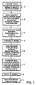
- Fig. 1 is a process flow diagram depicting the steps of the method of the invention; and
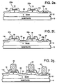
- Figs. 2a-2g are each a cross-sectional view, not to scale, showing the fabrication of a photodiode array in accordance with the method of the invention.
-
- Although described below in the context of a fabrication process for PV detectors having a mesa geometry, it should be realized that the teaching of the invention is applicable also to planar arrays of PV detectors, and also to the fabrication of photoconductive (PC) IR detectors comprised of Group IIB-VIA semiconductor material.
- Reference is made to the process flow diagram of Fig. 1, in conjunction with the various cross-sectional views of Figs. 2a-2g. In Figs. 2a-2g a portion of an array, specifically two mesa structures, is shown. It should be realized that a typical array of radiation detectors would comprise a significantly larger number of mesa structures arranged in a linear or a two-dimensional array.
- (Fig. 1 - Block A) Processing begins with an n-type radiation absorbing
HgCdTe base layer 12 that is grown on an electrically insulating andtransparent substrate 10.Substrate 10 is selected to be transparent at wavelengths of interest, specifically those wavelengths that are desired to be absorbed within thebase layer 12. A preferred method for growing thebase layer 12 on thesubstrate 10 is by Liquid Phase Epitaxy (LPE), although Molecular Beam Epitaxy (MBE) and Metal-Organic Chemical Vapor Deposition (MOCVD) are also suitable growth techniques. A suitable material for thesubstrate 10 is CdZnTe. The bandgap of the HgCdTe semiconductor material of thebase layer 12 is selected for absorbing radiation having the wavelengths of interest and is set, in a known fashion, by varying the relative concentrations of the Hg and Cd atoms in accordance with the formula: Hg(1-x)Cd(x)Te, wherein (x) is a nonzero number that is less than one. Upon thebase layer 12 is then epitaxially grown a p-type HgCdTe cap layer 14. The cap layer 14 may be grown, by example, by LPE, MBE, or by MOCVD. A suitable dopant species for thebase layer 12 is indium having a concentration of approximately 1015 atoms/cm3. A suitable dopant species for the cap layer 14 is arsenic having a concentration of approximately 1018 atoms/cm3. Individual photodiodes are delineated by a mesa etch process, using bromine/ethyleneglycol or bromine/methanol, in conjunction with a photolithographically applied mask. The result of the mesa etch is to differentiate the p-type cap layer into a plurality of electricallyisolated regions 14a, each of theregions 14a being contained within a mesa and forming a p-n junction with the underlying n-type base layer 12. - (Fig. 1 - Block B, Fig. 2b) A next step of the method applies, to each of the
cap layers 14a, ametal contact pad 16. Acommon contact pad 18 is also applied to the n-typeHgCdTe base layer 12. In accordance with an aspect of the invention, the metal contact pad is comprised of a refractory metal selected to have a low diffusion characteristic, at elevated temperatures, so as to prevent the diffusion of the contact metal into the underlyingHgCdTe cap layer 14a. A presently preferred metal is Mo. A further advantage of Mo is that it exhibits a CTE that is more closely matched to the HgCdTe than is the CTE of many commonly used contact metals, such as Cr and Au. As a result, when the structure is heated the Mo contacts tend not to exert undesirable stresses on the underlying semiconductor material. A presently preferred technique deposits the Mo contact metalization by sputter deposition and a lift-off process. A suitable thickness for thecontact pads - (Fig. 1 - Block C, Fig. 2c) A next step overcoats the structure formed thus far with a
layer 20 of wide bandgap Group IIB-VIA semiconductor material. This wide bandgap semiconductor material may be, by example, CdTe, CdZnTe, or CdSeTe. A presently preferred technique is to blanket deposit CdTe to a depth of approximately 4 x 10⁻⁷ metres (4000 Angstroms) by a thermal evaporation process. Other suitable deposition techniques include MBE, MOCVD, and sputtering. As can be seen in Fig. 2c, the effect of this step is to cover the exposed surface of the n-type base layer 12, the exposed surfaces of the p-type cap layers 14a, and also theMo contacts - (Fig. 1 - Block D, Fig. 2d) A next step anneals the structure formed thus far in Hg vapor at a first temperature for a first period of time and then at a second, lower temperature for a second period of time. In general, both the first and the second temperatures are greater than a temperature used during a subsequent Dewar bake-out process. That is, both the first and the second temperatures are greater than approximately 150°C. One result of the anneal is to interchange Hg and Cd at cation sites along an interface between the
layers layer 20. This interface region is shown in Fig. 2d in a crosshatched manner. - (Fig. 1 - Block E, Fig. 2e) After annealing the structure,
windows 20a are opened through thelayer 20 to expose theMo contacts windows 20a is to employ photoresist patterning in conjunction with a wet chemical etch. Two suitable wet etchants are Br/ethyleneglycol and Br/methanol. Thewindows 20a may also be opened by ion beam milling or by a reactive ion etch process. TheMo contacts windows 20a. - (Fig. 1 - Block F, Fig. 2f) The structure is next overcoated with a
dielectric layer 22 comprised of, by example, Si3N4, SiO2, or SiO. A suitable method for depositing thedielectric layer 22 is by a plasma process that deposits the layer to a thickness of approximately 1 x 10⁻⁷ metres (1000 Angstroms). Next, a photoresist patterning step provides an apertured mask, andwindows 22a are opened through thedielectric layer 22 to expose theMo contacts windows 22a is to employ photoresist patterning with a wet chemical etch. CF4 is one suitable wet etchant. The photoresist mask is stripped after opening thewindows 22a. - (Fig. 1 - Block G, Fig. 2g) The structure is photolithographically patterned to provide an indium bump mask, and indium bumps 24 are applied to contact individual ones of the photodiode
Mo contact pads 16, and to the common Mo contact pad(s) 18, through thewindows 22a. One suitable method forms the indium bumps 24 to a thickness of approximately 12 microns through the use of a thermal evaporation technique. As can be seen in Fig. 2g, as a result of this step only the In bumps 24 are left exposed, with the underlying Mo contact metallization being buried beneath thedielectric layer 22. Thedielectric layer 22, or overglass, is also substantially impervious to the passage of Hg, and thus beneficially prevents the out-diffusion of Hg from thebase layer 12 and theregions 14a. - (Fig. 1 - Block H) At some subsequent time the array of PV diodes thus formed is mated to, or hybridized with, a readout circuit through the In bumps 24. Prior to joining the array to the readout circuit the In bumps 24 are chemically wet etched to remove any surface oxides that would adversely affect the contact resistance. An etching procedure such as that described in the aforementioned commonly assigned U.S. Patent No. 4,865,245, issued to E.F. Schulte et al., may be employed.
- In accordance with an aspect of the invention only the In bumps 24 are exposed to the etchant, the underlying contact metallization being buried beneath the
dielectric layer 22. As a result, the aforementioned problems resulting from the proximity of two dissimilar metals are overcome, the In bumps 24 are uniformly etched over the surface of the array, and In-Te whiskers are not produced. The use of the method of the invention thus improves the yield of IR detector arrays by improving theIn bump 24 quality during the hybridization process, and also improves reliability by ensuring that the size and shape of the In bumps 24 is maintained at their design dimensions. - In accordance with another aspect of the invention, the anneal in Fig. 2d is performed with a
CdTe layer 20 that is substantially continuous across the entire surface of the array. This overcomes the above noted problem that results from annealing with an etched CdTe film. That is, localized stresses in the underlying HgCdTe material, associated with openings in the CdTe film, are not generated. - It has been found that arrays of PV diodes fabricated in accordance with the invention exhibit stable performance after a 74 hour vacuum bake (Dewar bake-out) at 145°C. Heretofore, bake temperatures have been limited to 100°C or less because of the above mentioned instabilities in the surface passivation and/or the diffusion of the contact metal into the HgCdTe. Also, in that both the
passivation layer 20 and the Mo contact metal were previously annealed at a substantially higher temperature, neither is expected to change significantly at storage or processing temperatures that are less than the anneal temperature. - It should be realized that although the invention has been described in the context of specific materials, specific dimensions, and specific processing parameters, such as etchants and deposition techniques, a number of modifications to these various materials, dimensions, and processing parameters may be made, while still obtaining the same result. Furthermore, the teaching of the invention is also applicable to n-on-p devices and also to photoconductive, as opposed to photovoltaic, devices. The teaching of the invention is also applicable to photoresponsive devices having a planar configuration, wherein a p-n junction is formed within a body of HgCdTe through a diffusion or implantation of an acceptor or a donor species into the body.
Claims (13)
- A method for fabricating a photovoltaic diode, comprising in the following order the steps of:providing a p-n junction between a base layer (12), grown on a substrate (10) and comprised of Group IIB-VIA semiconductor material having a first type of electrical conductivity, and a cap region (14a) comprised of Group IIB-VIA semiconductor material having a second type of electrical conductivity;forming a metal contact electrode (16) upon the cap region (14a);coating the base layer (12), the cap region (14a), and the metal contact electrode (16) to form a coated structure, the step of coating including a step of depositing a first coating layer (20) comprised of a semiconductor material having a bandgap selected to be wider than a bandgap of the semiconductor material of either the base layer (12) or the cap region (14a);thermally annealing the coated structure;opening a first window (20a) through the first coating layer (20) for exposing, within the first window, a surface of the metal contact electrode (16); andforming an electrically conductive interconnection (24) to the metal contact electrode (16) for contacting an external circuit, including the steps of:coating exposed surfaces of the first coating layer (20), the first window (20a), and the metal contact electrode (16) with a second coating layer (22) comprised of a dielectric material;opening a second window (22a) through the second coating layer (22) in registration with the first window (20a) for exposing, within the second window (22a), the surface of the metal contact electrode (16); andforming the electrically conductive interconnection (24) within the second window (22a) and on the exposed surface of the metal contact electrode (16) such that only a portion of the electrically conductive interconnection (24) is exposed, and no portion of the underlying metal contact electrode (16) is exposed.
- A method as set forth in claim 1, wherein the step of providing a p-n junction includes the steps of:providing the base layer (12) comprised of Group IIB-VIA semiconductor material having the first type of electrical conductivity, the base layer (12) having an overlying cap layer of Group IIB-VIA semiconductor material having the second type of electrical conductivity; anddifferentiating the cap layer into a plurality of electrically isolated regions for forming a plurality of mesa structures, each of the mesa structures including an interface between the base layer (12) and one of the electrically isolated regions for forming the p-n junction.
- A method as set forth in claim 2, wherein said base layer (12) is comprised of n-type HgCdTe and wherein said cap layer is comprised of p-type HgCdTe.
- A method as set forth in either of claims 1 or 2, wherein the step of forming a metal contact electrode (16) upon the cap region (14a) forms the metal contact electrode (16) with a metal selected to have a coefficient of thermal expansion that is similar to that of the cap region (14a), the metal also being selected to have a low diffusivity into the cap region (14a).
- A method as set forth in any preceding claim, wherein the step of coating the base layer (12), the cap region (14a), and the metal contact electrode (16) includes a step of depositing a layer of semiconductor material selected from the group consisting of CdTe, CdSeTe, and CdZnTe.
- A method as set forth in any preceding claim, wherein the step of coating exposed surfaces of the first coating layer (20), the first window (20a) and the metal contact electrode (16) with a second coating layer (22) comprised of a dielectric material includes depositing a layer of a material selected from the group consisting of SiO2, SiO and Si3N4.
- A method as set forth in any preceding claim, wherein the step of thermally annealing the coated structure occurs in a mercury vapor, and includes the steps of:providing a first temperature for a first period of time; andproviding a second, lower temperature for a second period of time.
- A photodiode, comprising:wherein said dielectric layer (22) is in intimate contact with side surfaces of said interconnect (24) such that no portion of said metal contact electrode (16) may be physically contacted from a top surface of said dielectric layer (22).a substrate (10);a semiconductor base region (12) overlying the substrate (10) and comprising elements selected from Group IIB-VIA, said base region (12) having a first type of electrical conductivity;a semiconductor cap region (14a) disposed upon said base region (12), said cap region (14a) being comprised of elements selected from Group IIB-VIA, said cap region (14a) having a second type of electrical conductivity and forming a p-n junction with said base region (12);an electrically conductive metal contact electrode (16) formed upon a top surface of said cap region (14a);a semiconductor layer (20) overlying said base region (12), said cap region (14a), and also partially overlying said metal contact electrode (16), the semiconductor layer (20) comprising elements selected from Group IIB-VIA, said semiconductor layer (20) having a wider bandgap than a bandgap of said base region (12) and said cap region (14a);a dielectric layer (22) overlying said semiconductor layer (20); andan electrically conductive interconnect (24) formed upon said metal contact electrode (16), said interconnect (24) extending upwardly from said metal contact electrode (16) and through said dielectric layer (22);
- A photodiode as set forth in claim 8, wherein said substrate (10) is comprised of elements selected from Group IIB-VIA.
- A photodiode as set forth in claim 8 and further comprising:a second electrically conductive metal contact pad (18) formed upon a top surface of said base region (12); anda second electrically conductive interconnect (24) formed upon said second metal contact pad (18), said second interconnect (24) extending upwardly from said second metal contact pad (18) and through said dielectric layer (22), wherein said dielectric layer (22) is in intimate contact with side surfaces of said second interconnect (24) such that no portion of said second metal contact pad (18) is accessible from the top surface of said dielectric layer (22).
- A photodiode as set forth in any one of claims 8 to 10, wherein said base region (12) is comprised of n-type HgCdTe, and wherein said cap region (14a) is comprised of p-type HgCdTe.
- A photodiode as set forth in any one of claims 8 to 11, wherein said semiconductor layer (20) is comprised of material selected from the group consisting of CdTe, CdSeTe, and CdZnTe.
- A photodiode as set forth in any one of claims 8 to 12, wherein said dielectric layer (22) is comprised of material selected from the group consisting of SiO2, SiO, and Si3N4.
Priority Applications (4)
| Application Number | Priority Date | Filing Date | Title |
|---|---|---|---|
| US07/917,562 US5296384A (en) | 1992-07-21 | 1992-07-21 | Bake-stable HgCdTe photodetector and method for fabricating same |
| DE69332060T DE69332060T2 (en) | 1993-07-22 | 1993-07-22 | Glow-resistant HgCdTe photodetector and manufacturing process |
| EP93305794A EP0635892B1 (en) | 1992-07-21 | 1993-07-22 | Bake-stable HgCdTe photodetector and method for fabricating same |
| US08/270,527 US5401986A (en) | 1992-07-21 | 1994-07-05 | Bake-stable HgCdTe photodetector with II-VI passivation layer |
Applications Claiming Priority (3)
| Application Number | Priority Date | Filing Date | Title |
|---|---|---|---|
| US07/917,562 US5296384A (en) | 1992-07-21 | 1992-07-21 | Bake-stable HgCdTe photodetector and method for fabricating same |
| EP93305794A EP0635892B1 (en) | 1992-07-21 | 1993-07-22 | Bake-stable HgCdTe photodetector and method for fabricating same |
| US08/270,527 US5401986A (en) | 1992-07-21 | 1994-07-05 | Bake-stable HgCdTe photodetector with II-VI passivation layer |
Publications (2)
| Publication Number | Publication Date |
|---|---|
| EP0635892A1 EP0635892A1 (en) | 1995-01-25 |
| EP0635892B1 true EP0635892B1 (en) | 2002-06-26 |
Family
ID=27235453
Family Applications (1)
| Application Number | Title | Priority Date | Filing Date |
|---|---|---|---|
| EP93305794A Expired - Lifetime EP0635892B1 (en) | 1992-07-21 | 1993-07-22 | Bake-stable HgCdTe photodetector and method for fabricating same |
Country Status (2)
| Country | Link |
|---|---|
| US (1) | US5401986A (en) |
| EP (1) | EP0635892B1 (en) |
Cited By (2)
| Publication number | Priority date | Publication date | Assignee | Title |
|---|---|---|---|---|
| US11851785B2 (en) | 2021-05-21 | 2023-12-26 | Raytheon Company | Aluminum nitride passivation layer for mercury cadmium telluride in an electrical device |
| US11894477B2 (en) | 2021-05-17 | 2024-02-06 | Raytheon Company | Electrical device with stress buffer layer and stress compensation layer |
Families Citing this family (18)
| Publication number | Priority date | Publication date | Assignee | Title |
|---|---|---|---|---|
| GB2289983B (en) | 1994-06-01 | 1996-10-16 | Simage Oy | Imaging devices,systems and methods |
| US5942788A (en) * | 1995-05-09 | 1999-08-24 | Minolta Co., Ltd. | Solid state image sensing device |
| US5846850A (en) * | 1995-09-05 | 1998-12-08 | Raytheon Ti Systems, Inc. | Double sided interdiffusion process and structure for a double layer heterojunction focal plane array |
| US5646426A (en) * | 1995-12-12 | 1997-07-08 | Santa Barbara Research Center | Contact metal diffusion barrier for semiconductor devices |
| US5998235A (en) * | 1997-06-26 | 1999-12-07 | Lockheed Martin Corporation | Method of fabrication for mercury-based quaternary alloys of infrared sensitive materials |
| US9029793B2 (en) | 1998-11-05 | 2015-05-12 | Siemens Aktiengesellschaft | Imaging device |
| DE10037103A1 (en) * | 2000-07-27 | 2002-02-14 | Aeg Infrarot Module Gmbh | Multispectral photodiode |
| JP4208172B2 (en) * | 2000-10-31 | 2009-01-14 | シャープ株式会社 | Photodiode and light receiving element with built-in circuit using the same |
| US6803322B1 (en) * | 2000-12-15 | 2004-10-12 | Science Applications International Corporation | Pin alloy-semiconductor, radiation detectors with rectifying junction contacts, methods and systems for forming pin alloy-semiconductor devices with rectifying junction contacts, and systems and methods for analyzing alloy-semiconductor properties |
| GB0224689D0 (en) | 2002-10-23 | 2002-12-04 | Simage Oy | Formation of contacts on semiconductor substrates |
| JP2006504258A (en) | 2002-10-25 | 2006-02-02 | ゴールドパワー リミテッド | Circuit board and manufacturing method thereof |
| FR2869462B1 (en) * | 2004-04-21 | 2006-06-02 | Fr De Detecteurs Infrarouges S | METHOD FOR PRODUCING AN ELECTROMAGNETIC RADIATION DETECTOR, IN PARTICULAR INFRARED |
| KR100723457B1 (en) * | 2006-09-20 | 2007-05-31 | (주)한비젼 | A semiconductor device |
| US7544532B2 (en) * | 2006-10-17 | 2009-06-09 | Raytheon Company | Infrared photodiodes and sensor arrays with improved passivation layers and methods of manufacture |
| CN100541146C (en) * | 2007-04-25 | 2009-09-16 | 中国科学院上海技术物理研究所 | The cadmium-telluride-mercury infrared detector chip of anti-non-infrared radiation incidence plane response |
| DE102013214575B3 (en) * | 2013-07-25 | 2014-09-18 | Siemens Aktiengesellschaft | Semiconductor element with Lötstopplage and method for its production and radiation detector and medical device with such a radiation detector |
| CN110416324A (en) * | 2019-08-22 | 2019-11-05 | 浙江正泰太阳能科技有限公司 | A kind of solar battery and preparation method thereof |
| US20220416095A1 (en) * | 2021-06-29 | 2022-12-29 | Raytheon Company | Low-stress dielectric layer, planarization method, and low-temperature processing for 3d-integrated electrical device |
Family Cites Families (28)
| Publication number | Priority date | Publication date | Assignee | Title |
|---|---|---|---|---|
| FR2168934B1 (en) * | 1972-01-27 | 1977-04-01 | Telecommunications Sa | |
| FR2281650A1 (en) * | 1974-08-06 | 1976-03-05 | Telecommunications Sa | PROCESS FOR MANUFACTURING A PHOTODIODE SENSITIVE TO INFRARED RADIATION AND PHOTODIODE OBTAINED BY THIS PROCESS |
| US4000508A (en) * | 1975-07-17 | 1976-12-28 | Honeywell Inc. | Ohmic contacts to p-type mercury cadmium telluride |
| FR2336804A1 (en) * | 1975-12-23 | 1977-07-22 | Telecommunications Sa | IMPROVEMENTS MADE TO SEMICONDUCTOR DEVICES, ESPECIALLY TO PHOTOVOLTAIC DETECTORS INCLUDING A SUBSTRATE BASED ON A CDXHG1-XTE ALLOY, AND PROCESS FOR MANUFACTURING SUCH A PERFECTED DEVICE |
| US4206003A (en) * | 1977-07-05 | 1980-06-03 | Honeywell Inc. | Method of forming a mercury cadmium telluride photodiode |
| DE2739309A1 (en) * | 1977-09-01 | 1979-03-15 | Licentia Gmbh | Infrared detector cell - pref. based on cadmium mercury telluride or lead tin telluride semiconductors with getter layers |
| USRE30412E (en) * | 1979-04-26 | 1980-10-07 | Eastman Kodak Company | CdTe Barrier type photovoltaic cells with enhanced open-circuit voltage, and process of manufacture |
| FR2488048A1 (en) * | 1980-07-30 | 1982-02-05 | Telecommunications Sa | SENSITIVE PHOTOVOLTAIC DETECTOR IN NEAR INFRARED |
| DE3278553D1 (en) * | 1981-06-24 | 1988-06-30 | Secr Defence Brit | Photo diodes |
| US4439912A (en) * | 1982-04-19 | 1984-04-03 | The United States Of America As Represented By The Secretary Of The Army | Infrared detector and method of making same |
| US4549195A (en) * | 1983-04-14 | 1985-10-22 | Westinghouse Electric Corp. | Heterojunction semiconductor device |
| JPS603165A (en) * | 1983-06-20 | 1985-01-09 | Matsushita Electric Ind Co Ltd | Light-receiving element |
| US4611091A (en) * | 1984-12-06 | 1986-09-09 | Atlantic Richfield Company | CuInSe2 thin film solar cell with thin CdS and transparent window layer |
| US4639756A (en) * | 1986-05-05 | 1987-01-27 | Santa Barbara Research Center | Graded gap inversion layer photodiode array |
| FR2604298B1 (en) * | 1986-09-19 | 1988-10-28 | Commissariat Energie Atomique | PROCESS FOR MAKING AN ELECTRICAL CONTACT TAKING ON A SUBSTRATE IN P-CONDUCTIVITY HGCDTE AND APPLICATION TO THE MANUFACTURE OF A N / P DIODE |
| US4764261A (en) * | 1986-10-31 | 1988-08-16 | Stemcor Corporation | Method of making improved photovoltaic heterojunction structures |
| US4735662A (en) * | 1987-01-06 | 1988-04-05 | The Standard Oil Company | Stable ohmic contacts to thin films of p-type tellurium-containing II-VI semiconductors |
| US4865245A (en) * | 1987-09-24 | 1989-09-12 | Santa Barbara Research Center | Oxide removal from metallic contact bumps formed on semiconductor devices to improve hybridization cold-welds |
| US4818565A (en) * | 1987-10-30 | 1989-04-04 | Regents Of The University Of Minnesota | Method to stabilize metal contacts on mercury-cadmium-telluride alloys |
| JPH01223779A (en) * | 1988-03-03 | 1989-09-06 | Toshiba Corp | Infrared ray detector |
| JP2670289B2 (en) * | 1988-03-31 | 1997-10-29 | 株式会社東芝 | Infrared detecting photodiode and method for manufacturing the same |
| US5189297A (en) * | 1988-08-29 | 1993-02-23 | Santa Barbara Research Center | Planar double-layer heterojunction HgCdTe photodiodes and methods for fabricating same |
| US5144138A (en) * | 1989-10-06 | 1992-09-01 | Texas Instruments Incorporated | Infrared detector and method |
| JPH03196683A (en) * | 1989-12-26 | 1991-08-28 | Nec Corp | Infrared ray detector made of mercury cadmium telluride |
| US5149956A (en) * | 1991-06-12 | 1992-09-22 | Santa Barbara Research Center | Two-color radiation detector array and methods of fabricating same |
| US5192695A (en) * | 1991-07-09 | 1993-03-09 | Fermionics Corporation | Method of making an infrared detector |
| JP2809908B2 (en) * | 1991-09-30 | 1998-10-15 | 三菱電機株式会社 | Solid-state imaging device |
| US5279974A (en) * | 1992-07-24 | 1994-01-18 | Santa Barbara Research Center | Planar PV HgCdTe DLHJ fabricated by selective cap layer growth |
-
1993
- 1993-07-22 EP EP93305794A patent/EP0635892B1/en not_active Expired - Lifetime
-
1994
- 1994-07-05 US US08/270,527 patent/US5401986A/en not_active Expired - Lifetime
Cited By (2)
| Publication number | Priority date | Publication date | Assignee | Title |
|---|---|---|---|---|
| US11894477B2 (en) | 2021-05-17 | 2024-02-06 | Raytheon Company | Electrical device with stress buffer layer and stress compensation layer |
| US11851785B2 (en) | 2021-05-21 | 2023-12-26 | Raytheon Company | Aluminum nitride passivation layer for mercury cadmium telluride in an electrical device |
Also Published As
| Publication number | Publication date |
|---|---|
| EP0635892A1 (en) | 1995-01-25 |
| US5401986A (en) | 1995-03-28 |
Similar Documents
| Publication | Publication Date | Title |
|---|---|---|
| EP0635892B1 (en) | Bake-stable HgCdTe photodetector and method for fabricating same | |
| US4070689A (en) | Semiconductor solar energy device | |
| US4972244A (en) | Photodiode and photodiode array on a II-VI material and processes for the production thereof | |
| US6657194B2 (en) | Multispectral monolithic infrared focal plane array detectors | |
| US3508126A (en) | Semiconductor photodiode with p-n junction spaced from heterojunction | |
| US5185648A (en) | Plural-wavelength infrared detector devices | |
| US4949144A (en) | Semiconductor photo-detector having a two-stepped impurity profile | |
| US4897123A (en) | Solar cells and method for producing solar cells | |
| US4665609A (en) | Process of manufacturing a photosensitive device having a plurality of detectors separated by zones impervious to the radiation to be detected | |
| US5189297A (en) | Planar double-layer heterojunction HgCdTe photodiodes and methods for fabricating same | |
| EP0068652B1 (en) | Photo diodes | |
| CA1294349C (en) | Rear entry photodiode | |
| US5279974A (en) | Planar PV HgCdTe DLHJ fabricated by selective cap layer growth | |
| US5608255A (en) | FET optical receiver using backside illumination, indium materials species | |
| US20030102432A1 (en) | Monolithic infrared focal plane array detectors | |
| US4956304A (en) | Buried junction infrared photodetector process | |
| US5751049A (en) | Two-color infrared detector | |
| US5296384A (en) | Bake-stable HgCdTe photodetector and method for fabricating same | |
| US4875082A (en) | Schottky barrier photodiode structure | |
| US5646426A (en) | Contact metal diffusion barrier for semiconductor devices | |
| US4742017A (en) | Implantation method for forming Schottky barrier photodiodes | |
| US5599733A (en) | Method using cadmium-rich CdTe for lowering the metal vacancy concentrations of HgCdTe surfaces | |
| KR100422294B1 (en) | Passivation of HgCdTe Junction Diode By Annealing In Cd/Hg Atmosphere | |
| US5187378A (en) | Photodetector | |
| IL106458A (en) | Bake-stable HgCdTe photodetector and method for fabricating same |
Legal Events
| Date | Code | Title | Description |
|---|---|---|---|
| PUAI | Public reference made under article 153(3) epc to a published international application that has entered the european phase |
Free format text: ORIGINAL CODE: 0009012 |
|
| AK | Designated contracting states |
Kind code of ref document: A1 Designated state(s): DE ES FR GB IT NL |
|
| 17P | Request for examination filed |
Effective date: 19950630 |
|
| 17Q | First examination report despatched |
Effective date: 19971031 |
|
| RAP1 | Party data changed (applicant data changed or rights of an application transferred) |
Owner name: RAYTHEON COMPANY |
|
| GRAG | Despatch of communication of intention to grant |
Free format text: ORIGINAL CODE: EPIDOS AGRA |
|
| GRAG | Despatch of communication of intention to grant |
Free format text: ORIGINAL CODE: EPIDOS AGRA |
|
| GRAH | Despatch of communication of intention to grant a patent |
Free format text: ORIGINAL CODE: EPIDOS IGRA |
|
| GRAH | Despatch of communication of intention to grant a patent |
Free format text: ORIGINAL CODE: EPIDOS IGRA |
|
| GRAA | (expected) grant |
Free format text: ORIGINAL CODE: 0009210 |
|
| AK | Designated contracting states |
Kind code of ref document: B1 Designated state(s): DE ES FR GB IT NL |
|
| PG25 | Lapsed in a contracting state [announced via postgrant information from national office to epo] |
Ref country code: NL Free format text: LAPSE BECAUSE OF FAILURE TO SUBMIT A TRANSLATION OF THE DESCRIPTION OR TO PAY THE FEE WITHIN THE PRESCRIBED TIME-LIMIT Effective date: 20020626 |
|
| REG | Reference to a national code |
Ref country code: GB Ref legal event code: FG4D |
|
| REF | Corresponds to: |
Ref document number: 69332060 Country of ref document: DE Date of ref document: 20020801 |
|
| ET | Fr: translation filed | ||
| NLV1 | Nl: lapsed or annulled due to failure to fulfill the requirements of art. 29p and 29m of the patents act | ||
| PG25 | Lapsed in a contracting state [announced via postgrant information from national office to epo] |
Ref country code: ES Free format text: LAPSE BECAUSE OF FAILURE TO SUBMIT A TRANSLATION OF THE DESCRIPTION OR TO PAY THE FEE WITHIN THE PRESCRIBED TIME-LIMIT Effective date: 20021220 |
|
| PLBE | No opposition filed within time limit |
Free format text: ORIGINAL CODE: 0009261 |
|
| STAA | Information on the status of an ep patent application or granted ep patent |
Free format text: STATUS: NO OPPOSITION FILED WITHIN TIME LIMIT |
|
| 26N | No opposition filed |
Effective date: 20030327 |
|
| PGFP | Annual fee paid to national office [announced via postgrant information from national office to epo] |
Ref country code: GB Payment date: 20050615 Year of fee payment: 13 |
|
| PGFP | Annual fee paid to national office [announced via postgrant information from national office to epo] |
Ref country code: DE Payment date: 20050617 Year of fee payment: 13 |
|
| PG25 | Lapsed in a contracting state [announced via postgrant information from national office to epo] |
Ref country code: GB Free format text: LAPSE BECAUSE OF NON-PAYMENT OF DUE FEES Effective date: 20060722 |
|
| PGFP | Annual fee paid to national office [announced via postgrant information from national office to epo] |
Ref country code: IT Payment date: 20060731 Year of fee payment: 14 |
|
| PG25 | Lapsed in a contracting state [announced via postgrant information from national office to epo] |
Ref country code: DE Free format text: LAPSE BECAUSE OF NON-PAYMENT OF DUE FEES Effective date: 20070201 |
|
| GBPC | Gb: european patent ceased through non-payment of renewal fee |
Effective date: 20060722 |
|
| PG25 | Lapsed in a contracting state [announced via postgrant information from national office to epo] |
Ref country code: IT Free format text: LAPSE BECAUSE OF NON-PAYMENT OF DUE FEES Effective date: 20070722 |
|
| PGFP | Annual fee paid to national office [announced via postgrant information from national office to epo] |
Ref country code: FR Payment date: 20120719 Year of fee payment: 20 |