EP0068652A2 - Photodioden - Google Patents
Photodioden Download PDFInfo
- Publication number
- EP0068652A2 EP0068652A2 EP82302843A EP82302843A EP0068652A2 EP 0068652 A2 EP0068652 A2 EP 0068652A2 EP 82302843 A EP82302843 A EP 82302843A EP 82302843 A EP82302843 A EP 82302843A EP 0068652 A2 EP0068652 A2 EP 0068652A2
- Authority
- EP
- European Patent Office
- Prior art keywords
- cdte
- type
- photo diode
- layer
- substrate
- Prior art date
- Legal status (The legal status is an assumption and is not a legal conclusion. Google has not performed a legal analysis and makes no representation as to the accuracy of the status listed.)
- Granted
Links
Images
Classifications
-
- H—ELECTRICITY
- H10—SEMICONDUCTOR DEVICES; ELECTRIC SOLID-STATE DEVICES NOT OTHERWISE PROVIDED FOR
- H10F—INORGANIC SEMICONDUCTOR DEVICES SENSITIVE TO INFRARED RADIATION, LIGHT, ELECTROMAGNETIC RADIATION OF SHORTER WAVELENGTH OR CORPUSCULAR RADIATION
- H10F39/00—Integrated devices, or assemblies of multiple devices, comprising at least one element covered by group H10F30/00, e.g. radiation detectors comprising photodiode arrays
- H10F39/10—Integrated devices
- H10F39/12—Image sensors
- H10F39/18—Complementary metal-oxide-semiconductor [CMOS] image sensors; Photodiode array image sensors
- H10F39/184—Infrared image sensors
-
- H—ELECTRICITY
- H10—SEMICONDUCTOR DEVICES; ELECTRIC SOLID-STATE DEVICES NOT OTHERWISE PROVIDED FOR
- H10F—INORGANIC SEMICONDUCTOR DEVICES SENSITIVE TO INFRARED RADIATION, LIGHT, ELECTROMAGNETIC RADIATION OF SHORTER WAVELENGTH OR CORPUSCULAR RADIATION
- H10F39/00—Integrated devices, or assemblies of multiple devices, comprising at least one element covered by group H10F30/00, e.g. radiation detectors comprising photodiode arrays
- H10F39/011—Manufacture or treatment of image sensors covered by group H10F39/12
- H10F39/016—Manufacture or treatment of image sensors covered by group H10F39/12 of thin-film-based image sensors
Definitions
- This invention relates to photo diodes.
- a photo diode is a two terminal semiconductor device having one terminal attached to a piece of p-type material and the other terminal connected to a piece of n-type material with a p-n junction between the two types of materials. An electron flow occurs across the p-n junction when illuminated by electro magnetic radiation of a suitable wavelength.
- One known photo diode comprises a substrate of p-type Cd x Hg 1-x Te (C.M.T.) on which a layer of ZnS has been grown. This is described e.g. in App. Phy. Letts. 34(1) 1 Jan. 1979, pages 50-52, M Lanir et al. A p-n junction is formed in the bulk of the CdHgTe by ion implantation through the ZnS. Such a device is sensitive to infra red radiation and is therefore useful in thermal imaging systems where the thermal image of a scene is measured and used to form a visible display on a cathode ray tube.
- C.M.T. p-type Cd x Hg 1-x Te
- an infra red sensitive photo diode comprises a piece of Cd x Hg 1-x Te and a piece of CdTe forming a p-n junction with terminals connected to the p and n type materials.
- the Cd x Hg 1-x Te may be p-type in which case the CdTe is n-type or vice versa.
- the n-type CdTe may be grown as a semi-insulating layer with a layer of a group IIIa or VII donor dopant deposited on top and diffused into the CdTe to form n-type CdTe.
- the dopant may be In.
- a p-type CdTe layer may be grown in a similar manner using as dopants P, As, Ag, or Au.
- the CdTe may be grown n-type by molecular beam epitaxial techniques with an In dopant.
- areas of C.M.T. not forming diode junctions may be passivated by a layer of semi-insulating CdTe.
- the CdTe layers may be grown by an suitable epitaxial growth technique, e.g. M.B.E., vapour-growth, etc.
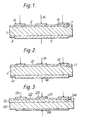
- the substrate 1 is cut, cleaned, and polished and placed in a molecular beam epitaxial (M.B.E.) growth chamber where a protective passivating layer 2, 3 of CdTe is grown on all surfaces.
- Typical layer 2 thickness on top of the substrate 1 is 0.5 ⁇ m in a range of about 0.2 to 1 ⁇ m. Islands 4 of In are deposited, e.g. by evaporation, on the top surface of CdTe 2.
- the structure is then heated typically at 70-120°C for 4 to 40 hours to diffuse In into the CdTe 2 giving n-type heavily doped regions 8 (e.g. number of electrons, n > 5 ⁇ 10 16 cm -3 ) under the islands 4. Additionally this heating causes inter diffusion at the C.M.T. and CdTe interface (p-n junction 7) with Hg diffusing into the CdTe layer 2 and Cd diffusing into the C.M.T. This gives a gradual material composition change creating a graded heterostructure where the p-n junction is close to the heterojunction.
- a back electrode 5, e.g. of Au, is formed through apertures in the bottom CdTe layer direct onto the substrate.
- a top terminal connection 6 is made separately to each In island 4.
- the C.M.T. substrate can be thick in which case no passivation of the bottom surface is necessary although it may be applied as above.
- Infra red radiation incident on the p-n junction 7 causes a measurable voltage or current flow (dependent on the external circuitry) to be developed at the terminals 5, 6.
- Figure 2 shows an alternative form of photo diode array comprising a p-type Cd x Hg 1-x Te substrate 11 with islands 12 of n-type doped'CdTe. Between the islands 12 is a layer 13 of semi-insulating CdTe. A passivating layer 14 of CdTe covers the remaining substrate surfaces.
- the n-type CdTe material 12 is grown in a molecular beam epitaxial chamber using an In dopant source in addition to the Cd, and Te sources. Alternatively the stoichiometry of the CdTe layer may be adjusted to give semi-insulating or semi-conducting layers. Photolithographic techniques are used to define the different parts of the top layer. For example islands of photo resist may be formed on the top surface of the substrate. A semi-insulating layer of CdTe is grown over the islands and top of the substrate. The resist is then lifted off leaving apertures through which n-type CdTe is grown.
- Terminal connections 15, 16 are made to each island and the bottom of the substrate 11 as before.
- the structure is heated e.g. at 70-120 C for 4-40 hours to allow diffusion at the p-n junction 17 as before.
- the composition of the n-type CdTe may be changed during molecular beam epitaxial growth.
- the alloy Cd x Hg 1-x Te may be grown initially and the Hg source gradually reduced until only doped CdTe is being grown.
- Such a graded composition may also be used in the device of Figure 1.
- Figure 3 shows another form of photo diode array. It comprises a p-type semi-conducting substrate 20 of CdTe on which a p-type layer 21 of Cd x Hg 1-x Te is grown (or polished, lapped) to a typical thickness of 10 to 30 ym.
- a semi-insulating layer of CdTe 22 is grown on the layer and islands 23 of In deposited on the CdTe 22 as in Figure 1. As before the device is heated to diffuse the In 23 into the CdTe layer 27, and also cause a diffusion at the p-n junction 24. Terminals 25, 26 are connected top and bottom as before.
- the CdTe 20 may be grown on a supporting base of other suitable material by M.B.E.
- an electrode 26 on the rear surface electrodes may be arranged on the top surface of the C.M.T. 21 to one side of the islands 23.
- the C.M.T. 21 may be grown by liquid, vapour, or molecular beam epitaxial techniques or using alkyls of Cd and Te flowing over the CdTe substrate 20 in an atmosphere of Hg. Such a technique is described in U.K. Patent Application No. 2,078,695 A, U.S.A. Patent Application Serial No. 266,046.
- the n-type CdTe of Figure 3 may alternatively be formed as in Figure 2 using In doped and molecular beam epitaxial techniques.
- the CdTe layer may be selectively n-type doped by implantation of In ions.
- the CdTe layer may be formed with a graded composition i.e. starting by growing C.M.T. and gradually reducing the Hg source.
Landscapes
- Light Receiving Elements (AREA)
- Solid State Image Pick-Up Elements (AREA)
Applications Claiming Priority (2)
| Application Number | Priority Date | Filing Date | Title |
|---|---|---|---|
| GB8119440 | 1981-06-23 | ||
| GB8119440 | 1981-06-24 |
Publications (3)
| Publication Number | Publication Date |
|---|---|
| EP0068652A2 true EP0068652A2 (de) | 1983-01-05 |
| EP0068652A3 EP0068652A3 (en) | 1985-05-02 |
| EP0068652B1 EP0068652B1 (de) | 1988-05-25 |
Family
ID=10522768
Family Applications (1)
| Application Number | Title | Priority Date | Filing Date |
|---|---|---|---|
| EP82302843A Expired EP0068652B1 (de) | 1981-06-24 | 1982-06-02 | Photodioden |
Country Status (6)
| Country | Link |
|---|---|
| US (1) | US4494133A (de) |
| EP (1) | EP0068652B1 (de) |
| JP (1) | JPS582078A (de) |
| DE (1) | DE3278553D1 (de) |
| GB (1) | GB2100927B (de) |
| IL (1) | IL66037A (de) |
Cited By (2)
| Publication number | Priority date | Publication date | Assignee | Title |
|---|---|---|---|---|
| EP0135344A1 (de) * | 1983-09-13 | 1985-03-27 | The Secretary of State for Defence in Her Britannic Majesty's Government of the United Kingdom of Great Britain and | Herstellung von Kadmium-Quecksilber-Tellurid |
| FR2557562A1 (fr) * | 1983-12-29 | 1985-07-05 | Menn Roger | Procede de fabrication de couches non conductrices a variation de composition atomique |
Families Citing this family (22)
| Publication number | Priority date | Publication date | Assignee | Title |
|---|---|---|---|---|
| EP0068652B1 (de) * | 1981-06-24 | 1988-05-25 | The Secretary of State for Defence in Her Britannic Majesty's Government of the United Kingdom of Great Britain and | Photodioden |
| JPS599977A (ja) * | 1982-07-07 | 1984-01-19 | Mitsubishi Electric Corp | 半導体装置 |
| US4720738A (en) * | 1982-09-08 | 1988-01-19 | Texas Instruments Incorporated | Focal plane array structure including a signal processing system |
| US4549195A (en) * | 1983-04-14 | 1985-10-22 | Westinghouse Electric Corp. | Heterojunction semiconductor device |
| GB8417303D0 (en) * | 1984-07-06 | 1984-08-08 | Secr Defence | Infra-red detector |
| US4646120A (en) * | 1985-03-21 | 1987-02-24 | The United States Of America As Represented By The Secretary Of The Army | Photodiode array |
| US4639756A (en) * | 1986-05-05 | 1987-01-27 | Santa Barbara Research Center | Graded gap inversion layer photodiode array |
| US5936268A (en) * | 1988-03-29 | 1999-08-10 | Raytheon Company | Epitaxial passivation of group II-VI infrared photodetectors |
| US4956304A (en) * | 1988-04-07 | 1990-09-11 | Santa Barbara Research Center | Buried junction infrared photodetector process |
| US5880510A (en) * | 1988-05-11 | 1999-03-09 | Raytheon Company | Graded layer passivation of group II-VI infrared photodetectors |
| FR2633101B1 (fr) * | 1988-06-16 | 1992-02-07 | Commissariat Energie Atomique | Photodiode et matrice de photodiodes sur hgcdte et leurs procedes de fabrication |
| US4914765A (en) * | 1988-09-21 | 1990-04-10 | Smith Shayne H | Pillow and shovel assembly |
| US4927773A (en) * | 1989-06-05 | 1990-05-22 | Santa Barbara Research Center | Method of minimizing implant-related damage to a group II-VI semiconductor material |
| US4961098A (en) * | 1989-07-03 | 1990-10-02 | Santa Barbara Research Center | Heterojunction photodiode array |
| US5049962A (en) * | 1990-03-07 | 1991-09-17 | Santa Barbara Research Center | Control of optical crosstalk between adjacent photodetecting regions |
| JPH05145093A (ja) * | 1991-11-20 | 1993-06-11 | Mitsubishi Electric Corp | 半導体結晶への水銀拡散法 |
| US5296384A (en) * | 1992-07-21 | 1994-03-22 | Santa Barbara Research Center | Bake-stable HgCdTe photodetector and method for fabricating same |
| EP0635892B1 (de) * | 1992-07-21 | 2002-06-26 | Raytheon Company | Glühenbeständiger HgCdTe-Photodetektor und Herstellungsverfahren |
| US5466953A (en) * | 1993-05-28 | 1995-11-14 | Santa Barbara Research Center | Denuded zone field effect photoconductive detector |
| GB2307785B (en) * | 1995-11-29 | 1998-04-29 | Simage Oy | Forming contacts on semiconductor substrates for radiation detectors and imaging devices |
| JPH09153639A (ja) * | 1995-11-30 | 1997-06-10 | Nec Corp | 光起電力型赤外線受光素子とその製造方法 |
| RU2611211C1 (ru) * | 2015-11-20 | 2017-02-21 | Акционерное общество "НПО "Орион" | Способ пассивации поверхности теллурида кадмия-ртути |
Family Cites Families (6)
| Publication number | Priority date | Publication date | Assignee | Title |
|---|---|---|---|---|
| US3622405A (en) * | 1970-06-22 | 1971-11-23 | Honeywell Inc | Method for reducing compositional gradients in{11 {11 {11 {11 {11 {11 {11 {11 {11 {11 |
| FR2336804A1 (fr) * | 1975-12-23 | 1977-07-22 | Telecommunications Sa | Perfectionnements apportes aux dispositifs semi-conducteurs, notamment aux detecteurs photovoltaiques comprenant un substrat a base d'un alliage cdxhg1-xte, et procede de fabrication d'un tel dispositif perfectionne |
| US4377904A (en) * | 1978-10-10 | 1983-03-29 | Texas Instruments Incorporated | Method of fabricating a narrow band-gap semiconductor CCD imaging device |
| GB2078695B (en) * | 1980-05-27 | 1984-06-20 | Secr Defence | Cadmium mercury telluride deposition |
| US4374678A (en) * | 1981-06-01 | 1983-02-22 | Texas Instruments Incorporated | Process for forming HgCoTe alloys selectively by IR illumination |
| EP0068652B1 (de) * | 1981-06-24 | 1988-05-25 | The Secretary of State for Defence in Her Britannic Majesty's Government of the United Kingdom of Great Britain and | Photodioden |
-
1982
- 1982-06-02 EP EP82302843A patent/EP0068652B1/de not_active Expired
- 1982-06-02 DE DE8282302843T patent/DE3278553D1/de not_active Expired
- 1982-06-03 GB GB08216263A patent/GB2100927B/en not_active Expired
- 1982-06-07 US US06/386,082 patent/US4494133A/en not_active Expired - Lifetime
- 1982-06-11 IL IL66037A patent/IL66037A/xx not_active IP Right Cessation
- 1982-06-22 JP JP57107503A patent/JPS582078A/ja active Granted
Cited By (2)
| Publication number | Priority date | Publication date | Assignee | Title |
|---|---|---|---|---|
| EP0135344A1 (de) * | 1983-09-13 | 1985-03-27 | The Secretary of State for Defence in Her Britannic Majesty's Government of the United Kingdom of Great Britain and | Herstellung von Kadmium-Quecksilber-Tellurid |
| FR2557562A1 (fr) * | 1983-12-29 | 1985-07-05 | Menn Roger | Procede de fabrication de couches non conductrices a variation de composition atomique |
Also Published As
| Publication number | Publication date |
|---|---|
| EP0068652A3 (en) | 1985-05-02 |
| JPS582078A (ja) | 1983-01-07 |
| DE3278553D1 (en) | 1988-06-30 |
| IL66037A (en) | 1985-11-29 |
| EP0068652B1 (de) | 1988-05-25 |
| JPH0366820B2 (de) | 1991-10-18 |
| GB2100927B (en) | 1985-07-31 |
| GB2100927A (en) | 1983-01-06 |
| US4494133A (en) | 1985-01-15 |
Similar Documents
| Publication | Publication Date | Title |
|---|---|---|
| US4494133A (en) | Infrared sensitive photo diode | |
| US5401986A (en) | Bake-stable HgCdTe photodetector with II-VI passivation layer | |
| US5049962A (en) | Control of optical crosstalk between adjacent photodetecting regions | |
| EP0518243A1 (de) | Zweifarbige Strahlungsdetektoranordnung und Verfahren zu ihrer Herstellung | |
| EP0156156A1 (de) | Avalanche-Photodioden | |
| CA1132693A (en) | Demultiplexing photodetector | |
| EP0406696B1 (de) | Matrix von Heteroübergang-Photodioden | |
| EP1017110A1 (de) | UV-Strahlungsdetektoren, die im sichtbaren Bereich unempfindlich sind | |
| US5599733A (en) | Method using cadmium-rich CdTe for lowering the metal vacancy concentrations of HgCdTe surfaces | |
| US5296384A (en) | Bake-stable HgCdTe photodetector and method for fabricating same | |
| US4875082A (en) | Schottky barrier photodiode structure | |
| Gertner et al. | High‐performance photovoltaic infrared devices in Hg1− x Cd x Te on GaAs | |
| US5646426A (en) | Contact metal diffusion barrier for semiconductor devices | |
| JPS646547B2 (de) | ||
| US4742017A (en) | Implantation method for forming Schottky barrier photodiodes | |
| US5177580A (en) | Implant guarded mesa having improved detector uniformity | |
| KR20090056934A (ko) | 광 검출기 및 광 검출기의 제조 방법 | |
| Arias et al. | HgCdTe dual‐band infrared photodiodes grown by molecular beam epitaxy | |
| US4075043A (en) | Liquid phase epitaxy method of growing a junction between two semiconductive materials utilizing an interrupted growth technique | |
| Riley et al. | HgCdTe hybrid focal-plane arrays | |
| Migliorato et al. | CdTe/HgCdTe indium-diffused photodiodes | |
| US5182217A (en) | Method of fabricating a trapping-mode | |
| GB2278725A (en) | Production method of cadmium mercury telluride crystal for use in an infrared detector | |
| GB2103878A (en) | Semiconductor devices | |
| US4445269A (en) | Methods of making infrared photoconductors with passivation control |
Legal Events
| Date | Code | Title | Description |
|---|---|---|---|
| PUAI | Public reference made under article 153(3) epc to a published international application that has entered the european phase |
Free format text: ORIGINAL CODE: 0009012 |
|
| AK | Designated contracting states |
Designated state(s): DE FR NL |
|
| 17P | Request for examination filed |
Effective date: 19830609 |
|
| PUAL | Search report despatched |
Free format text: ORIGINAL CODE: 0009013 |
|
| AK | Designated contracting states |
Designated state(s): DE FR NL |
|
| 17Q | First examination report despatched |
Effective date: 19861105 |
|
| GRAA | (expected) grant |
Free format text: ORIGINAL CODE: 0009210 |
|
| AK | Designated contracting states |
Kind code of ref document: B1 Designated state(s): DE FR NL |
|
| REF | Corresponds to: |
Ref document number: 3278553 Country of ref document: DE Date of ref document: 19880630 |
|
| ET | Fr: translation filed | ||
| PLBE | No opposition filed within time limit |
Free format text: ORIGINAL CODE: 0009261 |
|
| STAA | Information on the status of an ep patent application or granted ep patent |
Free format text: STATUS: NO OPPOSITION FILED WITHIN TIME LIMIT |
|
| 26N | No opposition filed | ||
| PGFP | Annual fee paid to national office [announced via postgrant information from national office to epo] |
Ref country code: FR Payment date: 19990506 Year of fee payment: 18 |
|
| PGFP | Annual fee paid to national office [announced via postgrant information from national office to epo] |
Ref country code: DE Payment date: 19990526 Year of fee payment: 18 |
|
| PGFP | Annual fee paid to national office [announced via postgrant information from national office to epo] |
Ref country code: NL Payment date: 19990531 Year of fee payment: 18 |
|
| PG25 | Lapsed in a contracting state [announced via postgrant information from national office to epo] |
Ref country code: NL Free format text: LAPSE BECAUSE OF NON-PAYMENT OF DUE FEES Effective date: 20010101 |
|
| PG25 | Lapsed in a contracting state [announced via postgrant information from national office to epo] |
Ref country code: FR Free format text: LAPSE BECAUSE OF NON-PAYMENT OF DUE FEES Effective date: 20010228 |
|
| NLV4 | Nl: lapsed or anulled due to non-payment of the annual fee |
Effective date: 20010101 |
|
| REG | Reference to a national code |
Ref country code: FR Ref legal event code: ST |
|
| PG25 | Lapsed in a contracting state [announced via postgrant information from national office to epo] |
Ref country code: DE Free format text: LAPSE BECAUSE OF NON-PAYMENT OF DUE FEES Effective date: 20010403 |