EP0067276A1 - Transistor with tunnel emitter and upper energy valley base - Google Patents
Transistor with tunnel emitter and upper energy valley base Download PDFInfo
- Publication number
- EP0067276A1 EP0067276A1 EP82102226A EP82102226A EP0067276A1 EP 0067276 A1 EP0067276 A1 EP 0067276A1 EP 82102226 A EP82102226 A EP 82102226A EP 82102226 A EP82102226 A EP 82102226A EP 0067276 A1 EP0067276 A1 EP 0067276A1
- Authority
- EP
- European Patent Office
- Prior art keywords
- emitter
- region
- base
- collector
- outer region
- Prior art date
- Legal status (The legal status is an assumption and is not a legal conclusion. Google has not performed a legal analysis and makes no representation as to the accuracy of the status listed.)
- Granted
Links
- 230000004888 barrier function Effects 0.000 claims abstract description 35
- 239000002800 charge carrier Substances 0.000 claims abstract description 21
- 239000000463 material Substances 0.000 claims description 31
- 239000004065 semiconductor Substances 0.000 claims description 18
- 229910001218 Gallium arsenide Inorganic materials 0.000 claims description 11
- 239000000969 carrier Substances 0.000 description 17
- 230000037230 mobility Effects 0.000 description 7
- 230000007246 mechanism Effects 0.000 description 5
- 238000000034 method Methods 0.000 description 5
- 238000009792 diffusion process Methods 0.000 description 4
- 239000002784 hot electron Substances 0.000 description 4
- 238000010586 diagram Methods 0.000 description 3
- 238000002347 injection Methods 0.000 description 3
- 239000007924 injection Substances 0.000 description 3
- XUIMIQQOPSSXEZ-UHFFFAOYSA-N Silicon Chemical compound [Si] XUIMIQQOPSSXEZ-UHFFFAOYSA-N 0.000 description 2
- 230000003321 amplification Effects 0.000 description 2
- 239000013078 crystal Substances 0.000 description 2
- 230000005281 excited state Effects 0.000 description 2
- 239000002184 metal Substances 0.000 description 2
- 229910052751 metal Inorganic materials 0.000 description 2
- 238000003199 nucleic acid amplification method Methods 0.000 description 2
- 229910052710 silicon Inorganic materials 0.000 description 2
- 239000010703 silicon Substances 0.000 description 2
- 238000006243 chemical reaction Methods 0.000 description 1
- 230000001419 dependent effect Effects 0.000 description 1
- 230000000694 effects Effects 0.000 description 1
- 239000003574 free electron Substances 0.000 description 1
- 238000004943 liquid phase epitaxy Methods 0.000 description 1
- 150000002739 metals Chemical class 0.000 description 1
- 238000001451 molecular beam epitaxy Methods 0.000 description 1
- 230000035945 sensitivity Effects 0.000 description 1
- 238000006467 substitution reaction Methods 0.000 description 1
- 230000007723 transport mechanism Effects 0.000 description 1
Images
Classifications
-
- H—ELECTRICITY
- H01—ELECTRIC ELEMENTS
- H01L—SEMICONDUCTOR DEVICES NOT COVERED BY CLASS H10
- H01L29/00—Semiconductor devices adapted for rectifying, amplifying, oscillating or switching, or capacitors or resistors with at least one potential-jump barrier or surface barrier, e.g. PN junction depletion layer or carrier concentration layer; Details of semiconductor bodies or of electrodes thereof ; Multistep manufacturing processes therefor
- H01L29/66—Types of semiconductor device ; Multistep manufacturing processes therefor
- H01L29/68—Types of semiconductor device ; Multistep manufacturing processes therefor controllable by only the electric current supplied, or only the electric potential applied, to an electrode which does not carry the current to be rectified, amplified or switched
- H01L29/76—Unipolar devices, e.g. field effect transistors
- H01L29/7606—Transistor-like structures, e.g. hot electron transistor [HET]; metal base transistor [MBT]
Definitions
- This invention relates to transistors, i.e. semiconductor devices having three terminals which can be operated for amplification, switching or dynamic resistance purposes.
- One transistor structure the metal base transistor, has appeared in the art and is designed to function through the use of hot electrons injected in an energy range well above the top of the distribution of equilibrium electrons.
- the injected carriers traverse the base in a ballistic mode which is much faster than a diffusion mode.
- the device is reported in Proc. IRE, Vol. 48, No. 359, 1960 and J. Applied Physics, Vol. 32, Page 646, 1961.
- Such devices have the problem that it is difficult to realize true ballistic transport because of the relatively short mean free paths for scattering of electrons in metals. Such scattering, because of the many energy states below the energy of the hot electrons, results in a rapid loss of the energy of these electrons.
- Another hot electron ballistic transport type of transistor involves a combination of device structural specifications and bias to permit injection by tunnelling from the conduction band edge and ballistic transport across the base. This device is described in European Patent application A2-33876.
- This invention provides a three-terminal semiconductor device wherein the conduction is by emitter quantum mechanical tunnel injection of charge carriers into the base followed by transport of the injected carriers in an upper energy valley in the semiconductor material of the base without relaxation to the lower conduction band valley in the base so reducing the probability of energy loss. This results in a device which operates at very high speed and provides switching in the range of 10 -12 seconds.
- a transistor having an emitter, a base and a collector formed in a monocrystalline body of semiconductor materials is characterised, according to the invention, by the emitter comprising an outer region having a normal energy level for charge carriers of the higher mobility type (electrons) and an inner region providing a barrier having a height greater than the aforesaid normal energy level and being sufficiently thin to permit said charge carriers to quantum mechanical tunnel therethrough, the base having an upper energy valley for said charge carriers substantially at the aforementioned normal energy level in the outer region of the emitter and being sufficiently thin to permit rapid transport therethrough of charge carriers injected by the emitter, and the collector comprising an inner region providing a barrier having a height at least as high as said upper energy valley and an outer region having a normal energy level for said charge carriers lower than the normal energy level for said charge carriers in the outer region of the emitter.
- the emitter comprising an outer region having a normal energy level for charge carriers of the higher mobility type (electrons) and an inner region providing a barrier having a height greater than the afor
- a three-terminal semiconductor structure is illustrated wherein a monocrystalline semiconductor body 1 is provided with an emitter region 2, a base region 3, and a collector region 4, the emitter, base and collector regions having ohmic contacts 5, 6 and 7 respectively.
- the emitter region 2 is made up of two parts, 8 and 9, part 8 being the part to which the ohmic contact 5 is made and part 9 being a barrier portion which extends to a higher energy level than the external portion 8 and has a thickness small enough for quantum mechanical tunnelling of charge carriers across the emitter base junction 10 (represented by a sawtooth arrow 14 in Fig. 2).
- the emitter and base have different conduction band minima. This is achieved in this structure by the portions 8 and 9 being made of different semiconductor materials.
- the injected carriers are of the type that have the higher mobility. In most materials these are usually electrons and the description will be set forth in terms of electrons although in the light of the principles set forth one skilled in the art will readily be able to select the appropriate higher mobility carrier.
- the emitter 2 and base 3 regions are selected such that there are normal electron states labelled (1,1,1) in the region 8 of the emitter 2 that have the same energy level as upper valley states in the base region 3.
- the base region 3 is of a different semiconductor material epitaxial with the material of the emitter region.
- the material of the base 3 has a different lower energy level than the materials of the emitter and has a thickness sufficiently small for electron transport across the base to collector junction 11 to occur before the electrons scatter to this lower level.
- the base 3 has an excited upper valley state with electrons having energy labelled (1,1,1).
- the collector region 4 is made up of two sections 12 and 13.
- Section 12 serves as the collector barrier. It is epitaxial with the base 3 material.
- the collector barrier 12 extends to a higher energy level than the level of normal electrons in the base region 3, the level being close to the upper valley level in the base.
- Section 12 prevents the normal electrons in the lower minimum energy level from flowing into the collector. Carriers that traverse the collector barrier (represented by arrow 15) enter the section 13 and give up energy until they reach a lower energy level.
- the barrier height and the barrier width in the emitter or carrier injecting region 9 is selected such that the dominant current injection mechanism is that of quantum mechanical tunnelling.
- Fig. 3 there is shown a schematic energy level diagram illustrating the fact that carriers in certain materials exhibit a normal energy minimum and an upper valley minimum at a higher energy level.
- the emitter 2 and base 3 semiconductor materials are selected such that normal electrons with for example (1,1,1) momentum from the emitter 2 are injected into an upper valley excited state of the base 3 of the same, for example (1,1,1), momentum.
- the predominant current conduction mechanism through the base 3 is that of upper valley carrier transport without relaxation to the normal minimum level.
- the material of the base 3 is selected so that there is an upper valley level labelled for example (1,1,1) and a lower energy minimum labelled for example (0,0,0). These conditions permit transit to occur across the base with a much reduced probability of energy loss as compared to the case where the carriers relax within the same minimum. This occurs because of a much lower rate of scattering outside the (1,1,1) valleys.
- a series of materials are structurally combined such that injected carriers enter an upper valley of the base so that the carriers will traverse the base to the collector with a much lover probability that they will lose energy in the process.
- the base material In selecting the semiconductor materials for the emitter and base, it is necessary that the base material have an upper conduction minimum or valley that is substantially above the lowest conduction band states of the material and that the emitter material have normal states of the same type as the excited states in the base region. Some materials may have more than one minimum. Electrons in the upper valley will remain in quasithermal equilibrium with the lattice of the crystal and will only lose a significant amount of energy if they scatter by a relatively less probable process to states that are in the lowest conduction minimum. This is shown in Fig. 3 by the arrow labelled A.
- normal electrons in the emitter for example (1,1,1) electrons, are injected into a (1,1,1) upper valley base material so that transport can take place with reduced probability of energy loss.
- the device operates with very high speed and provides switching in the range of 10 -12 seconds.
- crystallographic directions are indicated by Miller indices for intercepts with crystalline axes, as for example [1,0,0]. Where the crystallographic directions of the individual layers are properly arranged, the electrons will only tunnel efficiently into the higher upper valley states but not into the lower states since these states have a different transverse momentum.
- the emitter region 2 is made of epitaxial layers of semiconductor material, the first region 8 of which has energies for normal electrons that correspond to upper valley energies in the base. These valleys have been labelled for example (1,1,1).
- a barrier region 9 is provided. The barrier 9 is of a higher energy level than the (1,1,1) level and is sufficiently thin for quantum mechanical tunnelling 14 of the electrons.
- the base region 3 is made of a semiconductor material that is epitaxial with the region 9 and has an upper valley level corresponding to the emitter example (1,1,1) minima with a (0,0,0) minimum that is lower.
- the region 3 is sufficiently narrow that an injected carrier will remain in the upper valleys in quasithermal equilibrium with the lattice until it reaches the collector region.
- the collector barrier region 12 is again epitaxial with the base 3.
- the region 12 has a barrier that is lower than the emitter barrier and at most only slightly higher than the (1,1,1) level.
- the remaining region of the collector has a normal level lower than the base region.
- the first two layers 8 and 9 function as the emitter 2 and consist of a semiconductor layer 8 with normal electrons at the (111) level.
- the ternary material GaAlAs with significant Al, for example Ga 0.5 Al 0.5 As, that is crystallographically oriented in the [100] direction will satisfy these criteria.
- the barrier region 9 is thin, about 25 Angstroms wide.
- a material such as AlAs will satisfy the required conditions and under these conditions electron majority carriers will tunnel through from the normal (1,1,1) states of the Ga 0.5 Al 0.5 As into the (1,1,1) upper valley states of the base region 3.
- a material that satisfies the requirements to have a (1,1,1) upper valley for the base is GaAs. Tunnelling into the (000) minimum in the GaAs will be relatively improbable because of the transverse momentum conservation between the electrons in the layers when all layers are grown in the [100] crystallographic direction.
- the width of the base region 3 should be such that carrier transport is efficient. A width of the order of 250 Angstroms is adequate for this purpose.
- the collector region 4 is made up of a barrier region 12 and an external region 13.
- the barrier region 12 is thin and has at most a small barrier over the upper valley (1,1,1) level.
- An approximately 50 Angstrom layer of Ga 0.75 Al 0.25 As is satisfactory. This provides a barrier of about 0.3 volts to the flow of electrons from the minimum (0,0,0) in the base 3, while acting as only a very small barrier, approximately 0.04 volts to electrons at the (1,1,1) upper valley level traveling through the GaAs base.
- the collector has a layer 13 with a lower normal electron level and may be GaAs.
- the base region 3 will be moderately heavily doped to provide a. fairly highly conductive base for the chosen base layer thickness of 250 Angstroms so that the base sheet resistance is roughly 500 ohms centimeters.
- the base transit time is approximately 0.3 x 10 -12 seconds.
- the parameters relating to speed are 20 to 50 times faster than the current silicon bipolar technology.
- the time required for electrons to scatter to the (0,0,0) minimum will be approximately 3 x 10 -11 seconds and a gain of approximately 100 is realized.
- Example 2 of Table 1 the material Ge is employed for the outer emitter region 8.
- this device has advantages because the transport across the base may occur, using as the upper valley the upper (0,0,0) conduction minimum of the material Ge. Because of the small effective mass (approximately 0.04 m, where m is the mass of the electron) of free electrons in this valley and the absence of polar scattering in Ge, an extremely fast device will be achieved. For this choice of materials, the transport across the base may be ballistic although this is not an essential requirement.
- Some temperature sensitivity of the device performance is to be expected because of the lower value of energy difference in Ge between the (0,0,0) and the (1,1,1) states. It is necessary that all of the materials be epitaxially compatible with each other. They may be deposited in layers using the well established liquid phase epitaxy and molecular beam epitaxy techniques.
Abstract
Description
- This invention relates to transistors, i.e. semiconductor devices having three terminals which can be operated for amplification, switching or dynamic resistance purposes.
- Development of semiconductor devices of the three-terminal or transistor type has led to shorter switching times and larger signal amplification bandwidths. The standard mode of operation in such devices involves carrier motion in the base region by diffusion. The diffusion transport mechanism however is dependent on the diffusion constants of the minority carriers and the ability to have a narrow base width because of high concentrations and mobilities of minority carriers in the base region. In bipolar type transistors made of silicon, the carrier transport properties are a limiting factor on performance and the maximum carrier concentration in the base region is limited by the effect on the current gain. Some other semiconductor materials, such as GaAs, from which bipolar transistors may be fabricated, have high electron mobilities, but rather low hole mobilities, lower than in Si. Several schemes have been suggested which would allow the use of different types of electrons for both minority and majority carriers.
- One transistor structure, the metal base transistor, has appeared in the art and is designed to function through the use of hot electrons injected in an energy range well above the top of the distribution of equilibrium electrons. In this device, the injected carriers traverse the base in a ballistic mode which is much faster than a diffusion mode. The device is reported in Proc. IRE, Vol. 48, No. 359, 1960 and J. Applied Physics, Vol. 32, Page 646, 1961. Such devices, however, have the problem that it is difficult to realize true ballistic transport because of the relatively short mean free paths for scattering of electrons in metals. Such scattering, because of the many energy states below the energy of the hot electrons, results in a rapid loss of the energy of these electrons.
- Another hot electron ballistic transport type of transistor involves a combination of device structural specifications and bias to permit injection by tunnelling from the conduction band edge and ballistic transport across the base. This device is described in European Patent application A2-33876.
- In semiconductor crystals, there are conditions where there are energy minima at an excited level above the conduction band. These conditions are known as upper valleys. This invention provides a three-terminal semiconductor device wherein the conduction is by emitter quantum mechanical tunnel injection of charge carriers into the base followed by transport of the injected carriers in an upper energy valley in the semiconductor material of the base without relaxation to the lower conduction band valley in the base so reducing the probability of energy loss. This results in a device which operates at very high speed and provides switching in the range of 10-12 seconds.
- A transistor having an emitter, a base and a collector formed in a monocrystalline body of semiconductor materials is characterised, according to the invention, by the emitter comprising an outer region having a normal energy level for charge carriers of the higher mobility type (electrons) and an inner region providing a barrier having a height greater than the aforesaid normal energy level and being sufficiently thin to permit said charge carriers to quantum mechanical tunnel therethrough, the base having an upper energy valley for said charge carriers substantially at the aforementioned normal energy level in the outer region of the emitter and being sufficiently thin to permit rapid transport therethrough of charge carriers injected by the emitter, and the collector comprising an inner region providing a barrier having a height at least as high as said upper energy valley and an outer region having a normal energy level for said charge carriers lower than the normal energy level for said charge carriers in the outer region of the emitter.
- How the invention can be carried out will now be explained by way of example, with reference to the accompanying drawings, in which:-
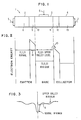
- Fig. 1 represents a transistor structure according to the invention;
- Fig. 2 represents the electron energy levels in the various regions of the transistor structure of Fig. 1; and
- Fig. 3 is an energy level diagram illustrating the upper valley condition in the base of the transistor structure of Fig. 1.
- Referring to Fig. 1, a three-terminal semiconductor structure is illustrated wherein a monocrystalline semiconductor body 1 is provided with an
emitter region 2, abase region 3, and a collector region 4, the emitter, base and collector regions having ohmic contacts 5, 6 and 7 respectively. - The
emitter region 2 is made up of two parts, 8 and 9,part 8 being the part to which the ohmic contact 5 is made and part 9 being a barrier portion which extends to a higher energy level than theexternal portion 8 and has a thickness small enough for quantum mechanical tunnelling of charge carriers across the emitter base junction 10 (represented by asawtooth arrow 14 in Fig. 2). The emitter and base have different conduction band minima. This is achieved in this structure by theportions 8 and 9 being made of different semiconductor materials. The injected carriers are of the type that have the higher mobility. In most materials these are usually electrons and the description will be set forth in terms of electrons although in the light of the principles set forth one skilled in the art will readily be able to select the appropriate higher mobility carrier. Theemitter 2 andbase 3 regions are selected such that there are normal electron states labelled (1,1,1) in theregion 8 of theemitter 2 that have the same energy level as upper valley states in thebase region 3. - The
base region 3 is of a different semiconductor material epitaxial with the material of the emitter region. The material of thebase 3 has a different lower energy level than the materials of the emitter and has a thickness sufficiently small for electron transport across the base to collector junction 11 to occur before the electrons scatter to this lower level. Thebase 3 has an excited upper valley state with electrons having energy labelled (1,1,1). - The collector region 4 is made up of two
sections Section 12 serves as the collector barrier. It is epitaxial with thebase 3 material. Thecollector barrier 12 extends to a higher energy level than the level of normal electrons in thebase region 3, the level being close to the upper valley level in the base.Section 12 prevents the normal electrons in the lower minimum energy level from flowing into the collector. Carriers that traverse the collector barrier (represented by arrow 15) enter thesection 13 and give up energy until they reach a lower energy level. - The barrier height and the barrier width in the emitter or carrier injecting region 9 is selected such that the dominant current injection mechanism is that of quantum mechanical tunnelling. Referring to Fig. 3 there is shown a schematic energy level diagram illustrating the fact that carriers in certain materials exhibit a normal energy minimum and an upper valley minimum at a higher energy level.
- The
emitter 2 andbase 3 semiconductor materials are selected such that normal electrons with for example (1,1,1) momentum from theemitter 2 are injected into an upper valley excited state of thebase 3 of the same, for example (1,1,1), momentum. - The predominant current conduction mechanism through the
base 3 is that of upper valley carrier transport without relaxation to the normal minimum level. The material of thebase 3 is selected so that there is an upper valley level labelled for example (1,1,1) and a lower energy minimum labelled for example (0,0,0). These conditions permit transit to occur across the base with a much reduced probability of energy loss as compared to the case where the carriers relax within the same minimum. This occurs because of a much lower rate of scattering outside the (1,1,1) valleys. - in accordance with the invention, a series of materials are structurally combined such that injected carriers enter an upper valley of the base so that the carriers will traverse the base to the collector with a much lover probability that they will lose energy in the process.
- In selecting the semiconductor materials for the emitter and base, it is necessary that the base material have an upper conduction minimum or valley that is substantially above the lowest conduction band states of the material and that the emitter material have normal states of the same type as the excited states in the base region. Some materials may have more than one minimum. Electrons in the upper valley will remain in quasithermal equilibrium with the lattice of the crystal and will only lose a significant amount of energy if they scatter by a relatively less probable process to states that are in the lowest conduction minimum. This is shown in Fig. 3 by the arrow labelled A. In operation of the device, normal electrons in the emitter, for example (1,1,1) electrons, are injected into a (1,1,1) upper valley base material so that transport can take place with reduced probability of energy loss. The device operates with very high speed and provides switching in the range of 10-12 seconds.
- In the structure of the device the various layers will be epitaxial with the same lattice periodicity. Under these conditions, it should be expected that the transverse momentum of the electrons will be conserved in any tunnelling process between the
emitter 2 and thebase 3. Tunnelling processes that do not conserve momentum have a low probability of occurring. - It has been found that these conditions are sensitive to crystallographic directions. crystallographic directions are indicated by Miller indices for intercepts with crystalline axes, as for example [1,0,0]. Where the crystallographic directions of the individual layers are properly arranged, the electrons will only tunnel efficiently into the higher upper valley states but not into the lower states since these states have a different transverse momentum.
- Referring to Figs. 1 and 2 together, a five-layer structure is provided. The
emitter region 2 is made of epitaxial layers of semiconductor material, thefirst region 8 of which has energies for normal electrons that correspond to upper valley energies in the base. These valleys have been labelled for example (1,1,1). A barrier region 9 is provided. The barrier 9 is of a higher energy level than the (1,1,1) level and is sufficiently thin for quantummechanical tunnelling 14 of the electrons. - The
base region 3 is made of a semiconductor material that is epitaxial with the region 9 and has an upper valley level corresponding to the emitter example (1,1,1) minima with a (0,0,0) minimum that is lower. Theregion 3 is sufficiently narrow that an injected carrier will remain in the upper valleys in quasithermal equilibrium with the lattice until it reaches the collector region. - The
collector barrier region 12 is again epitaxial with thebase 3. Theregion 12 has a barrier that is lower than the emitter barrier and at most only slightly higher than the (1,1,1) level. The remaining region of the collector has a normal level lower than the base region. - To provide a starting place for one skilled in the art to practice the invention, the interrelated semiconductor conditions are set forth in three examples in Table 1.
- Referring to the first example of Table 1 and the diagrams of Figs. 1 and 2, the first two
layers 8 and 9 function as theemitter 2 and consist of asemiconductor layer 8 with normal electrons at the (111) level. The ternary material GaAlAs with significant Al, for example Ga0.5Al0.5As, that is crystallographically oriented in the [100] direction will satisfy these criteria. The barrier region 9 is thin, about 25 Angstroms wide. A material such as AlAs will satisfy the required conditions and under these conditions electron majority carriers will tunnel through from the normal (1,1,1) states of the Ga0.5Al0.5As into the (1,1,1) upper valley states of thebase region 3. A material that satisfies the requirements to have a (1,1,1) upper valley for the base is GaAs. Tunnelling into the (000) minimum in the GaAs will be relatively improbable because of the transverse momentum conservation between the electrons in the layers when all layers are grown in the [100] crystallographic direction. - The width of the
base region 3 should be such that carrier transport is efficient. A width of the order of 250 Angstroms is adequate for this purpose.
- The collector region 4 is made up of a
barrier region 12 and anexternal region 13. Thebarrier region 12 is thin and has at most a small barrier over the upper valley (1,1,1) level. An approximately 50 Angstrom layer of Ga0.75Al0.25As is satisfactory. This provides a barrier of about 0.3 volts to the flow of electrons from the minimum (0,0,0) in thebase 3, while acting as only a very small barrier, approximately 0.04 volts to electrons at the (1,1,1) upper valley level traveling through the GaAs base. The collector has alayer 13 with a lower normal electron level and may be GaAs. - The
base region 3 will be moderately heavily doped to provide a. fairly highly conductive base for the chosen base layer thickness of 250 Angstroms so that the base sheet resistance is roughly 500 ohms centimeters. For such a structure as Example 1 of Table 1, the base transit time is approximately 0.3 x 10⁻¹² seconds. Thus, it may be seen that the parameters relating to speed are 20 to 50 times faster than the current silicon bipolar technology. - The time required for electrons to scatter to the (0,0,0) minimum will be approximately 3 x 10-11 seconds and a gain of approximately 100 is realized.
- Referring to Example 2 of Table 1, the material Ge is employed for the
outer emitter region 8. - Referring next to Example 3 of Table 1, this device has advantages because the transport across the base may occur, using as the upper valley the upper (0,0,0) conduction minimum of the material Ge. Because of the small effective mass (approximately 0.04 m, where m is the mass of the electron) of free electrons in this valley and the absence of polar scattering in Ge, an extremely fast device will be achieved. For this choice of materials, the transport across the base may be ballistic although this is not an essential requirement.
- Some temperature sensitivity of the device performance is to be expected because of the lower value of energy difference in Ge between the (0,0,0) and the (1,1,1) states. It is necessary that all of the materials be epitaxially compatible with each other. They may be deposited in layers using the well established liquid phase epitaxy and molecular beam epitaxy techniques.
- Since electrons seem usually to have higher mobility and most devices are constructed using electrons as minority carriers, the discussion and illustrations have been directed to electron flow. However, it should be clear to one skilled in the art that the appropriate substitutions could readily be made in the light of the principles set forth for conversion to the use of holes as minority carriers.
- In order to provide a perspective for one skilled in the art to practise this invention, a comparison is provided in Table 2 of the types of carriers and energy loss mechanisms involved in the upper valley device of this invention and the two prior art devices, the conventional bipolar device and the ballistic or hot electron device. The energy loss mechanism is that mechanism that so changes the energy or state of a minority carrier going through the base that it no longer is able to pass into the collector as part of the collector current.

- What has been described is a structure for the transport of carriers injected by tunnelling wherein materials are assembled with appropriate crystallographic orientations so that carriers from a normal energy level in the emitter region tunnel into an upper valley of the same energy level in the base so that they may travel rapidly to the collector with a small probability of loss.
Claims (7)
Applications Claiming Priority (2)
| Application Number | Priority Date | Filing Date | Title |
|---|---|---|---|
| US06/272,874 US4396931A (en) | 1981-06-12 | 1981-06-12 | Tunnel emitter upper valley transistor |
| US272874 | 1999-03-19 |
Publications (2)
| Publication Number | Publication Date |
|---|---|
| EP0067276A1 true EP0067276A1 (en) | 1982-12-22 |
| EP0067276B1 EP0067276B1 (en) | 1985-03-13 |
Family
ID=23041659
Family Applications (1)
| Application Number | Title | Priority Date | Filing Date |
|---|---|---|---|
| EP82102226A Expired EP0067276B1 (en) | 1981-06-12 | 1982-03-18 | Transistor with tunnel emitter and upper energy valley base |
Country Status (5)
| Country | Link |
|---|---|
| US (1) | US4396931A (en) |
| EP (1) | EP0067276B1 (en) |
| JP (1) | JPS57208171A (en) |
| CA (1) | CA1165464A (en) |
| DE (1) | DE3262514D1 (en) |
Cited By (7)
| Publication number | Priority date | Publication date | Assignee | Title |
|---|---|---|---|---|
| EP0084393A2 (en) * | 1982-01-18 | 1983-07-27 | Laboratoires D'electronique Et De Physique Appliquee L.E.P. | Semiconductor device of the heterojunction transistor type |
| EP0159273A2 (en) * | 1984-04-17 | 1985-10-23 | Fujitsu Limited | Semiconductor device |
| WO1986004184A1 (en) * | 1985-01-09 | 1986-07-17 | American Telephone & Telegraph Company | Hot electron unipolar transistor |
| EP0216155A2 (en) * | 1985-08-23 | 1987-04-01 | Texas Instruments Incorporated | Three-terminal tunnelling device |
| EP0299686A2 (en) * | 1987-07-17 | 1989-01-18 | AT&T Corp. | Hot electron transistor |
| US4959696A (en) * | 1985-08-23 | 1990-09-25 | Texas Instruments Incorporated | Three terminal tunneling device and method |
| US5059545A (en) * | 1985-08-23 | 1991-10-22 | Texas Instruments Incorporated | Three terminal tunneling device and method |
Families Citing this family (14)
| Publication number | Priority date | Publication date | Assignee | Title |
|---|---|---|---|---|
| EP0068064A1 (en) * | 1981-06-30 | 1983-01-05 | International Business Machines Corporation | Semiconductor circuit including a resonant quantum mechanical tunnelling triode device |
| US4794440A (en) * | 1983-05-25 | 1988-12-27 | American Telephone And Telegraph Company, At&T Bell Laboratories | Heterojunction bipolar transistor |
| DE3334167A1 (en) * | 1983-09-21 | 1985-04-04 | Siemens AG, 1000 Berlin und 8000 München | SEMICONDUCTOR DIODE |
| US4672413A (en) * | 1984-04-16 | 1987-06-09 | Trw Inc. | Barrier emitter transistor |
| JPS61248561A (en) * | 1985-04-25 | 1986-11-05 | インタ−ナショナル・ビジネス・マシ−ンズ・コ−ポレ−ション | Semiconductor structural body |
| US4665412A (en) * | 1985-06-19 | 1987-05-12 | Ga Technologies Inc. | Coupled heterostructure superlattice devices |
| US4716445A (en) * | 1986-01-17 | 1987-12-29 | Nec Corporation | Heterojunction bipolar transistor having a base region of germanium |
| JPS62211948A (en) * | 1986-03-13 | 1987-09-17 | Fujitsu Ltd | Hetero junction semiconductor device |
| JPH01503344A (en) * | 1986-05-29 | 1989-11-09 | リージェンツ オブ ザ ユニバーシティ オブ ミネソタ | Tunnel emitter bipolar transistor |
| JPS63153867A (en) * | 1986-08-04 | 1988-06-27 | Fujitsu Ltd | Resonance tunneling semiconductor device |
| FI81682C (en) * | 1986-12-29 | 1990-11-12 | Elecid Ab Oy | Cable break detector |
| JPS63310167A (en) * | 1987-06-12 | 1988-12-19 | Agency Of Ind Science & Technol | Semiconductor device |
| US5258624A (en) * | 1988-05-27 | 1993-11-02 | U.S. Philips Corp. | Transferred electron effect device |
| US10991847B2 (en) * | 2019-01-18 | 2021-04-27 | Alliance For Sustainable Energy, Llc | Semiconducting devices containing quantum wells |
Citations (1)
| Publication number | Priority date | Publication date | Assignee | Title |
|---|---|---|---|---|
| FR2394174A1 (en) * | 1977-06-09 | 1979-01-05 | Ibm | HIGH-SPEED HETEROJUNCTIONS SEMICONDUCTOR TYPE TRANSISTOR DEVICE |
Family Cites Families (6)
| Publication number | Priority date | Publication date | Assignee | Title |
|---|---|---|---|---|
| US3467896A (en) * | 1966-03-28 | 1969-09-16 | Varian Associates | Heterojunctions and domain control in bulk negative conductivity semiconductors |
| GB1354511A (en) * | 1970-04-22 | 1974-06-05 | Secr Defence | Semiconductor devices |
| US3927385A (en) * | 1972-08-03 | 1975-12-16 | Massachusetts Inst Technology | Light emitting diode |
| RO68248A2 (en) * | 1974-11-08 | 1981-03-30 | Institutul De Fizica,Ro | SEMICONDUCTOR DEVICE WITH MEMORY EFFECT |
| US4353081A (en) * | 1980-01-29 | 1982-10-05 | Bell Telephone Laboratories, Incorporated | Graded bandgap rectifying semiconductor devices |
| US4286275A (en) * | 1980-02-04 | 1981-08-25 | International Business Machines Corporation | Semiconductor device |
-
1981
- 1981-06-12 US US06/272,874 patent/US4396931A/en not_active Expired - Lifetime
-
1982
- 1982-03-18 EP EP82102226A patent/EP0067276B1/en not_active Expired
- 1982-03-18 DE DE8282102226T patent/DE3262514D1/en not_active Expired
- 1982-03-18 JP JP57041816A patent/JPS57208171A/en active Granted
- 1982-03-23 CA CA000399135A patent/CA1165464A/en not_active Expired
Patent Citations (1)
| Publication number | Priority date | Publication date | Assignee | Title |
|---|---|---|---|---|
| FR2394174A1 (en) * | 1977-06-09 | 1979-01-05 | Ibm | HIGH-SPEED HETEROJUNCTIONS SEMICONDUCTOR TYPE TRANSISTOR DEVICE |
Cited By (11)
| Publication number | Priority date | Publication date | Assignee | Title |
|---|---|---|---|---|
| EP0084393A2 (en) * | 1982-01-18 | 1983-07-27 | Laboratoires D'electronique Et De Physique Appliquee L.E.P. | Semiconductor device of the heterojunction transistor type |
| EP0084393A3 (en) * | 1982-01-18 | 1983-08-10 | Laboratoires D'electronique Et De Physique Appliquee L.E.P. | Semiconductor device of the heterojunction transistor type |
| EP0159273A2 (en) * | 1984-04-17 | 1985-10-23 | Fujitsu Limited | Semiconductor device |
| EP0159273A3 (en) * | 1984-04-17 | 1986-07-23 | Fujitsu Limited | Semiconductor device |
| WO1986004184A1 (en) * | 1985-01-09 | 1986-07-17 | American Telephone & Telegraph Company | Hot electron unipolar transistor |
| EP0216155A2 (en) * | 1985-08-23 | 1987-04-01 | Texas Instruments Incorporated | Three-terminal tunnelling device |
| EP0216155A3 (en) * | 1985-08-23 | 1989-03-15 | Texas Instruments Incorporated | Three-terminal tunnelling device |
| US4959696A (en) * | 1985-08-23 | 1990-09-25 | Texas Instruments Incorporated | Three terminal tunneling device and method |
| US5059545A (en) * | 1985-08-23 | 1991-10-22 | Texas Instruments Incorporated | Three terminal tunneling device and method |
| EP0299686A2 (en) * | 1987-07-17 | 1989-01-18 | AT&T Corp. | Hot electron transistor |
| EP0299686A3 (en) * | 1987-07-17 | 1990-01-24 | American Telephone And Telegraph Company | Hot electron transistor |
Also Published As
| Publication number | Publication date |
|---|---|
| JPH0241181B2 (en) | 1990-09-14 |
| EP0067276B1 (en) | 1985-03-13 |
| DE3262514D1 (en) | 1985-04-18 |
| US4396931A (en) | 1983-08-02 |
| CA1165464A (en) | 1984-04-10 |
| JPS57208171A (en) | 1982-12-21 |
Similar Documents
| Publication | Publication Date | Title |
|---|---|---|
| EP0067276B1 (en) | Transistor with tunnel emitter and upper energy valley base | |
| EP0133342B1 (en) | A superlattice type semiconductor structure having a high carrier density | |
| EP0033876B1 (en) | Three-terminal semiconductor device | |
| US4847666A (en) | Hot electron transistors | |
| US4878095A (en) | Semiconductor device in particular a hot electron transistor | |
| KR910004315B1 (en) | Hot electron unipolar transistor | |
| EP0068064A1 (en) | Semiconductor circuit including a resonant quantum mechanical tunnelling triode device | |
| US4716445A (en) | Heterojunction bipolar transistor having a base region of germanium | |
| US4825264A (en) | Resonant tunneling semiconductor device | |
| KR920006434B1 (en) | Resonant tunelling barrier structure device | |
| US5049955A (en) | Semiconductor ballistic electron velocity control structure | |
| US5391897A (en) | Status induction semiconductor device | |
| US4532533A (en) | Ballistic conduction semiconductor device | |
| US5497012A (en) | Unipolar band minima devices | |
| EP0229672B1 (en) | A heterojunction bipolar transistor having a base region of germanium | |
| JP2505805B2 (en) | Hot carrier transistor | |
| EP0247667B1 (en) | Hot charge-carrier transistors | |
| EP0251352B1 (en) | Hot charge-carrier transistors | |
| US5436469A (en) | Band minima transistor | |
| JPS6381854A (en) | Semiconductor device | |
| JPS6246566A (en) | Semiconductor device | |
| JPH06163569A (en) | Heterojunction bipolar transistor | |
| JPS60262466A (en) | Junction type transistor | |
| JPH0573352B2 (en) |
Legal Events
| Date | Code | Title | Description |
|---|---|---|---|
| PUAI | Public reference made under article 153(3) epc to a published international application that has entered the european phase |
Free format text: ORIGINAL CODE: 0009012 |
|
| AK | Designated contracting states |
Designated state(s): DE FR GB IT |
|
| 17P | Request for examination filed |
Effective date: 19830420 |
|
| GRAA | (expected) grant |
Free format text: ORIGINAL CODE: 0009210 |
|
| AK | Designated contracting states |
Designated state(s): DE FR GB IT |
|
| PG25 | Lapsed in a contracting state [announced via postgrant information from national office to epo] |
Ref country code: IT Free format text: LAPSE BECAUSE OF FAILURE TO SUBMIT A TRANSLATION OF THE DESCRIPTION OR TO PAY THE FEE WITHIN THE PRESCRIBED TIME-LIMIT;WARNING: LAPSES OF ITALIAN PATENTS WITH EFFECTIVE DATE BEFORE 2007 MAY HAVE OCCURRED AT ANY TIME BEFORE 2007. THE CORRECT EFFECTIVE DATE MAY BE DIFFERENT FROM THE ONE RECORDED. Effective date: 19850313 |
|
| REF | Corresponds to: |
Ref document number: 3262514 Country of ref document: DE Date of ref document: 19850418 |
|
| ET | Fr: translation filed | ||
| PLBE | No opposition filed within time limit |
Free format text: ORIGINAL CODE: 0009261 |
|
| STAA | Information on the status of an ep patent application or granted ep patent |
Free format text: STATUS: NO OPPOSITION FILED WITHIN TIME LIMIT |
|
| 26N | No opposition filed | ||
| PGFP | Annual fee paid to national office [announced via postgrant information from national office to epo] |
Ref country code: DE Payment date: 19920321 Year of fee payment: 11 |
|
| ITTA | It: last paid annual fee | ||
| PGFP | Annual fee paid to national office [announced via postgrant information from national office to epo] |
Ref country code: GB Payment date: 19930216 Year of fee payment: 12 |
|
| PGFP | Annual fee paid to national office [announced via postgrant information from national office to epo] |
Ref country code: FR Payment date: 19930226 Year of fee payment: 12 |
|
| PG25 | Lapsed in a contracting state [announced via postgrant information from national office to epo] |
Ref country code: DE Effective date: 19931201 |
|
| PG25 | Lapsed in a contracting state [announced via postgrant information from national office to epo] |
Ref country code: GB Effective date: 19940318 |
|
| GBPC | Gb: european patent ceased through non-payment of renewal fee |
Effective date: 19940318 |
|
| PG25 | Lapsed in a contracting state [announced via postgrant information from national office to epo] |
Ref country code: FR Effective date: 19941130 |
|
| REG | Reference to a national code |
Ref country code: FR Ref legal event code: ST |