EP0064003B1 - Dispositif de traitement d'un échantillon par faisceau électronique impulsionnel - Google Patents
Dispositif de traitement d'un échantillon par faisceau électronique impulsionnel Download PDFInfo
- Publication number
- EP0064003B1 EP0064003B1 EP82400708A EP82400708A EP0064003B1 EP 0064003 B1 EP0064003 B1 EP 0064003B1 EP 82400708 A EP82400708 A EP 82400708A EP 82400708 A EP82400708 A EP 82400708A EP 0064003 B1 EP0064003 B1 EP 0064003B1
- Authority
- EP
- European Patent Office
- Prior art keywords
- condenser
- cathode
- capacity
- circuit
- anode
- Prior art date
- Legal status (The legal status is an assumption and is not a legal conclusion. Google has not performed a legal analysis and makes no representation as to the accuracy of the status listed.)
- Expired
Links
- 238000010894 electron beam technology Methods 0.000 title claims description 11
- 230000005684 electric field Effects 0.000 claims description 7
- 230000004936 stimulating effect Effects 0.000 claims 1
- 239000003990 capacitor Substances 0.000 description 37
- 239000000758 substrate Substances 0.000 description 7
- 230000001133 acceleration Effects 0.000 description 6
- 238000000605 extraction Methods 0.000 description 6
- 238000000137 annealing Methods 0.000 description 5
- 239000010410 layer Substances 0.000 description 3
- 239000002245 particle Substances 0.000 description 3
- OKTJSMMVPCPJKN-UHFFFAOYSA-N Carbon Chemical compound [C] OKTJSMMVPCPJKN-UHFFFAOYSA-N 0.000 description 2
- XUIMIQQOPSSXEZ-UHFFFAOYSA-N Silicon Chemical compound [Si] XUIMIQQOPSSXEZ-UHFFFAOYSA-N 0.000 description 2
- 230000000694 effects Effects 0.000 description 2
- 238000004880 explosion Methods 0.000 description 2
- 229910002804 graphite Inorganic materials 0.000 description 2
- 239000010439 graphite Substances 0.000 description 2
- 238000002513 implantation Methods 0.000 description 2
- 239000012535 impurity Substances 0.000 description 2
- 238000005468 ion implantation Methods 0.000 description 2
- 150000002500 ions Chemical class 0.000 description 2
- 238000000034 method Methods 0.000 description 2
- 239000011806 microball Substances 0.000 description 2
- 239000004065 semiconductor Substances 0.000 description 2
- 229910052710 silicon Inorganic materials 0.000 description 2
- 239000010703 silicon Substances 0.000 description 2
- 238000009834 vaporization Methods 0.000 description 2
- 230000008016 vaporization Effects 0.000 description 2
- 235000012431 wafers Nutrition 0.000 description 2
- 241001080024 Telles Species 0.000 description 1
- XAGFODPZIPBFFR-UHFFFAOYSA-N aluminium Chemical compound [Al] XAGFODPZIPBFFR-UHFFFAOYSA-N 0.000 description 1
- 229910052782 aluminium Inorganic materials 0.000 description 1
- 229910052787 antimony Inorganic materials 0.000 description 1
- WATWJIUSRGPENY-UHFFFAOYSA-N antimony atom Chemical compound [Sb] WATWJIUSRGPENY-UHFFFAOYSA-N 0.000 description 1
- 239000013078 crystal Substances 0.000 description 1
- 238000010586 diagram Methods 0.000 description 1
- 238000004146 energy storage Methods 0.000 description 1
- 239000002360 explosive Substances 0.000 description 1
- 239000007943 implant Substances 0.000 description 1
- 238000004519 manufacturing process Methods 0.000 description 1
- 239000000463 material Substances 0.000 description 1
- 230000035515 penetration Effects 0.000 description 1
- 230000001737 promoting effect Effects 0.000 description 1
- 239000002344 surface layer Substances 0.000 description 1
Images
Classifications
-
- H—ELECTRICITY
- H01—ELECTRIC ELEMENTS
- H01J—ELECTRIC DISCHARGE TUBES OR DISCHARGE LAMPS
- H01J37/00—Discharge tubes with provision for introducing objects or material to be exposed to the discharge, e.g. for the purpose of examination or processing thereof
- H01J37/02—Details
- H01J37/24—Circuit arrangements not adapted to a particular application of the tube and not otherwise provided for
-
- H—ELECTRICITY
- H01—ELECTRIC ELEMENTS
- H01J—ELECTRIC DISCHARGE TUBES OR DISCHARGE LAMPS
- H01J37/00—Discharge tubes with provision for introducing objects or material to be exposed to the discharge, e.g. for the purpose of examination or processing thereof
- H01J37/30—Electron-beam or ion-beam tubes for localised treatment of objects
- H01J37/305—Electron-beam or ion-beam tubes for localised treatment of objects for casting, melting, evaporating, or etching
Definitions
- the present invention relates to a device for processing a sample by pulsed electron beam. It applies in particular in the treatment of the surface layers of semiconductor materials.
- annealing word for making the implanted impurities electrically active and for rearranging the crystal lattice of the substrate which was disturbed during the bombardment.
- One of the most used techniques for carrying out this annealing step consists in bringing the implanted substrate to a high temperature (of the order of 900 to 1200 ° C.) for a certain time.
- Another technique more recent, consists in bringing to the surface, or at the level of the first implanted layers, a high energy density, for a very short time, so that very high temperatures are reached locally during this time. In certain cases, the temperatures reached make it possible to liquefy the first layers of the substrate, which makes it possible to cure the damage created during implantation.
- This supply of energy to the surface or to the first layers of the substrate can be carried out either by means of a light energy shot by means, for example of a laser or of a flash tube, or by using an intense beam of particles such as electrons.
- These light beams or particles can be wide or narrow beams, pulsed or not, and can scan the substrate so as to "anneal it at different points.
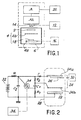
- the known devices for processing samples generally comprise a field and plasma emission diode known by the English expression of “field-plasma emission diode " Such a device has been shown in FIG. 1.
- This device therefore comprises a diode consisting of a cathode 2, generally made of graphite and provided with several grooves, and of an anode 4 consisting of an anode proper 4a and a grid 4b, these two elements 4a and 4b being brought to the same potential.
- This diode is generally placed in a vacuum enclosure 6.
- these devices include a high voltage generator 8, connected to a high voltage energy storage system 10 which may consist, for example, of a coaxial line or a capacitor, as well as a trigger system 12 pulse, connected to a switch 14, for example of the spark gap type known by the Anglo-Saxon expression "Spark gap switch”.
- a supply system 16 making it possible to present the samples to be treated 18 in the vacuum chamber 6, and systems 20 making it possible to measure the voltage and the current supplied by the generator 8 over time.
- the anode proper 4a serves as a support for the sample 18.
- the charging voltage of the capacitor 10 is applied by means of the spark gap 14 controlled by the pulse trigger system 12.
- the electric field created is intensified in the vicinity of the cathode by the presence of microprotubers, known by the English word “whiskers”, coming from the grooves (not shown) with which the cathode is provided.
- the electric power thus supplied is such that there is an explosion of these microprotuberances corresponding to an explosive vaporization and to an ionization of these.
- the plasma microballs thus formed in turn become a source of electrons promoting the rapid increase in current which itself promotes explosion. In a few nanoseconds, each of these plasma microballs extends enough for the cathode to be covered with a continuous plasma sheath. This sheath then sees, by the effect of relaxation, its thickness increasing until it reaches the grid of the anode, producing a short circuit of the diode known by the Anglo-Saxon expression of "diode-clo- safe •.
- the capacitor 10 charged by the generator 8 continues to discharge in the diode.
- the voltage applied between the anode and the cathode by the capacitor has made it possible, before the short circuit occurs, to extract and accelerate the electrons created so as to form an intense and pulsed electron beam which can, for example, be used for annealing. sample 18.
- the high voltage generator 8 via the capacitor 10, is used both for the creation of the plasma sheath which will be the source of the electrons and for the extraction and acceleration of the latter.
- Such devices make it possible to create electron beams whose energy is between 10 and 50 kiloelectronvolts (KeV), whose intensity is from 100 to a few thousand amperes per square centimeter and whose pulse duration is a few tens of nanoseconds to a few microseconds.
- KeV kiloelectronvolts
- the subject of the invention is precisely a device for processing a sample by pulsed electron beam making it possible to remedy these various drawbacks.
- the first circuit further comprises two identical resistors R 1 and R 2 , connected in series with the capacitor of capacitance C 1 , so that one of the terminals of the resistance R 1 is connected to the first armature of said capacitor and one of the terminals of the resistor R 2 is connected to the second armature of said capacitor, the spark gap being then connected on the one hand to the first armature of the capacitor of capacity Ci and, on the other hand, at the other terminal of the resistor R 2 , and it also includes the capacitor of capacity C 2 connected in parallel with the circuit R , Ci R 2 .
- the voltage applied between the cathode and the gate at the time of tripping of the spark gap is the sum voltages stored in capacitors of capacity Ci and C 2 , ie twice the voltage of the DC voltage generator.
- the device of the invention comprises inter alia a discharge tube comprising, as before, a cathode 22 provided with several grooves (not shown) and an anode 24 consisting of an anode proper 24a and of a grid 24b.
- This tube allows the production of intense and pulsed electron beams, capable of bombarding a sample 26 placed on the anode proper 24a which serves as its support.
- the use of the anode proper 24a as a sample support makes it possible to positively polarize the latter, which produces the penetration of the electrons in said sample and the removal of the ions also formed.
- the electrodes and the sample are placed in a vacuum enclosure such that 28. Means 30 are provided for bringing the sample 26 to be treated inside the enclosure 28.
- This device also comprises a direct high voltage generator 32 used to charge a capacitor Ci and a capacitor C 2 connected in parallel at a voltage V.
- the capacities C 1 and C 2 are such that the capacity C 2 is much greater than the capacity C 1 , that is to say that the capacity C 2 is 10 to 50 times greater than the capacity Ci.
- the capacitor of capacitance Ci is, moreover, connected in series with two identical resistors R 1 and R 2 , situated on either side of said capacitor.
- the resistor R 1 has one of its terminals connected to ground and the other terminal to one of the armatures of the capacitor of capacitance C 1
- the resistor R 2 has one of its terminals connected to the positive terminal of the high voltage generator 32 and the other terminal to the other armature of said capacitor.
- the assembly consisting of the two resistors R 1 and R 2 and of the capacitor of capacitance Ci can be connected in series with a resistor r and the capacitor of capacitance C 2 can be connected in series with a resistor R.
- the resistor R is much higher than the resistance r, as will be seen below in an exemplary embodiment.
- This device further comprises a spark gap 34 controlled by a pulse generator 36.
- This spark gap 34 is connected on the one hand to the positive terminal of the high voltage generator 32 via the resistor R and on the other hand, to the armature of the capacitor of capacity Ci connected to the resistor R 1 .
- the cathode 22 of the diode is connected to ground
- the grid 24b of the anode is connected to the terminal of the resistor R 2 which is connected to one of the armatures of the capacitor C 1 , and the anode proper 24a at the other terminal of the resistor R 2 via the resistor r.
- the circuit mainly comprising the capacitor of capacity C 1 , the capacitor of capacity C 2 and the spark gap 34, controlled by the pulse generator 36, constitutes a low power circuit (C 1 being less than C 2 ) making it possible to generate a plasma by creating a vaporization and an ionization in the vicinity of the cathode 22.
- the plasma is generated by the application across the grid-cathode space of the sum of the voltages stored in the capacitors of capacitors Ci and C 2 under the spark gap control 34.
- the circuit mainly comprising the capacitor of capacitance C 2 constitutes a high power circuit allowing the extraction and acceleration of the electrons produced by creating a large electric field between the anode proper 24a and the cathode 22.
- This circuit unlike those of the devices of the prior art, does not include a switch or spark gap, which makes it possible to avoid the problems posed by the abrupt closure of the high power circuit.
- the device of the invention has another advantage linked to the independence of the two functions, that is to say on the one hand the creation of the plasma and on the other hand, the extraction and acceleration of the electrons. This makes it possible to choose the extraction and acceleration voltage without this having any effect on the creation of the plasma, the power required being a function of the voltage supplied by the high-voltage generator 32 and the value of the capacitance C 2 of the corresponding capacitor.
- the operation of the device of the invention is identical to that of the prior art, except that the high power circuit does not include a switch.
- the use of two identical resistors R 1 and R 2 of very high impedance compared to those of the spark gap34 and of the capacitors Ci and C 2 makes it possible to obtain, when the pulse generator 36 triggers the spark gap34 causing the capacitor C 1 to discharge, a pulse between the grid 24b of the anode and the cathode 22 of the diode, the voltage of which is twice that supplied by the high-voltage generator 32. This is linked to the arrangement of the various components constituting the low power circuit.
- the high voltage generator makes it possible to charge the capacitors with capacities Ci and C 2 , respectively of 1 and 40 nanofarads, under a voltage of 30 kilovolts.
- the resistors R and r are respectively 30 Megohms (M ⁇ ) and 2 ⁇ and the resistors R 1 and R 2 , 300 M ⁇ .
- Samples processing tests were carried out on silicon wafers on a surface of approximately 2.5 cm in diameter by means of a diode whose cathode, of circular shape, had a diameter of 2.5 cm, whose distance between the cathode and the grid was 4 to 6 mm and whose distance between the grid and the anode proper was 0 to 3.5 cm.
- the energy brought in to anneal these wafers can be controlled, by means of the acceleration voltage, itself controlled, and by means of the distance between the anode proper and the grid. This distance also makes it possible to control the duration of the pulse.
- the energy supplied depends on the nature of the cathode. Indeed, the nature of the cathode makes it possible to control the nature of the plasma, therefore the speed of expansion, therefore the duration of the pulses and therefore of the energy supplied.
- sample processing described above relate to annealing of samples which have previously undergone ion implantation, but of course any other type of treatment can be envisaged.
- the trigger circuit capable of creating the plasma between cathode and gate, low power circuit, and the circuit for accelerating electrons to the anode, high power circuit can be independent, include separate high voltage generators and / or separate switches.
Landscapes
- Chemical & Material Sciences (AREA)
- Analytical Chemistry (AREA)
- Physics & Mathematics (AREA)
- Engineering & Computer Science (AREA)
- Plasma & Fusion (AREA)
- Plasma Technology (AREA)
- Electron Sources, Ion Sources (AREA)
Applications Claiming Priority (2)
| Application Number | Priority Date | Filing Date | Title |
|---|---|---|---|
| FR8108449 | 1981-04-28 | ||
| FR8108449A FR2504727A1 (fr) | 1981-04-28 | 1981-04-28 | Dispositif de traitement d'un echantillon par faisceau electronique impulsionnel |
Publications (2)
| Publication Number | Publication Date |
|---|---|
| EP0064003A1 EP0064003A1 (fr) | 1982-11-03 |
| EP0064003B1 true EP0064003B1 (fr) | 1985-02-20 |
Family
ID=9257870
Family Applications (1)
| Application Number | Title | Priority Date | Filing Date |
|---|---|---|---|
| EP82400708A Expired EP0064003B1 (fr) | 1981-04-28 | 1982-04-20 | Dispositif de traitement d'un échantillon par faisceau électronique impulsionnel |
Country Status (5)
| Country | Link |
|---|---|
| US (1) | US4527044A (enExample) |
| EP (1) | EP0064003B1 (enExample) |
| JP (1) | JPS57186325A (enExample) |
| DE (1) | DE3262385D1 (enExample) |
| FR (1) | FR2504727A1 (enExample) |
Families Citing this family (11)
| Publication number | Priority date | Publication date | Assignee | Title |
|---|---|---|---|---|
| JPS62222633A (ja) * | 1986-03-25 | 1987-09-30 | Sharp Corp | 半導体素子の製造方法 |
| US4894511A (en) * | 1986-08-26 | 1990-01-16 | Physical Sciences, Inc. | Source of high flux energetic atoms |
| US4731338A (en) * | 1986-10-09 | 1988-03-15 | Amoco Corporation | Method for selective intermixing of layered structures composed of thin solid films |
| US5003178A (en) * | 1988-11-14 | 1991-03-26 | Electron Vision Corporation | Large-area uniform electron source |
| US4904866A (en) * | 1988-11-17 | 1990-02-27 | Applied Electron Corporation | Wide area soft vacuum abnormal glow electron beam discharge hardening process |
| US5159170A (en) * | 1991-04-26 | 1992-10-27 | International Business Machines Corporation | Grid structure for reducing current density in focussed ion beam |
| US5449989A (en) * | 1992-07-31 | 1995-09-12 | Correa; Paulo N. | Energy conversion system |
| CA2126251A1 (en) | 1994-02-18 | 1995-08-19 | Ronald Sinclair Nohr | Process of enhanced chemical bonding by electron beam radiation |
| US5465030A (en) * | 1995-01-20 | 1995-11-07 | The United States Of America As Represented By The Secretary Of The Army | Trigger apparatus for spark gap dischargers |
| EP2035180A2 (en) * | 2006-06-20 | 2009-03-18 | CHISM, William, W., II | Method of direct coulomb explosion in laser ablation of semiconductor structures |
| FR2978600B1 (fr) | 2011-07-25 | 2014-02-07 | Soitec Silicon On Insulator | Procede et dispositif de fabrication de couche de materiau semi-conducteur |
Family Cites Families (6)
| Publication number | Priority date | Publication date | Assignee | Title |
|---|---|---|---|---|
| US3955091A (en) * | 1974-11-11 | 1976-05-04 | Accelerators, Inc. | Method and apparatus for extracting well-formed, high current ion beams from a plasma source |
| US3950187A (en) * | 1974-11-15 | 1976-04-13 | Simulation Physics, Inc. | Method and apparatus involving pulsed electron beam processing of semiconductor devices |
| US4082958A (en) * | 1975-11-28 | 1978-04-04 | Simulation Physics, Inc. | Apparatus involving pulsed electron beam processing of semiconductor devices |
| US4301391A (en) * | 1979-04-26 | 1981-11-17 | Hughes Aircraft Company | Dual discharge plasma device |
| US4335297A (en) * | 1979-09-18 | 1982-06-15 | Spire Corporation | Electron beam processor |
| US4344019A (en) * | 1980-11-10 | 1982-08-10 | The United States Of America As Represented By The United States Department Of Energy | Penning discharge ion source with self-cleaning aperture |
-
1981
- 1981-04-28 FR FR8108449A patent/FR2504727A1/fr active Granted
-
1982
- 1982-04-20 EP EP82400708A patent/EP0064003B1/fr not_active Expired
- 1982-04-20 DE DE8282400708T patent/DE3262385D1/de not_active Expired
- 1982-04-21 US US06/370,386 patent/US4527044A/en not_active Expired - Fee Related
- 1982-04-28 JP JP57072482A patent/JPS57186325A/ja active Pending
Also Published As
| Publication number | Publication date |
|---|---|
| DE3262385D1 (en) | 1985-03-28 |
| FR2504727B1 (enExample) | 1983-05-27 |
| JPS57186325A (en) | 1982-11-16 |
| EP0064003A1 (fr) | 1982-11-03 |
| US4527044A (en) | 1985-07-02 |
| FR2504727A1 (fr) | 1982-10-29 |
Similar Documents
| Publication | Publication Date | Title |
|---|---|---|
| EP0033685B1 (fr) | Procédé de dopage rapide de semiconducteurs | |
| EP0064003B1 (fr) | Dispositif de traitement d'un échantillon par faisceau électronique impulsionnel | |
| EP0112230B1 (fr) | Procédé et dispositif d'obtention de faisceaux de particules de densité spatialement modulée, application à la gravure et à l'implantation ioniques | |
| EP0645947B1 (fr) | Tube neutronique à confinement magnétique des électrons par aimants permanents et son procédé de fabrication | |
| FR2461350A1 (fr) | Dispositif semi-conducteur et son procede de fabrication ainsi que tube de prise de vues et dispositif de reproduction comportant un tel dispositif semi-conducteur | |
| FR2786359A1 (fr) | Tube a neutrons hermetique | |
| EP1236052B1 (fr) | Test electrique de l'interconnexion de conducteurs electriques sur un substrat | |
| EP0362947B1 (fr) | Tube neutronique scellé équipé d'une source d'ions multicellulaire à confinement magnétique | |
| EP0480518A1 (fr) | Source d'électrons présentant un dispositif de rétention de matières | |
| EP0362946A1 (fr) | Dispositif d'extraction et d'accélération des ions limitant la réaccélération des électrons secondaires dans un tube neutronique scellé à haut flux | |
| FR2491257A1 (fr) | Source d'electrons a grande densite a excitation par laser | |
| EP2718958B1 (fr) | Machine d'implantation ionique en mode immersion plasma pour procédé basse pression | |
| FR2529400A1 (fr) | Laser a gaz a excitation par decharge electrique transverse declenchee par photoionisation | |
| US4335314A (en) | Generator for pulsed electron beams | |
| WO2011151540A1 (fr) | Dispositif de mesure de dose pour l'implantation ionique en mode immersion plasma | |
| FR2472830A1 (fr) | Dispositif de commande de conduction electrique en mode a champs croises en plasma | |
| FR2984028A1 (fr) | Eclateur haute tension a amorcage par laser comportant une cathode en materiau refractaire poreux a charge photoemissive | |
| EP1763891B1 (fr) | Alimentation d'implanteur ionique prevue pour une limitation de l'effet de charge | |
| FR2762182A1 (fr) | Procede pour empecher l'accumulation d'une charge et dispositif d'implantation ionique | |
| EP0298817A1 (fr) | Procédé et dispositif de production d'électrons utilisant un couplage de champ et l'effet photoélectrique | |
| EP0362945A1 (fr) | Dispositif de perfectionnement de la source d'ions de type Penning dans un tube neutronique | |
| WO2024033273A1 (fr) | Dispositif de réduction de la charge électrique d'un véhicule spatial | |
| FR2635913A1 (fr) | Diode a emission de champ | |
| EP0351263A1 (fr) | Structure de source d'électrons et application aux tubes d'émission d'ondes électromagnétiques | |
| EP0497684A1 (fr) | Source d'alimentation électrique pour laser |
Legal Events
| Date | Code | Title | Description |
|---|---|---|---|
| PUAI | Public reference made under article 153(3) epc to a published international application that has entered the european phase |
Free format text: ORIGINAL CODE: 0009012 |
|
| AK | Designated contracting states |
Designated state(s): CH DE GB IT NL |
|
| 17P | Request for examination filed |
Effective date: 19830331 |
|
| ITF | It: translation for a ep patent filed | ||
| GRAA | (expected) grant |
Free format text: ORIGINAL CODE: 0009210 |
|
| AK | Designated contracting states |
Designated state(s): CH DE GB IT LI NL |
|
| REF | Corresponds to: |
Ref document number: 3262385 Country of ref document: DE Date of ref document: 19850328 |
|
| PLBE | No opposition filed within time limit |
Free format text: ORIGINAL CODE: 0009261 |
|
| STAA | Information on the status of an ep patent application or granted ep patent |
Free format text: STATUS: NO OPPOSITION FILED WITHIN TIME LIMIT |
|
| 26N | No opposition filed | ||
| PGFP | Annual fee paid to national office [announced via postgrant information from national office to epo] |
Ref country code: NL Payment date: 19870430 Year of fee payment: 6 |
|
| PG25 | Lapsed in a contracting state [announced via postgrant information from national office to epo] |
Ref country code: GB Effective date: 19890420 |
|
| PG25 | Lapsed in a contracting state [announced via postgrant information from national office to epo] |
Ref country code: LI Effective date: 19890430 Ref country code: CH Effective date: 19890430 |
|
| PG25 | Lapsed in a contracting state [announced via postgrant information from national office to epo] |
Ref country code: NL Effective date: 19891101 |
|
| NLV4 | Nl: lapsed or anulled due to non-payment of the annual fee | ||
| GBPC | Gb: european patent ceased through non-payment of renewal fee | ||
| REG | Reference to a national code |
Ref country code: CH Ref legal event code: PL |
|
| PG25 | Lapsed in a contracting state [announced via postgrant information from national office to epo] |
Ref country code: DE Effective date: 19900103 |