EP0064003B1 - Device for the pulsed electron beam processing of a specimen - Google Patents
Device for the pulsed electron beam processing of a specimen Download PDFInfo
- Publication number
- EP0064003B1 EP0064003B1 EP82400708A EP82400708A EP0064003B1 EP 0064003 B1 EP0064003 B1 EP 0064003B1 EP 82400708 A EP82400708 A EP 82400708A EP 82400708 A EP82400708 A EP 82400708A EP 0064003 B1 EP0064003 B1 EP 0064003B1
- Authority
- EP
- European Patent Office
- Prior art keywords
- condenser
- cathode
- capacity
- circuit
- anode
- Prior art date
- Legal status (The legal status is an assumption and is not a legal conclusion. Google has not performed a legal analysis and makes no representation as to the accuracy of the status listed.)
- Expired
Links
Images
Classifications
-
- H—ELECTRICITY
- H01—ELECTRIC ELEMENTS
- H01J—ELECTRIC DISCHARGE TUBES OR DISCHARGE LAMPS
- H01J37/00—Discharge tubes with provision for introducing objects or material to be exposed to the discharge, e.g. for the purpose of examination or processing thereof
- H01J37/02—Details
- H01J37/24—Circuit arrangements not adapted to a particular application of the tube and not otherwise provided for
-
- H—ELECTRICITY
- H01—ELECTRIC ELEMENTS
- H01J—ELECTRIC DISCHARGE TUBES OR DISCHARGE LAMPS
- H01J37/00—Discharge tubes with provision for introducing objects or material to be exposed to the discharge, e.g. for the purpose of examination or processing thereof
- H01J37/30—Electron-beam or ion-beam tubes for localised treatment of objects
- H01J37/305—Electron-beam or ion-beam tubes for localised treatment of objects for casting, melting, evaporating or etching
Definitions
- the present invention relates to a device for processing a sample by pulsed electron beam. It applies in particular in the treatment of the surface layers of semiconductor materials.
- annealing word for making the implanted impurities electrically active and for rearranging the crystal lattice of the substrate which was disturbed during the bombardment.
- One of the most used techniques for carrying out this annealing step consists in bringing the implanted substrate to a high temperature (of the order of 900 to 1200 ° C.) for a certain time.
- Another technique more recent, consists in bringing to the surface, or at the level of the first implanted layers, a high energy density, for a very short time, so that very high temperatures are reached locally during this time. In certain cases, the temperatures reached make it possible to liquefy the first layers of the substrate, which makes it possible to cure the damage created during implantation.
- This supply of energy to the surface or to the first layers of the substrate can be carried out either by means of a light energy shot by means, for example of a laser or of a flash tube, or by using an intense beam of particles such as electrons.
- These light beams or particles can be wide or narrow beams, pulsed or not, and can scan the substrate so as to "anneal it at different points.
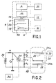
- the known devices for processing samples generally comprise a field and plasma emission diode known by the English expression of “field-plasma emission diode " Such a device has been shown in FIG. 1.
- This device therefore comprises a diode consisting of a cathode 2, generally made of graphite and provided with several grooves, and of an anode 4 consisting of an anode proper 4a and a grid 4b, these two elements 4a and 4b being brought to the same potential.
- This diode is generally placed in a vacuum enclosure 6.
- these devices include a high voltage generator 8, connected to a high voltage energy storage system 10 which may consist, for example, of a coaxial line or a capacitor, as well as a trigger system 12 pulse, connected to a switch 14, for example of the spark gap type known by the Anglo-Saxon expression "Spark gap switch”.
- a supply system 16 making it possible to present the samples to be treated 18 in the vacuum chamber 6, and systems 20 making it possible to measure the voltage and the current supplied by the generator 8 over time.
- the anode proper 4a serves as a support for the sample 18.
- the charging voltage of the capacitor 10 is applied by means of the spark gap 14 controlled by the pulse trigger system 12.
- the electric field created is intensified in the vicinity of the cathode by the presence of microprotubers, known by the English word “whiskers”, coming from the grooves (not shown) with which the cathode is provided.
- the electric power thus supplied is such that there is an explosion of these microprotuberances corresponding to an explosive vaporization and to an ionization of these.
- the plasma microballs thus formed in turn become a source of electrons promoting the rapid increase in current which itself promotes explosion. In a few nanoseconds, each of these plasma microballs extends enough for the cathode to be covered with a continuous plasma sheath. This sheath then sees, by the effect of relaxation, its thickness increasing until it reaches the grid of the anode, producing a short circuit of the diode known by the Anglo-Saxon expression of "diode-clo- safe •.
- the capacitor 10 charged by the generator 8 continues to discharge in the diode.
- the voltage applied between the anode and the cathode by the capacitor has made it possible, before the short circuit occurs, to extract and accelerate the electrons created so as to form an intense and pulsed electron beam which can, for example, be used for annealing. sample 18.
- the high voltage generator 8 via the capacitor 10, is used both for the creation of the plasma sheath which will be the source of the electrons and for the extraction and acceleration of the latter.
- Such devices make it possible to create electron beams whose energy is between 10 and 50 kiloelectronvolts (KeV), whose intensity is from 100 to a few thousand amperes per square centimeter and whose pulse duration is a few tens of nanoseconds to a few microseconds.
- KeV kiloelectronvolts
- the subject of the invention is precisely a device for processing a sample by pulsed electron beam making it possible to remedy these various drawbacks.
- the first circuit further comprises two identical resistors R 1 and R 2 , connected in series with the capacitor of capacitance C 1 , so that one of the terminals of the resistance R 1 is connected to the first armature of said capacitor and one of the terminals of the resistor R 2 is connected to the second armature of said capacitor, the spark gap being then connected on the one hand to the first armature of the capacitor of capacity Ci and, on the other hand, at the other terminal of the resistor R 2 , and it also includes the capacitor of capacity C 2 connected in parallel with the circuit R , Ci R 2 .
- the voltage applied between the cathode and the gate at the time of tripping of the spark gap is the sum voltages stored in capacitors of capacity Ci and C 2 , ie twice the voltage of the DC voltage generator.
- the device of the invention comprises inter alia a discharge tube comprising, as before, a cathode 22 provided with several grooves (not shown) and an anode 24 consisting of an anode proper 24a and of a grid 24b.
- This tube allows the production of intense and pulsed electron beams, capable of bombarding a sample 26 placed on the anode proper 24a which serves as its support.
- the use of the anode proper 24a as a sample support makes it possible to positively polarize the latter, which produces the penetration of the electrons in said sample and the removal of the ions also formed.
- the electrodes and the sample are placed in a vacuum enclosure such that 28. Means 30 are provided for bringing the sample 26 to be treated inside the enclosure 28.
- This device also comprises a direct high voltage generator 32 used to charge a capacitor Ci and a capacitor C 2 connected in parallel at a voltage V.
- the capacities C 1 and C 2 are such that the capacity C 2 is much greater than the capacity C 1 , that is to say that the capacity C 2 is 10 to 50 times greater than the capacity Ci.
- the capacitor of capacitance Ci is, moreover, connected in series with two identical resistors R 1 and R 2 , situated on either side of said capacitor.
- the resistor R 1 has one of its terminals connected to ground and the other terminal to one of the armatures of the capacitor of capacitance C 1
- the resistor R 2 has one of its terminals connected to the positive terminal of the high voltage generator 32 and the other terminal to the other armature of said capacitor.
- the assembly consisting of the two resistors R 1 and R 2 and of the capacitor of capacitance Ci can be connected in series with a resistor r and the capacitor of capacitance C 2 can be connected in series with a resistor R.
- the resistor R is much higher than the resistance r, as will be seen below in an exemplary embodiment.
- This device further comprises a spark gap 34 controlled by a pulse generator 36.
- This spark gap 34 is connected on the one hand to the positive terminal of the high voltage generator 32 via the resistor R and on the other hand, to the armature of the capacitor of capacity Ci connected to the resistor R 1 .
- the cathode 22 of the diode is connected to ground
- the grid 24b of the anode is connected to the terminal of the resistor R 2 which is connected to one of the armatures of the capacitor C 1 , and the anode proper 24a at the other terminal of the resistor R 2 via the resistor r.
- the circuit mainly comprising the capacitor of capacity C 1 , the capacitor of capacity C 2 and the spark gap 34, controlled by the pulse generator 36, constitutes a low power circuit (C 1 being less than C 2 ) making it possible to generate a plasma by creating a vaporization and an ionization in the vicinity of the cathode 22.
- the plasma is generated by the application across the grid-cathode space of the sum of the voltages stored in the capacitors of capacitors Ci and C 2 under the spark gap control 34.
- the circuit mainly comprising the capacitor of capacitance C 2 constitutes a high power circuit allowing the extraction and acceleration of the electrons produced by creating a large electric field between the anode proper 24a and the cathode 22.
- This circuit unlike those of the devices of the prior art, does not include a switch or spark gap, which makes it possible to avoid the problems posed by the abrupt closure of the high power circuit.
- the device of the invention has another advantage linked to the independence of the two functions, that is to say on the one hand the creation of the plasma and on the other hand, the extraction and acceleration of the electrons. This makes it possible to choose the extraction and acceleration voltage without this having any effect on the creation of the plasma, the power required being a function of the voltage supplied by the high-voltage generator 32 and the value of the capacitance C 2 of the corresponding capacitor.
- the operation of the device of the invention is identical to that of the prior art, except that the high power circuit does not include a switch.
- the use of two identical resistors R 1 and R 2 of very high impedance compared to those of the spark gap34 and of the capacitors Ci and C 2 makes it possible to obtain, when the pulse generator 36 triggers the spark gap34 causing the capacitor C 1 to discharge, a pulse between the grid 24b of the anode and the cathode 22 of the diode, the voltage of which is twice that supplied by the high-voltage generator 32. This is linked to the arrangement of the various components constituting the low power circuit.
- the high voltage generator makes it possible to charge the capacitors with capacities Ci and C 2 , respectively of 1 and 40 nanofarads, under a voltage of 30 kilovolts.
- the resistors R and r are respectively 30 Megohms (M ⁇ ) and 2 ⁇ and the resistors R 1 and R 2 , 300 M ⁇ .
- Samples processing tests were carried out on silicon wafers on a surface of approximately 2.5 cm in diameter by means of a diode whose cathode, of circular shape, had a diameter of 2.5 cm, whose distance between the cathode and the grid was 4 to 6 mm and whose distance between the grid and the anode proper was 0 to 3.5 cm.
- the energy brought in to anneal these wafers can be controlled, by means of the acceleration voltage, itself controlled, and by means of the distance between the anode proper and the grid. This distance also makes it possible to control the duration of the pulse.
- the energy supplied depends on the nature of the cathode. Indeed, the nature of the cathode makes it possible to control the nature of the plasma, therefore the speed of expansion, therefore the duration of the pulses and therefore of the energy supplied.
- sample processing described above relate to annealing of samples which have previously undergone ion implantation, but of course any other type of treatment can be envisaged.
- the trigger circuit capable of creating the plasma between cathode and gate, low power circuit, and the circuit for accelerating electrons to the anode, high power circuit can be independent, include separate high voltage generators and / or separate switches.
Description
La présente invention a pour objet un dispositif de traitement d'un échantillon par faisceau électronique impulsionnel. Elle s'applique en particulier dans le traitement des couches superficielles des matériaux semiconducteurs.The present invention relates to a device for processing a sample by pulsed electron beam. It applies in particular in the treatment of the surface layers of semiconductor materials.
En effet, lorsque l'on implante par exemple dans un substrat semiconducteur, en effectuant un bombardement de celui-ci, des particules étrangères ou impuretés, on sait qu'il est nécessaire d'effectuer, après cette implantation, une étape connue sous le mot de recuit permettant de rendre électriquement actives les impuretés implantées et permettant de ré-arranger le réseau cristallin du substrat qui a été perturbé lors du bombardement.Indeed, when one implants for example in a semiconductor substrate, by bombarding it, foreign particles or impurities, it is known that it is necessary to carry out, after this implantation, a step known as annealing word for making the implanted impurities electrically active and for rearranging the crystal lattice of the substrate which was disturbed during the bombardment.
L'une des techniques les plus utilisées pour effectuer cette étape de recuit consiste à porter le substrat implanté à une température élevée (de l'ordre de 900 à 1 200 °C) pendant un certain temps.One of the most used techniques for carrying out this annealing step consists in bringing the implanted substrate to a high temperature (of the order of 900 to 1200 ° C.) for a certain time.
Une autre technique, plus récente, consiste à apporter à la surface, ou au niveau des premières couches implantées, une densité d'énergie élevée, pendant un temps très bref, de façon que de très hautes températures soient atteintes localement pendant ce temps. Dans certains cas, les températures atteintes permettent de liquéfier les premières couches du substrat, ce qui permet de guérir les dommages créés lors de l'implantation.Another technique, more recent, consists in bringing to the surface, or at the level of the first implanted layers, a high energy density, for a very short time, so that very high temperatures are reached locally during this time. In certain cases, the temperatures reached make it possible to liquefy the first layers of the substrate, which makes it possible to cure the damage created during implantation.
Etant donné que l'élévation de température est très localisée et de courte durée (inférieure à la milliseconde), le reste du substrat n'est pas affecté.Since the temperature rise is very localized and short-lived (less than a millisecond), the rest of the substrate is not affected.
Cet apport d'énergie à la surface ou sur les premières couches du substrat peut être réalisé, soit à l'aide d'un tir d'énergie lumineuse au moyen, par exemple d'un laser ou d'un tube éclair, soit à l'aide d'un faisceau intense de particules telles que des électrons. Ces faisceaux lumineux ou de particules peuvent être des faisceaux larges ou étroits, pulsés ou non, et peuvent balayer le substrat de façon à « recuire celui-ci en différents points.This supply of energy to the surface or to the first layers of the substrate can be carried out either by means of a light energy shot by means, for example of a laser or of a flash tube, or by using an intense beam of particles such as electrons. These light beams or particles can be wide or narrow beams, pulsed or not, and can scan the substrate so as to "anneal it at different points.
Les dispositifs connus pour traiter des échantillons, au moyen d'un faisceau d'électrons intenses et pulsés, comprennent, en général une diode d'émission de champ et de plasma connue sous l'expression anglo-saxonne de « field-plasma emission diode ». Un tel dispositif a été représenté sur la figure 1.The known devices for processing samples, by means of a beam of intense and pulsed electrons, generally comprise a field and plasma emission diode known by the English expression of “field-plasma emission diode " Such a device has been shown in FIG. 1.
Ce dispositif comprend donc, une diode constituée d'une cathode 2, généralement en graphite et munie de plusieurs sillons, et d'une anode 4 constituée d'une anode proprement dite 4a et d'une grille 4b, ces deux éléments 4a et 4b étant portés au même potentiel. Cette diode est généralement placée dans une enceinte à vide 6.This device therefore comprises a diode consisting of a
De plus, ces dispositifs comprennent un générateur de haute tension 8, relié à un système de stockage d'énergie sous haute tension 10 pouvant être constitué par exemple d'une ligne coaxiale ou d'un condensateur, ainsi qu'un système 12 de déclenchement d'impulsions, relié à un interrupteur 14, par exemple du type éclateur connu sous l'expression anglo-saxonne de « Spark gap switch ». Ces dispositifs comprennent, encore, un système d'amenée 16 permettant de présenter les échantillons à traiter 18 dans l'enceinte à vide 6, et des systèmes 20 permettant de mesurer la tension et le courant fournis par le générateur 8 au cours du temps. L'anode proprement dite 4a sert de support à l'échantillon 18.In addition, these devices include a high voltage generator 8, connected to a high voltage
De tels dispositifs ont été décrits, par exemple dans le brevet américain N° 3 950 187 et dans l'article du « Journal of Applied Physics •, vol. 50, n° 2 de février 1979 intitulé « Pulsed-electron- beam annealing of ion implantation damage ».Such devices have been described, for example in US patent 3,950,187 and in the article in the “Journal of Applied Physics •, vol. 50, n ° 2 of February 1979 entitled "Pulsed-electron-beam annealing of ion implantation damage".
Dans ces dispositifs, l'application d'une tension importante entre la grille 4b de l'anode et la cathode 2 au moyen par exemple d'un condensateur 10, chargé au préalable par le générateurs. permet de créer un champ électrique intense au voisinage de la cathode 2 de la diode. L'application de la tension de charge du condensateur 10 est assurée au moyen de l'éclateur 14 commandé par le système de déclenchement d'impulsions 12.In these devices, the application of a large voltage between the
Le champ électrique créé est intensifié au voisinage de la cathode par la présence de microprotubérances, connues sous le mot anglo- saxon de « whiskers •, provenant des sillons (non représentés) dont est munie la cathode. La puissance électrique ainsi fournie est telle que l'on assiste à une explosion de ces microprotubérances correspondant à une vaporisation explosive et à une ionisation de celles-ci. Les microboules de plasma ainsi formées deviennent à leur tour une source d'électrons favorisant l'augmentation rapide du courant qui favorise elle-même l'explosion. En quelques nanosecondes, chacune de ces microboules de plasma s'étend suffisamment pour que la cathode soit recouverte d'une gaine de plasma continue. Cette gaine voit alors, par effet de détente, son épaisseur augmenter jusqu'à ce qu'elle atteigne la grille de l'anode, produisant un court-circuit de la diode connue sous l'expression anglo-saxonne de « diode-clo- sure •.The electric field created is intensified in the vicinity of the cathode by the presence of microprotubers, known by the English word “whiskers”, coming from the grooves (not shown) with which the cathode is provided. The electric power thus supplied is such that there is an explosion of these microprotuberances corresponding to an explosive vaporization and to an ionization of these. The plasma microballs thus formed in turn become a source of electrons promoting the rapid increase in current which itself promotes explosion. In a few nanoseconds, each of these plasma microballs extends enough for the cathode to be covered with a continuous plasma sheath. This sheath then sees, by the effect of relaxation, its thickness increasing until it reaches the grid of the anode, producing a short circuit of the diode known by the Anglo-Saxon expression of "diode-clo- safe •.
Le condensateur 10 chargé par le générateur 8, continue à se décharger dans la diode. La tension appliquée entre anode et cathode par le condensateur a permis, avant que n'intervienne le court-circuit, d'extraire et d'accélérer les électrons créés de façon à former un faisceau électronique intense et pulsé qui peut par exemple servir à recuire l'échantillon 18.The
Le fait d'utiliser dans un tel dispositif une anode proprement dite 4a servant de support à l'échantillon 18, conduisant donc à polariser positivement ledit échantillon, permet aux électrons de pénétrer aisément dans celui-ci, tandis que les ions formés ne peuvent pas pénétrer dans l'échantillon, ceux-ci étant automatiquement repoussés. On obtient bien, ainsi, un faisceau d'électrons intense et pulsé.The fact of using in such a device an anode proper 4a serving as support for the
En conséquence, le générateur de haute tension 8, par l'intermédiaire du condensateur 10, sert à la fois à la création de la gaine de plasma qui sera la source des électrons et à l'extraction et accélération de ces derniers.Consequently, the high voltage generator 8, via the
De tels dispositifs permettent de créer des faisceaux d'électrons dont l'énergie est comprise entre 10 et 50 kiloélectronvolts (KeV), dont l'intensité est de 100 à quelques milliers d'ampères par centimètre carré et dont la durée des impulsions est de quelques dizaines de nanosecondes à quelques microsecondes.Such devices make it possible to create electron beams whose energy is between 10 and 50 kiloelectronvolts (KeV), whose intensity is from 100 to a few thousand amperes per square centimeter and whose pulse duration is a few tens of nanoseconds to a few microseconds.
Pour de plus amples détails sur le principe de fonctionnement de tels dispositifs, on peut se référer à l'article du « Journal of Applied Physics », vol. 45, N° 6 de juin 1974 intitulé « Plasma- induced field emission and the characteristics of high-current relativistic electron flow ».For further details on the operating principle of such devices, reference may be made to the article in the “Journal of Applied Physics”, vol. 45, No. 6 of June 1974 entitled "Plasma-induced field emission and the characteristics of high-current relativistic electron flow".
Ces dispositifs, de conception simple présentent un certain nombre d'inconvénients. Ces inconvénients sont, en particulier :
- - la nécessité d'engendrer brusquement une haute tension dans l'espace compris entre l'anode et la cathode dans des conditions telles que l'intensité doit être très importante, c'est-à-dire comprise entre 100 et 10000 ampères ;
- - les caractéristiques du faisceau d'électrons, c'est-à-dire son énergie et sa densité de courant ne peuvent pas être choisies indépendamment des conditions dans lesquelles est engendré le plasma. Par exemple, si l'on désire obtenir un faisceau d'électrons de faible énergie, c'est-à-dire de l'ordre de 20 KeV, il n'est pas évident que le champ électrique correspondant suffira à engendrer la gaine de plasma ;
- - l'utilisation d'un système à très forte puissance pour engendrer le plasma, alors que la création de celui-ci ne l'exige pas.
- - The need to suddenly generate a high voltage in the space between the anode and the cathode under conditions such that the intensity must be very high, that is to say between 100 and 10,000 amps;
- - the characteristics of the electron beam, that is to say its energy and its current density cannot be chosen independently of the conditions in which the plasma is generated. For example, if one wishes to obtain a low energy electron beam, that is to say of the order of 20 KeV, it is not obvious that the corresponding electric field will be sufficient to generate the sheath of plasma;
- - the use of a very high power system to generate the plasma, while the creation of it does not require it.
L'invention a justement pour objet un dispositif de traitement d'un échantillon par faisceau électronique impulsionnel permettant de remédier à ces différents inconvénients.The subject of the invention is precisely a device for processing a sample by pulsed electron beam making it possible to remedy these various drawbacks.
Le dispositif de l'invention, basé sur les mêmes principes que ceux décrits précédemment, permet de séparer les deux fonctions suivantes :
- - la création de la gaine de plasma, et
- - l'extraction et l'accélération des électrons créés, et utilise à cet effet les moyens mentionnés dans la revendication principale.
- - the creation of the plasma sheath, and
- - the extraction and acceleration of the electrons created, and uses for this purpose the means mentioned in the main claim.
De façon plus précise, l'invention a pour objet un dispositif de traitement d'un échantillon par faisceau électronique du genre de ceux décrits précédemment, mais dans lequel le tube à vide comporte trois électrodes indépendantes. Ce dispositif se caractérise en ce qu'il comprend, de plus :
- A) Un premier circuit pour créer de façon impulsionnelle un plasma à partir de la cathode du tube à vide, ce premier circuit comprenant :
- a) un condensateur de capacité C1 chargé au moyen du générateur de haute tension continue, ledit condensateur étant muni d'une première et d'une deuxième armatures,
- b) un éclateur permettant d'initier la décharge du condensateur de capacité Ci de façon à produire une impulsion de haute tension entre la cathode et la grille, ledit éclateur étant disposé en série avec ledit condensateur, et
- c) des moyens pour engendrer des impulsions commandant l'éclateur ; et
- B) Un deuxième circuit pour créer entre l'anode proprement dite et la cathode un champ électrique permettant d'accelérer et d'extraire les électrons produits de façon qu'ils viennent bombarder l'échantillon, ce deuxième circuit comprenant un condensateur de capacité C2 très supérieure à la capacité C1, ce condensateur de capacité C2 étant chargé au moyen du générateur de haute tension continue et pouvant se décharger par le tube à vide lui-même.
- A) A first circuit for impulsively creating a plasma from the cathode of the vacuum tube, this first circuit comprising:
- a) a capacitor of capacitance C 1 charged by means of the high-voltage direct generator, said capacitor being provided with first and second armatures,
- b) a spark gap making it possible to initiate the discharge of the capacitor of capacitance Ci so as to produce a high voltage pulse between the cathode and the grid, said spark gap being arranged in series with said capacitor, and
- c) means for generating pulses controlling the spark gap; and
- B) A second circuit to create between the anode proper and the cathode an electric field allowing to accelerate and extract the electrons produced so that they come to bombard the sample, this second circuit comprising a capacitor of capacity C 2 much greater than the capacity C 1 , this capacitor of capacity C 2 being charged by means of the high-voltage continuous generator and being able to discharge by the vacuum tube itself.
Selon un mode de réalisation préféré de l'invention, le premier circuit comprend, de plus, deux résistances identiques R1 et R2, reliées en série avec le condensateur de capacité C1, de façon que l'une des bornes de la résistance R1 soit reliée à la première armature dudit condensateur et que l'une des bornes de la résistance R2 soit reliée à la deuxième armature dudit condensateur, l'éclateur étant alors relié d'une part à la première armature du condensateur de capacité Ci et, d'autre part, à l'autre borne de la résistance R2, et il comprend également le condensateur de capacité C2 branché en parallèle avec le circuit R, Ci R 2.According to a preferred embodiment of the invention, the first circuit further comprises two identical resistors R 1 and R 2 , connected in series with the capacitor of capacitance C 1 , so that one of the terminals of the resistance R 1 is connected to the first armature of said capacitor and one of the terminals of the resistor R 2 is connected to the second armature of said capacitor, the spark gap being then connected on the one hand to the first armature of the capacitor of capacity Ci and, on the other hand, at the other terminal of the resistor R 2 , and it also includes the capacitor of capacity C 2 connected in parallel with the circuit R , Ci R 2 .
Dans ce mode de réalisation, et du fait de la valeur élevée des résistances R1 et R2 par rapport à l'impédance du reste du premier circuit, la tension appliquée entre cathode et grille au moment du déclenchement de l'éclateur est la somme des tensions stockées dans les condensateurs de capacité Ci et C2, soit deux fois la tension du générateur de tension continue.In this embodiment, and due to the high value of the resistors R 1 and R 2 relative to the impedance of the rest of the first circuit, the voltage applied between the cathode and the gate at the time of tripping of the spark gap is the sum voltages stored in capacitors of capacity Ci and C 2 , ie twice the voltage of the DC voltage generator.
D'autres caractéristiques et avantages de l'invention ressortiront mieux de la description qui va suivre, donnée à titre explicatif mais nullement limitatif, en référence aux figures annexées dans lesquelles :
- la figure 1, déjà décrite, représente schématiquement un dispositif de traitement d'échantillons de l'art antérieur, et
- la figure 2 représente schématiquement un dispositif de traitement d'échantillons conforme à l'invention.
- FIG. 1, already described, schematically represents a device for processing samples of the prior art, and
- FIG. 2 schematically represents a device for processing samples according to the invention.
Le dispositif de l'invention, schématisé sur la figure2, comprend entre autres un tube à décharge comportant, comme précédemment, une cathode 22 munie de plusieurs sillons (non représentés) et une anode 24 constituée d'une anode proprement dite 24a et d'une grille 24b. Ce tube permet la production de faisceaux d'électrons intenses et pulsés, susceptibles de bombarder un échantillon 26 placé sur l'anode proprement dite 24a qui lui sert de support. L'utilisation de l'anode proprement dite 24a en tant que support d'échantillon permet de polariser positivement celui-ci, ce qui produit la pénétration des électrons dans ledit échantillon et l'éloignement des ions aussi formés. Les électrodes et l'échantillon sont placés dans une enceinte à vide telle que 28. Des moyens 30 sont prévus pour amener à l'intérieur de l'enceinte 28 l'échantillon 26 à traiter.The device of the invention, shown diagrammatically in FIG. 2, comprises inter alia a discharge tube comprising, as before, a
Ce dispositif comprend, aussi, un générateur de haute tension continue 32 servant à charger sous une tension V un condensateur de capacité Ci et un condensateur de capacité C2 branchés en parallèle. Les capacités C1 et C2 sont telles que la capacité C2 est très supérieure à la capacité C1, c'est-à-dire que la capacité C2 est de 10 à 50 fois plus grande que la capacité Ci.This device also comprises a direct
Le condensateur de capacité Ci est, de plus, relié en série avec deux résistances identiques R1 et R2, situées de part et d'autre dudit condensateur. En effet, la résistance R1 a l'une de ses bornes connectée à la masse et l'autre borne à l'une des armatures du condensateur de capacité C1, tandis que la résistance R2 a l'une de ses bornes connectée à la borne positive du générateur haute tension 32 et l'autre borne à l'autre armature dudit condensateur.The capacitor of capacitance Ci is, moreover, connected in series with two identical resistors R 1 and R 2 , situated on either side of said capacitor. Indeed, the resistor R 1 has one of its terminals connected to ground and the other terminal to one of the armatures of the capacitor of capacitance C 1 , while the resistor R 2 has one of its terminals connected to the positive terminal of the
De plus, l'ensemble constitué des deux résistances R1 et R2 et du condensateur de capacité Ci peut être relié en série avec une résistance r et le condensateur de capacité C2 peut être relié en série avec une résistance R. La résistance R est très supérieure à la résistance r, comme on le verra ci-après dans un exemple de réalisation.In addition, the assembly consisting of the two resistors R 1 and R 2 and of the capacitor of capacitance Ci can be connected in series with a resistor r and the capacitor of capacitance C 2 can be connected in series with a resistor R. The resistor R is much higher than the resistance r, as will be seen below in an exemplary embodiment.
Ce dispositif comprend, encore, un éclateur 34 commandé par un générateur d'impulsions 36. Cet éclateur34 est relié d'une part à la borne positive du générateur haute tension 32 par l'intermédiaire de la résistance R et d'autre part, à l'armature du condensateur de capacité Ci reliée à la résistance R1.This device further comprises a
Dans le dispositif de l'invention, la cathode 22 de la diode est reliée à la masse, la grille 24b de l'anode est reliée à la borne de la résistance R2 qui est reliée à l'une des armatures du condensateur de capacité C1, et l'anode proprement dite 24a à l'autre borne de la résistance R2 par l'intermédiaire de la résistance r.In the device of the invention, the
Le circuit comprenant principalement le condensateur de capacité C1, le condensateur de capacité C2 et l'éclateur34, commandé par le générateur d'impulsions 36, constitue un circuit de faible puissance (C1 étant inférieur à C2) permettant d'engendrer un plasma en créant une vaporisation et une ionisation au voisinage de la cathode 22. Le plasma est engendré par l'application aux bornes de l'espace grille-cathode de la somme des tensions stockées dans les condensateurs de capacités Ci et C2 sous la commande de l'éclateur 34.The circuit mainly comprising the capacitor of capacity C 1 , the capacitor of capacity C 2 and the
Le circuit comprenant principalement le condensateur de capacité C2 constitue un circuit de forte puissance permettant l'extraction et l'accélération des électrons produits en créant un champ électrique important entre l'anode proprement dite 24a et la cathode 22. Ce circuit, contrairement à ceux des dispositifs de l'art antérieur, ne comprend pas d'interrupteur ou d'éclateur, ce qui permet d'éviter les problèmes posés par la fermeture brusque du circuit de forte puissance.The circuit mainly comprising the capacitor of capacitance C 2 constitutes a high power circuit allowing the extraction and acceleration of the electrons produced by creating a large electric field between the anode proper 24a and the
Le dispositif de l'invention présente un autre avantage lié à l'indépendance des deux fonctions, c'est-à-dire d'une part la création du plasma et d'autre part, l'extraction et l'accélération des électrons. Ceci permet de choisir la tension d'extraction et d'accélération sans que cela n'ait d'incidence sur la création du plasma, la puissance nécessaire étant fonction de la tension fournie par le générateur de haute tension 32 et de la valeur de la capacité C2 du condensateur correspondant.The device of the invention has another advantage linked to the independence of the two functions, that is to say on the one hand the creation of the plasma and on the other hand, the extraction and acceleration of the electrons. This makes it possible to choose the extraction and acceleration voltage without this having any effect on the creation of the plasma, the power required being a function of the voltage supplied by the high-
Comme on l'a déjà dit, le fonctionnement du dispositif de l'invention est identique à celui de l'art antérieur, si ce n'est le fait que le circuit de forte puissance ne comprend pas d'interrupteur. De plus, l'utilisation des deux résistances identiques R1 et R2 d'impédance très élevée par rapport à celles de l'éclateur34 et des capacités Ci et C2 permet d'obtenir, lorsque le générateur d'impulsions 36 déclenche l'éclateur34 provoquant la décharge du condensateur de capacité C1, une impulsion entre la grille 24b de l'anode et la cathode 22 de la diode, dont la tension est double de celle fournie par le générateur haute tension 32. Ceci est lié à l'agencement des différents composants constituant le circuit de faible puissance.As already mentioned, the operation of the device of the invention is identical to that of the prior art, except that the high power circuit does not include a switch. In addition, the use of two identical resistors R 1 and R 2 of very high impedance compared to those of the spark gap34 and of the capacitors Ci and C 2 makes it possible to obtain, when the
On va maintenant donner un exemple de réalisation ainsi que des exemples de traitement d'échantillons.We will now give an example of embodiment as well as examples of sample processing.
Le générateur haute tension permet de charger les condensateurs de capacités Ci et C2, respectivement de 1 et 40 nanofarads, sous une tension de 30 kilovolts. Les résistances R et r sont respectivement de 30 Mégohms (MΩ) et 2Ω et les résistances R1 et R2, de 300 MΩ.The high voltage generator makes it possible to charge the capacitors with capacities Ci and C 2 , respectively of 1 and 40 nanofarads, under a voltage of 30 kilovolts. The resistors R and r are respectively 30 Megohms (MΩ) and 2Ω and the resistors R 1 and R 2 , 300 MΩ.
Des essais de traitement d'échantillons ont été réalisés sur des plaquettes de silicium sur une surface d'environ 2,5 cm de diamètre au moyen d'une diode dont la cathode, de forme circulaire, présentait un diamètre de 2,5 cm, dont la distance entre la cathode et la grille était de 4 à 6 mm et dont celle entre la grille et l'anode proprement dite était de 0 à 3,5 cm.Samples processing tests were carried out on silicon wafers on a surface of approximately 2.5 cm in diameter by means of a diode whose cathode, of circular shape, had a diameter of 2.5 cm, whose distance between the cathode and the grid was 4 to 6 mm and whose distance between the grid and the anode proper was 0 to 3.5 cm.
L'énergie apportée pour recuire ces plaquettes peut être contrôlée, au moyen de la tension d'accélération, elle-même contrôlée, et au moyen de la distance entre l'anode proprement dite et la grille. Cette distance permet aussi de contrôler la durée de l'impulsion. De plus, l'énergie apportée dépend de la nature de la cathode. En effet, la nature de la cathode permet de contrôler la nature du plasma, donc la vitesse d'expansion, donc la durée des impulsions et donc de l'énergie apportée.The energy brought in to anneal these wafers can be controlled, by means of the acceleration voltage, itself controlled, and by means of the distance between the anode proper and the grid. This distance also makes it possible to control the duration of the pulse. In addition, the energy supplied depends on the nature of the cathode. Indeed, the nature of the cathode makes it possible to control the nature of the plasma, therefore the speed of expansion, therefore the duration of the pulses and therefore of the energy supplied.
Les essais ont été réalisés avec des cathodes de graphite, d'aluminium, d'antimoine et de silicium, correspondant respectivement à une vitesse d'expansion de 3 cm/µs, de 2 cm/µs, de 1 cm/µs et de 2 cm/µs.The tests were carried out with graphite, aluminum, antimony and silicon cathodes, corresponding respectively to an expansion rate of 3 cm / µs, 2 cm / µs, 1 cm / µs and 2 cm / µs.
Les exemples de traitement d'échantillons décrits ci-dessus concernent un recuit d'échantillons ayant subi au préalable une implantation d'ions, mais bien entendu tout autre type de traitement peut être envisagé.The examples of sample processing described above relate to annealing of samples which have previously undergone ion implantation, but of course any other type of treatment can be envisaged.
D'autre part on peut, sans sortir du cadre de l'invention, proposer des schémas différents de celui qui a été décrit ; par exemple le circuit de déclenchement apte à créer le plasma entre cathode et grille, circuit à faible puissance, et le circuit d'accélération des électrons vers l'anode, circuit à forte puissance, peuvent être indépendants, comporter des générateurs haute tension distincts et/ou des interrupteurs distincts.On the other hand, without departing from the framework of the invention, to propose diagrams different from that which has been described; for example, the trigger circuit capable of creating the plasma between cathode and gate, low power circuit, and the circuit for accelerating electrons to the anode, high power circuit, can be independent, include separate high voltage generators and / or separate switches.
Claims (4)
Applications Claiming Priority (2)
| Application Number | Priority Date | Filing Date | Title |
|---|---|---|---|
| FR8108449 | 1981-04-28 | ||
| FR8108449A FR2504727A1 (en) | 1981-04-28 | 1981-04-28 | DEVICE FOR PROCESSING A SAMPLE BY IMPULSE ELECTRONIC BEAM |
Publications (2)
| Publication Number | Publication Date |
|---|---|
| EP0064003A1 EP0064003A1 (en) | 1982-11-03 |
| EP0064003B1 true EP0064003B1 (en) | 1985-02-20 |
Family
ID=9257870
Family Applications (1)
| Application Number | Title | Priority Date | Filing Date |
|---|---|---|---|
| EP82400708A Expired EP0064003B1 (en) | 1981-04-28 | 1982-04-20 | Device for the pulsed electron beam processing of a specimen |
Country Status (5)
| Country | Link |
|---|---|
| US (1) | US4527044A (en) |
| EP (1) | EP0064003B1 (en) |
| JP (1) | JPS57186325A (en) |
| DE (1) | DE3262385D1 (en) |
| FR (1) | FR2504727A1 (en) |
Families Citing this family (11)
| Publication number | Priority date | Publication date | Assignee | Title |
|---|---|---|---|---|
| JPS62222633A (en) * | 1986-03-25 | 1987-09-30 | Sharp Corp | Manufacture of semiconductor element |
| US4894511A (en) * | 1986-08-26 | 1990-01-16 | Physical Sciences, Inc. | Source of high flux energetic atoms |
| US4731338A (en) * | 1986-10-09 | 1988-03-15 | Amoco Corporation | Method for selective intermixing of layered structures composed of thin solid films |
| US5003178A (en) * | 1988-11-14 | 1991-03-26 | Electron Vision Corporation | Large-area uniform electron source |
| US4904866A (en) * | 1988-11-17 | 1990-02-27 | Applied Electron Corporation | Wide area soft vacuum abnormal glow electron beam discharge hardening process |
| US5159170A (en) * | 1991-04-26 | 1992-10-27 | International Business Machines Corporation | Grid structure for reducing current density in focussed ion beam |
| US5449989A (en) * | 1992-07-31 | 1995-09-12 | Correa; Paulo N. | Energy conversion system |
| CA2126251A1 (en) | 1994-02-18 | 1995-08-19 | Ronald Sinclair Nohr | Process of enhanced chemical bonding by electron beam radiation |
| US5465030A (en) * | 1995-01-20 | 1995-11-07 | The United States Of America As Represented By The Secretary Of The Army | Trigger apparatus for spark gap dischargers |
| US7759607B2 (en) * | 2006-06-20 | 2010-07-20 | Optical Analytics, Inc. | Method of direct Coulomb explosion in laser ablation of semiconductor structures |
| FR2978600B1 (en) | 2011-07-25 | 2014-02-07 | Soitec Silicon On Insulator | METHOD AND DEVICE FOR MANUFACTURING LAYER OF SEMICONDUCTOR MATERIAL |
Family Cites Families (6)
| Publication number | Priority date | Publication date | Assignee | Title |
|---|---|---|---|---|
| US3955091A (en) * | 1974-11-11 | 1976-05-04 | Accelerators, Inc. | Method and apparatus for extracting well-formed, high current ion beams from a plasma source |
| US3950187A (en) * | 1974-11-15 | 1976-04-13 | Simulation Physics, Inc. | Method and apparatus involving pulsed electron beam processing of semiconductor devices |
| US4082958A (en) * | 1975-11-28 | 1978-04-04 | Simulation Physics, Inc. | Apparatus involving pulsed electron beam processing of semiconductor devices |
| US4301391A (en) * | 1979-04-26 | 1981-11-17 | Hughes Aircraft Company | Dual discharge plasma device |
| US4335297A (en) * | 1979-09-18 | 1982-06-15 | Spire Corporation | Electron beam processor |
| US4344019A (en) * | 1980-11-10 | 1982-08-10 | The United States Of America As Represented By The United States Department Of Energy | Penning discharge ion source with self-cleaning aperture |
-
1981
- 1981-04-28 FR FR8108449A patent/FR2504727A1/en active Granted
-
1982
- 1982-04-20 DE DE8282400708T patent/DE3262385D1/en not_active Expired
- 1982-04-20 EP EP82400708A patent/EP0064003B1/en not_active Expired
- 1982-04-21 US US06/370,386 patent/US4527044A/en not_active Expired - Fee Related
- 1982-04-28 JP JP57072482A patent/JPS57186325A/en active Pending
Also Published As
| Publication number | Publication date |
|---|---|
| FR2504727A1 (en) | 1982-10-29 |
| FR2504727B1 (en) | 1983-05-27 |
| JPS57186325A (en) | 1982-11-16 |
| DE3262385D1 (en) | 1985-03-28 |
| US4527044A (en) | 1985-07-02 |
| EP0064003A1 (en) | 1982-11-03 |
Similar Documents
| Publication | Publication Date | Title |
|---|---|---|
| EP0033685B1 (en) | Process for doping semiconductors rapidly | |
| EP0064003B1 (en) | Device for the pulsed electron beam processing of a specimen | |
| EP0112230B1 (en) | Method and apparatus for obtaining particle beams the density of which is spatially modulated, application to etching and to ion implantation | |
| FR2461350A1 (en) | SEMICONDUCTOR DEVICE AND MANUFACTURING METHOD THEREOF, AND SHOOTING TUBE AND REPRODUCTIVE DEVICE HAVING SUCH SEMICONDUCTOR DEVICE | |
| EP0645947B1 (en) | Neutron tube providing electron magnetic confinement by means of permanent magnets, and manufacturing method thereof | |
| EP1236052B1 (en) | Electrical test of the interconnection of conductors on a substrate | |
| EP1763891B1 (en) | Ion implanter power supply which is intended to limit the loading effect | |
| EP3420636B1 (en) | Electric power supply system for a hall effect electric thruster | |
| FR2491257A1 (en) | LASER-DRIVEN HIGH DENSITY ELECTRON SOURCE | |
| EP2718958B1 (en) | Plasma immersion ion implantation machine for low-pressure process | |
| EP0362946A1 (en) | Ion extraction and acceleration device limiting reverse acceleration of secondary electrons in a sealed high flux neutron tube | |
| FR2529400A1 (en) | GAS LASER WITH EXCITATION BY TRANSVERSE ELECTRIC DISCHARGE TRIGGERED BY PHOTOIONIZATION | |
| EP0362947B1 (en) | Sealed neutron tube equipped with a multicellular ion source with magnetic confinement | |
| WO2011151540A1 (en) | Dose measurement device for plasma-immersion ion implantation | |
| US4335314A (en) | Generator for pulsed electron beams | |
| FR2984028A1 (en) | Spark-gap, has cathode whose surface is made of porous heat-resisting materials, where photoemissive material is dispersed to emit electrons under effect of beam in surface of cathode | |
| EP0298817B1 (en) | Process and device for the production of electrons using a field coupling and the photoelectric effect | |
| FR2472830A1 (en) | DEVICE FOR CONTROLLING ELECTRICAL CONDUCTION IN PLASMA CROSS-CHAMPER MODE | |
| EP0351263B1 (en) | Electron source structure and its use in tubes emitting electromagnetic waves | |
| WO2024033273A1 (en) | Device for reducing the electric charge of a space vehicle | |
| FR2644286A1 (en) | ELECTRON BEAM GENERATOR AND ELECTRONIC DEVICES USING SUCH A GENERATOR | |
| FR2635913A1 (en) | FIELD EMISSION DIODE | |
| EP0497684A1 (en) | Electric power supply for laser | |
| RU1809483C (en) | Method of control over operation of discharger with slipping discharge | |
| FR3098341A1 (en) | PULSE GENERATOR OF ELECTRICALLY CHARGED PARTICLES AND METHOD OF USE OF A PULSE GENERATOR OF ELECTRICALLY CHARGED PARTICLES |
Legal Events
| Date | Code | Title | Description |
|---|---|---|---|
| PUAI | Public reference made under article 153(3) epc to a published international application that has entered the european phase |
Free format text: ORIGINAL CODE: 0009012 |
|
| AK | Designated contracting states |
Designated state(s): CH DE GB IT NL |
|
| 17P | Request for examination filed |
Effective date: 19830331 |
|
| ITF | It: translation for a ep patent filed |
Owner name: JACOBACCI & PERANI S.P.A. |
|
| GRAA | (expected) grant |
Free format text: ORIGINAL CODE: 0009210 |
|
| AK | Designated contracting states |
Designated state(s): CH DE GB IT LI NL |
|
| REF | Corresponds to: |
Ref document number: 3262385 Country of ref document: DE Date of ref document: 19850328 |
|
| PLBE | No opposition filed within time limit |
Free format text: ORIGINAL CODE: 0009261 |
|
| STAA | Information on the status of an ep patent application or granted ep patent |
Free format text: STATUS: NO OPPOSITION FILED WITHIN TIME LIMIT |
|
| 26N | No opposition filed | ||
| PGFP | Annual fee paid to national office [announced via postgrant information from national office to epo] |
Ref country code: NL Payment date: 19870430 Year of fee payment: 6 |
|
| PG25 | Lapsed in a contracting state [announced via postgrant information from national office to epo] |
Ref country code: GB Effective date: 19890420 |
|
| PG25 | Lapsed in a contracting state [announced via postgrant information from national office to epo] |
Ref country code: LI Effective date: 19890430 Ref country code: CH Effective date: 19890430 |
|
| PG25 | Lapsed in a contracting state [announced via postgrant information from national office to epo] |
Ref country code: NL Effective date: 19891101 |
|
| NLV4 | Nl: lapsed or anulled due to non-payment of the annual fee | ||
| GBPC | Gb: european patent ceased through non-payment of renewal fee | ||
| REG | Reference to a national code |
Ref country code: CH Ref legal event code: PL |
|
| PG25 | Lapsed in a contracting state [announced via postgrant information from national office to epo] |
Ref country code: DE Effective date: 19900103 |