EP0058337A2 - Verfahren für die Voraussage der Prezipitation von Sauerstoff in Halbleitersubstraten - Google Patents
Verfahren für die Voraussage der Prezipitation von Sauerstoff in Halbleitersubstraten Download PDFInfo
- Publication number
- EP0058337A2 EP0058337A2 EP82100720A EP82100720A EP0058337A2 EP 0058337 A2 EP0058337 A2 EP 0058337A2 EP 82100720 A EP82100720 A EP 82100720A EP 82100720 A EP82100720 A EP 82100720A EP 0058337 A2 EP0058337 A2 EP 0058337A2
- Authority
- EP
- European Patent Office
- Prior art keywords
- resistivity
- wafers
- precipitation
- oxygen precipitation
- oxygen
- Prior art date
- Legal status (The legal status is an assumption and is not a legal conclusion. Google has not performed a legal analysis and makes no representation as to the accuracy of the status listed.)
- Granted
Links
Images


Classifications
-
- H—ELECTRICITY
- H10—SEMICONDUCTOR DEVICES; ELECTRIC SOLID-STATE DEVICES NOT OTHERWISE PROVIDED FOR
- H10D—INORGANIC ELECTRIC SEMICONDUCTOR DEVICES
- H10D62/00—Semiconductor bodies, or regions thereof, of devices having potential barriers
- H10D62/80—Semiconductor bodies, or regions thereof, of devices having potential barriers characterised by the materials
- H10D62/83—Semiconductor bodies, or regions thereof, of devices having potential barriers characterised by the materials being Group IV materials, e.g. B-doped Si or undoped Ge
- H10D62/834—Semiconductor bodies, or regions thereof, of devices having potential barriers characterised by the materials being Group IV materials, e.g. B-doped Si or undoped Ge further characterised by the dopants
-
- G—PHYSICS
- G01—MEASURING; TESTING
- G01N—INVESTIGATING OR ANALYSING MATERIALS BY DETERMINING THEIR CHEMICAL OR PHYSICAL PROPERTIES
- G01N27/00—Investigating or analysing materials by the use of electric, electrochemical, or magnetic means
- G01N27/02—Investigating or analysing materials by the use of electric, electrochemical, or magnetic means by investigating impedance
- G01N27/04—Investigating or analysing materials by the use of electric, electrochemical, or magnetic means by investigating impedance by investigating resistance
- G01N27/041—Investigating or analysing materials by the use of electric, electrochemical, or magnetic means by investigating impedance by investigating resistance of a solid body
-
- H—ELECTRICITY
- H10—SEMICONDUCTOR DEVICES; ELECTRIC SOLID-STATE DEVICES NOT OTHERWISE PROVIDED FOR
- H10P—GENERIC PROCESSES OR APPARATUS FOR THE MANUFACTURE OR TREATMENT OF DEVICES COVERED BY CLASS H10
- H10P36/00—Gettering within semiconductor bodies
- H10P36/20—Intrinsic gettering, i.e. thermally inducing defects by using oxygen present in the silicon body
-
- Y—GENERAL TAGGING OF NEW TECHNOLOGICAL DEVELOPMENTS; GENERAL TAGGING OF CROSS-SECTIONAL TECHNOLOGIES SPANNING OVER SEVERAL SECTIONS OF THE IPC; TECHNICAL SUBJECTS COVERED BY FORMER USPC CROSS-REFERENCE ART COLLECTIONS [XRACs] AND DIGESTS
- Y10—TECHNICAL SUBJECTS COVERED BY FORMER USPC
- Y10S—TECHNICAL SUBJECTS COVERED BY FORMER USPC CROSS-REFERENCE ART COLLECTIONS [XRACs] AND DIGESTS
- Y10S117/00—Single-crystal, oriented-crystal, and epitaxy growth processes; non-coating apparatus therefor
- Y10S117/916—Oxygen testing
Definitions
- the invention relates to a process for predicting, the propensity for oxygen precipitation in semiconductor wafers during heat treatments.
- the present invention provides a measurement technique that makes for extremely efficient processing of semiconductor wafers because it enables their characterization for ultimate device purposes prior to the application of any heat treatment that is conventionally utilized.
- the inventive process can be applied in such a way as to feed back the resistivity information obtained to the crystal growing activity, whereby appropriate modifications can be made in the crystal growth operation so as to correct undesired characteristics.
- the inventive method can also be utilized as a sorting or screening device for the manufacturing process whereby certain wafers that have undesirable characteristics can be ruled out for further processing; alternatively, the process can be employed simply to characterize the various wafers that are encountered so that they can be appropriately utilized.
- the invention is based on the discovery that oxygen . precipitation occurs in a configuration which is predicted by the initial measurements of resistivity in a diametral pattern. In other words, one can tell the extent of the oxygen precipitation from the diametral resistivity pattern obtained; hence whether or not a given wafer will be suitable for the conventional production line.
- the present invention resides in a process for selecting raw monocrystalline silicon wafers, which have been cut from a crystal body for purposes of integrated circuit manufacture, comprising the steps of measuring, prior to any thermal treatment, the resistivity at a plurality of sites along the diameter of the wafers and characterizing such wafers by the diametral resistivity profile thus obtained, according to which a change in oxygen precipitation can be predicted precisely where compensated intrinsic regions have been measured.
- those wafers which are characterized by having substantially uniform resistivity measurements will be selected for integrated circuit manufacture.
- a very high resolution resistivity mapping technique was practiced; namely, at least for the most part, a time domain reflectometry (TDR) with capacitive coupling.
- TDR time domain reflectometry
- Such measuring technique has per se been described in IBM Research Report RC 6077, 6/25/76, B. J. Elliott.
- oxygen data were collected using the well known Fourier transform infrared spectrometer. The initial resistivity scans, which provide the aforenoted profiles and which are taken prior to the thermal donor anneal, detect a compensated intrinsic region found to be coincident with an oxygen precipitation annulus (verified by infrared absorption measurements and X-ray topography after thermal processing).
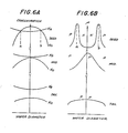
- the samples corresponded to normalized distances down the length of the crystal of 0.01, 0.12, 0.24 and 0.52. These four samples were chosen because they encompassed the three major resistivity forms.
- the three major forms are: (1) a doubly peaked profile with a p-n-p transition across the wafer diameter; (2) a singly peaked profile with a high resistivity center but p-type everywhere and (3) an essentially flat curve with relatively low resistivity but p-type everywhere.
- the samples were first characterized for initial resistivity.
- the diameter of each was profiled using s the capacitive TDR technique. Measurements were made every six millimeters.
- the spatial resolution of the TDR system used was less than two millimeters.
- the TDR technique can be thought of as a pulsed spreading resistance measurement.
- a voltage step is propagated down the transmission line and is capacitively coupled to a small region of the wafer by means of a coaxial probe.
- the incident pulse and reflected pulse from the sample are monitored.
- the initial reflected amplitude is a function of the local bulk resistivity of the sample. Since these measurements were made prior to any thermal donor anneal, the resistivity values were a measure of both the intended dopant and the oxygen thermal donor complex.
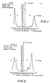
- the T D R results were checked on a fifth sample by doing additional mapping with the four point probe.
- The'TDR and four point probe results for this sample are shown in Fig. 5A and 5B respectively.
- the two techniques produced the same qualitative curve shape for this sample.
- With the four point probe a photo voltage effect was noted in the high resistivity regions. This led to typing of the wafers. It was found that there was a conductivity type change when going from the edge of the wafer to the center. There exists an outer p-type ring separated from an inner n-type disc by an annular intrinsic region.
- the three basic resistivity curve shapes can be explained as follows. Referring to Fig. 6A one sees that the thermal donors will compensate the intended p-type boron dopant. In the seed end of the crystal, the peak concentration of the thermal donors can exceed that of the boron. When this occurs, the material is converted to n-type. The annular intrinsic region would then be coincident with the points at which the donor and acceptor concentration were equal, points (a, b) in Fig. 6A.
- the double resistivity peak form was found for approximately the first 15% of the crystal.
- the flat resistivity form was reached at a point less than 50% down the crystal.
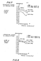
- Figs. 7-10 the initial oxygen concentration was measured at five or six points along a radius of each sample. The measurement was made on a Fourier transform infrared spectrometer. The IR absorbance is plotted in Figs. 7 and 8. Equivalent concentrations in parts per million are also indicated on the plots. The concentration is linearly related to the absorbance and inversely proportional to the thickness of the sample which, in this case, was about 0.7 mm.
- the oxygen concentration was fairly constant along the radius about one centimeter from the edge, at which point the concentration dropped by five to ten parts per million.
- the peak concentration in the center of the seed end was 40 ppm, dropping to 33 ppm by mid crystal.
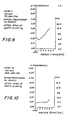
- FIGs. 7 and 8 two samples were subjected to thirty hours at 1000C in two steps. Each fifteen hour step was done in a dry oxygen ambient in an MOS qualified furnace. After each oxidation, the resulting 430 nm oxide was stripped, and infrared absorption measurements were made to determine the remaining interstitial oxygen concentration. These data are plotted in Figs. 7 and 8 along with the initial oxygen data. It will be seen in these figures that the greatest amount of precipitation occurred out near the edge of the wafer. It is easier to determine the amount of precipitation if one plots the difference, point by point, of the initial interstitial oxygen concentration and that after thirty hours of thermal processing. These data are plotted in Figs. 9 and 10.
- the oxygen precipitation profile for the samples 270-1 and 270-10, depicted in Fig. 9 and Fig. 10, respectively, is the result of a particular form of heat treatment, which operates to produce the greatest extent of precipitation in the annular region defined near the edge of the wafer. It is to be noted that a totally different form of heat treatment will bring about the opposite precipitation profile to that of Fig. 9 and Fig. 10, that is, a profile having a negative slope, rather than the positive slope exhibited. Thus, the least amount of precipitation will occur in the annular region near the edge and the greatest amount everywhere else.
- the technique is non-destructive in nature because it is performed on the wafers prior to any conventional annealing heat treatment; nevertheless, it yields an accurate prediction, based on initial resistivity measurements, of the final oxygen precipitation profile that will be obtained in those wafers.
Landscapes
- Chemical & Material Sciences (AREA)
- Chemical Kinetics & Catalysis (AREA)
- Electrochemistry (AREA)
- Physics & Mathematics (AREA)
- Health & Medical Sciences (AREA)
- Life Sciences & Earth Sciences (AREA)
- Analytical Chemistry (AREA)
- Biochemistry (AREA)
- General Health & Medical Sciences (AREA)
- General Physics & Mathematics (AREA)
- Immunology (AREA)
- Pathology (AREA)
- Testing Or Measuring Of Semiconductors Or The Like (AREA)
- Crystals, And After-Treatments Of Crystals (AREA)
Applications Claiming Priority (2)
| Application Number | Priority Date | Filing Date | Title |
|---|---|---|---|
| US06/235,207 US4342616A (en) | 1981-02-17 | 1981-02-17 | Technique for predicting oxygen precipitation in semiconductor wafers |
| US235207 | 2008-09-22 |
Publications (3)
| Publication Number | Publication Date |
|---|---|
| EP0058337A2 true EP0058337A2 (de) | 1982-08-25 |
| EP0058337A3 EP0058337A3 (en) | 1985-09-18 |
| EP0058337B1 EP0058337B1 (de) | 1988-12-14 |
Family
ID=22884552
Family Applications (1)
| Application Number | Title | Priority Date | Filing Date |
|---|---|---|---|
| EP82100720A Expired EP0058337B1 (de) | 1981-02-17 | 1982-02-02 | Verfahren für die Voraussage der Prezipitation von Sauerstoff in Halbleitersubstraten |
Country Status (4)
| Country | Link |
|---|---|
| US (1) | US4342616A (de) |
| EP (1) | EP0058337B1 (de) |
| JP (1) | JPS5833701B2 (de) |
| DE (1) | DE3279291D1 (de) |
Cited By (2)
| Publication number | Priority date | Publication date | Assignee | Title |
|---|---|---|---|---|
| EP0165364A1 (de) * | 1984-06-20 | 1985-12-27 | International Business Machines Corporation | Verfahren zum Standardisieren und Stabilisieren von Halbleiterscheiben |
| GB2324652A (en) * | 1997-04-23 | 1998-10-28 | Samsung Electronics Co Ltd | Method of analyzing a semiconductor ingot |
Families Citing this family (14)
| Publication number | Priority date | Publication date | Assignee | Title |
|---|---|---|---|---|
| US4559102A (en) * | 1983-05-09 | 1985-12-17 | Sony Corporation | Method for recrystallizing a polycrystalline, amorphous or small grain material |
| US4668330A (en) * | 1985-12-05 | 1987-05-26 | Monsanto Company | Furnace contamination |
| US4809196A (en) * | 1986-04-10 | 1989-02-28 | International Business Machines Corporation | Method for designating/sorting semiconductor wafers according to predicted oxygen precipitation behavior |
| US5066599A (en) * | 1989-07-27 | 1991-11-19 | Fujitsu Limited | Silicon crystal oxygen evaluation method using fourier transform infrared spectroscopy (ftir) and semiconductor device fabrication method using the same |
| JPH0862122A (ja) * | 1994-08-24 | 1996-03-08 | Komatsu Electron Metals Co Ltd | シリコンウェーハの酸素析出欠陥密度評価方法 |
| JP3446572B2 (ja) * | 1997-11-11 | 2003-09-16 | 信越半導体株式会社 | シリコン単結晶中の酸素析出挙動を割り出す方法、およびシリコン単結晶ウエーハ製造工程の決定方法、並びにプログラムを記録した記録媒体 |
| US7112509B2 (en) * | 2003-05-09 | 2006-09-26 | Ibis Technology Corporation | Method of producing a high resistivity SIMOX silicon substrate |
| US7521382B2 (en) * | 2005-05-19 | 2009-04-21 | Memc Electronic Materials, Inc. | High resistivity silicon structure and a process for the preparation thereof |
| CN102721697B (zh) * | 2012-05-29 | 2014-04-30 | 江西赛维Ldk太阳能高科技有限公司 | 一种晶体硅位错的检测方法及检测系统 |
| US9064823B2 (en) * | 2013-03-13 | 2015-06-23 | Taiwan Semiconductor Manufacturing Co., Ltd. | Method for qualifying a semiconductor wafer for subsequent processing |
| US10141413B2 (en) | 2013-03-13 | 2018-11-27 | Taiwan Semiconductor Manufacturing Co., Ltd. | Wafer strength by control of uniformity of edge bulk micro defects |
| US20150294868A1 (en) * | 2014-04-15 | 2015-10-15 | Infineon Technologies Ag | Method of Manufacturing Semiconductor Devices Containing Chalcogen Atoms |
| CN110389108A (zh) * | 2019-08-16 | 2019-10-29 | 西安奕斯伟硅片技术有限公司 | 一种单晶硅缺陷区域的检测方法及装置 |
| CN111380830A (zh) * | 2020-04-30 | 2020-07-07 | 西安奕斯伟硅片技术有限公司 | 一种单晶晶圆缺陷类型及分布区域的检测方法 |
Family Cites Families (4)
| Publication number | Priority date | Publication date | Assignee | Title |
|---|---|---|---|---|
| US3669757A (en) * | 1970-03-23 | 1972-06-13 | Ibm | Method of making and using diced single crystal impurity source |
| US3805160A (en) * | 1972-04-25 | 1974-04-16 | Ibm | Method for non-contact semiconductor resistivity measurement |
| US4140570A (en) * | 1973-11-19 | 1979-02-20 | Texas Instruments Incorporated | Method of growing single crystal silicon by the Czochralski method which eliminates the need for post growth annealing for resistivity stabilization |
| FR2460479A1 (fr) * | 1979-06-29 | 1981-01-23 | Ibm France | Procede de caracterisation de la teneur en oxygene des barreaux de silicium tires selon la methode czochralski |
-
1981
- 1981-02-17 US US06/235,207 patent/US4342616A/en not_active Expired - Fee Related
- 1981-12-11 JP JP56198704A patent/JPS5833701B2/ja not_active Expired
-
1982
- 1982-02-02 EP EP82100720A patent/EP0058337B1/de not_active Expired
- 1982-02-02 DE DE8282100720T patent/DE3279291D1/de not_active Expired
Cited By (3)
| Publication number | Priority date | Publication date | Assignee | Title |
|---|---|---|---|---|
| EP0165364A1 (de) * | 1984-06-20 | 1985-12-27 | International Business Machines Corporation | Verfahren zum Standardisieren und Stabilisieren von Halbleiterscheiben |
| GB2324652A (en) * | 1997-04-23 | 1998-10-28 | Samsung Electronics Co Ltd | Method of analyzing a semiconductor ingot |
| GB2324652B (en) * | 1997-04-23 | 2002-06-26 | Samsung Electronics Co Ltd | Method of analyzing a semiconductor ingot |
Also Published As
| Publication number | Publication date |
|---|---|
| JPS57139936A (en) | 1982-08-30 |
| US4342616A (en) | 1982-08-03 |
| JPS5833701B2 (ja) | 1983-07-21 |
| EP0058337A3 (en) | 1985-09-18 |
| EP0058337B1 (de) | 1988-12-14 |
| DE3279291D1 (en) | 1989-01-19 |
Similar Documents
| Publication | Publication Date | Title |
|---|---|---|
| EP0058337B1 (de) | Verfahren für die Voraussage der Prezipitation von Sauerstoff in Halbleitersubstraten | |
| US5961713A (en) | Method for manufacturing a wafer having a microdefect-free layer of a precisely predetermined depth | |
| JP6013449B2 (ja) | 格子間酸素濃度を決定する方法 | |
| JP3120825B2 (ja) | エピタキシャルウエーハ及びその製造方法 | |
| Rougieux et al. | Influence of annealing and bulk hydrogenation on lifetime-limiting defects in nitrogen-doped floating zone silicon | |
| Schwuttke | Silicon material problems in semiconductor device technology | |
| Lourenco et al. | Deep level transient spectroscopy of CdS/CdTe thin film solar cells | |
| Benson et al. | Characterization of Dislocations in (112) B HgCdTe/CdTe/Si | |
| EP0550750B1 (de) | Thermische behandlungsmethode für halbleiterscheiben | |
| CN110783218B (zh) | 一种碳化硅外延晶片掺杂浓度三轴型测试方法 | |
| Pearton et al. | Characterization of GaAs layers grown directly on Si substrates by metalorganic chemical vapor deposition | |
| US5598452A (en) | Method of evaluating a silicon single crystal | |
| US6803242B2 (en) | Evaluation method of IG effectivity in semiconductor silicon substrates | |
| Zhang et al. | Systematic investigation of shallow acceptor levels in ZnSe | |
| JP2005223098A (ja) | ドーパント汚染の評価方法及び熱処理工程の管理方法並びにドーパント汚染量の測定方法 | |
| Jungbluth | A review of bulk and process-induced defects in GaAs semiconductors | |
| EP3205625A1 (de) | Polykristallines silicium und verfahren zur auswahl von polykristallinem silicium | |
| US6586261B1 (en) | Method for determining a preceding wafer group | |
| Walz et al. | Characterization of nickel contamination in Float Zone and Czochralsky silicon wafers by using electrolytic metal tracer or microwave photoconductivity decay measurement | |
| JP4952871B2 (ja) | シリコンウェーハの評価方法 | |
| DE102020134992B4 (de) | Wafer-positionierungsverfahren | |
| WO2020233960A1 (de) | Verfahren zur herstellung von halbleiterscheiben | |
| Varker | Effects of Oxygen Precipitation on Minority Carrier Lifetime in | |
| US6013556A (en) | Method of integrated circuit fabrication | |
| JPH11297704A (ja) | 酸素析出物密度の評価方法 |
Legal Events
| Date | Code | Title | Description |
|---|---|---|---|
| PUAI | Public reference made under article 153(3) epc to a published international application that has entered the european phase |
Free format text: ORIGINAL CODE: 0009012 |
|
| AK | Designated contracting states |
Designated state(s): DE FR GB IT |
|
| 17P | Request for examination filed |
Effective date: 19821220 |
|
| PUAL | Search report despatched |
Free format text: ORIGINAL CODE: 0009013 |
|
| AK | Designated contracting states |
Designated state(s): DE FR GB IT |
|
| 17Q | First examination report despatched |
Effective date: 19870506 |
|
| GRAA | (expected) grant |
Free format text: ORIGINAL CODE: 0009210 |
|
| AK | Designated contracting states |
Kind code of ref document: B1 Designated state(s): DE FR GB IT |
|
| REF | Corresponds to: |
Ref document number: 3279291 Country of ref document: DE Date of ref document: 19890119 |
|
| PGFP | Annual fee paid to national office [announced via postgrant information from national office to epo] |
Ref country code: FR Payment date: 19890126 Year of fee payment: 8 |
|
| PGFP | Annual fee paid to national office [announced via postgrant information from national office to epo] |
Ref country code: GB Payment date: 19890131 Year of fee payment: 8 |
|
| ET | Fr: translation filed | ||
| PGFP | Annual fee paid to national office [announced via postgrant information from national office to epo] |
Ref country code: DE Payment date: 19890227 Year of fee payment: 8 |
|
| ITTA | It: last paid annual fee | ||
| ITF | It: translation for a ep patent filed | ||
| PLBE | No opposition filed within time limit |
Free format text: ORIGINAL CODE: 0009261 |
|
| STAA | Information on the status of an ep patent application or granted ep patent |
Free format text: STATUS: NO OPPOSITION FILED WITHIN TIME LIMIT |
|
| 26N | No opposition filed | ||
| PG25 | Lapsed in a contracting state [announced via postgrant information from national office to epo] |
Ref country code: GB Effective date: 19900202 |
|
| GBPC | Gb: european patent ceased through non-payment of renewal fee | ||
| PG25 | Lapsed in a contracting state [announced via postgrant information from national office to epo] |
Ref country code: FR Effective date: 19901031 |
|
| PG25 | Lapsed in a contracting state [announced via postgrant information from national office to epo] |
Ref country code: DE Effective date: 19901101 |
|
| REG | Reference to a national code |
Ref country code: FR Ref legal event code: ST |