EP0057549A2 - Halbleitervorrichtung - Google Patents
Halbleitervorrichtung Download PDFInfo
- Publication number
- EP0057549A2 EP0057549A2 EP82300367A EP82300367A EP0057549A2 EP 0057549 A2 EP0057549 A2 EP 0057549A2 EP 82300367 A EP82300367 A EP 82300367A EP 82300367 A EP82300367 A EP 82300367A EP 0057549 A2 EP0057549 A2 EP 0057549A2
- Authority
- EP
- European Patent Office
- Prior art keywords
- semiconductor
- region
- regions
- type
- layer
- Prior art date
- Legal status (The legal status is an assumption and is not a legal conclusion. Google has not performed a legal analysis and makes no representation as to the accuracy of the status listed.)
- Granted
Links
Images


Classifications
-
- H—ELECTRICITY
- H10—SEMICONDUCTOR DEVICES; ELECTRIC SOLID-STATE DEVICES NOT OTHERWISE PROVIDED FOR
- H10D—INORGANIC ELECTRIC SEMICONDUCTOR DEVICES
- H10D84/00—Integrated devices formed in or on semiconductor substrates that comprise only semiconducting layers, e.g. on Si wafers or on GaAs-on-Si wafers
- H10D84/60—Integrated devices formed in or on semiconductor substrates that comprise only semiconducting layers, e.g. on Si wafers or on GaAs-on-Si wafers characterised by the integration of at least one component covered by groups H10D10/00 or H10D18/00, e.g. integration of BJTs
- H10D84/641—Combinations of only vertical BJTs
- H10D84/642—Combinations of non-inverted vertical BJTs of the same conductivity type having different characteristics, e.g. Darlington transistors
-
- H—ELECTRICITY
- H10—SEMICONDUCTOR DEVICES; ELECTRIC SOLID-STATE DEVICES NOT OTHERWISE PROVIDED FOR
- H10D—INORGANIC ELECTRIC SEMICONDUCTOR DEVICES
- H10D62/00—Semiconductor bodies, or regions thereof, of devices having potential barriers
- H10D62/10—Shapes, relative sizes or dispositions of the regions of the semiconductor bodies; Shapes of the semiconductor bodies
- H10D62/13—Semiconductor regions connected to electrodes carrying current to be rectified, amplified or switched, e.g. source or drain regions
- H10D62/137—Collector regions of BJTs
-
- H—ELECTRICITY
- H10—SEMICONDUCTOR DEVICES; ELECTRIC SOLID-STATE DEVICES NOT OTHERWISE PROVIDED FOR
- H10D—INORGANIC ELECTRIC SEMICONDUCTOR DEVICES
- H10D84/00—Integrated devices formed in or on semiconductor substrates that comprise only semiconducting layers, e.g. on Si wafers or on GaAs-on-Si wafers
- H10D84/01—Manufacture or treatment
- H10D84/0112—Integrating together multiple components covered by H10D8/00, H10D10/00 or H10D18/00, e.g. integrating multiple BJTs
-
- H—ELECTRICITY
- H10—SEMICONDUCTOR DEVICES; ELECTRIC SOLID-STATE DEVICES NOT OTHERWISE PROVIDED FOR
- H10D—INORGANIC ELECTRIC SEMICONDUCTOR DEVICES
- H10D84/00—Integrated devices formed in or on semiconductor substrates that comprise only semiconducting layers, e.g. on Si wafers or on GaAs-on-Si wafers
- H10D84/01—Manufacture or treatment
- H10D84/02—Manufacture or treatment characterised by using material-based technologies
- H10D84/03—Manufacture or treatment characterised by using material-based technologies using Group IV technology, e.g. silicon technology or silicon-carbide [SiC] technology
- H10D84/038—Manufacture or treatment characterised by using material-based technologies using Group IV technology, e.g. silicon technology or silicon-carbide [SiC] technology using silicon technology, e.g. SiGe
-
- H—ELECTRICITY
- H10—SEMICONDUCTOR DEVICES; ELECTRIC SOLID-STATE DEVICES NOT OTHERWISE PROVIDED FOR
- H10D—INORGANIC ELECTRIC SEMICONDUCTOR DEVICES
- H10D84/00—Integrated devices formed in or on semiconductor substrates that comprise only semiconducting layers, e.g. on Si wafers or on GaAs-on-Si wafers
- H10D84/60—Integrated devices formed in or on semiconductor substrates that comprise only semiconducting layers, e.g. on Si wafers or on GaAs-on-Si wafers characterised by the integration of at least one component covered by groups H10D10/00 or H10D18/00, e.g. integration of BJTs
- H10D84/65—Integrated injection logic
- H10D84/658—Integrated injection logic integrated in combination with analog structures
-
- H10W10/031—
-
- H10W10/30—
Definitions
- This invention relates to an improved semiconductor body comprising both high breakdown voltage bipolar transistors and high speed semiconductor elements.
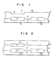
- Fig. 1 shows the construction of a prior art semiconductor body used for producing a semiconductor integrated circuit.
- an n -type epitaxial layer 2 is formed on a p -type semiconductor substrate 1.
- n +- type buried layers 3 1 and 3 2 are selectively formed at the interface between the substrate 1 and the epitaxial layer 2.
- a recess 4 is formed by etching in the surface region of the epitaxial layer 2 facing the n +- type buried layer 3 i , whith the result that the distance between the epitaxial layer surface and the buried layer is smaller in an epitaxial layer region 2 1 above the buried layer 3 1 than in an epitaxial layer region 2 2 above the buried layer 3 2 .
- high speed semiconductor elements is formed in the epitaxial layer region 2 1 , with high breakdown voltage semiconductor elements formed in the epitaxial layer region 2 2 , so as to form a semiconductor integrated circuit.
- the presence of the recess 4 renders it difficult to achieve fine processings in forming desired semiconductor elements in the epitaxial layer.
- Fig. 2 shows the construction of another prior art semiconductor body used for forming a semiconductor integrated circuit.
- an n -type first epitaxial layer 12 is formed on a p - -type semiconductor substrate 11.
- n +- type first buried layers 13 1 and 13 2 are selectively formed at the interface between the substrate 11 and the first epitaxial layer 12.
- the first buried layer 13 1 may be omitted in some cases.
- an n -type second epitaxial layer 14 is formed on the first epitaxial layer 12.
- an n +- type second buried layer 15 is formed at the interface between the first and second epitaxial layers 12 and 14 in a manner to face the first buried layer 13 1 .
- high speed semiconductor elements is formed in the second epitaxial layer 14 above the second buried layer 15, with high breakdown voltage semiconductor elements formed above the first buried layer 13 2 in a manner to extend through the first and second epitaxial layers 12 and 14.
- a p +- type isolation region or a dielectric film like an oxide film acting as an isolation region
- the epitaxial layer consisting of the layers 12 and 14 is so thick that it is necessary to apply a heat treatment at a high temperature for a long time for forming the p +- type isolation region mention above.
- the heat treatment mentioned causes a severe impurity diffusion from the buried layers 13 1 , 13 2 and 15, namely, the buried layers are expanded, rendering it very difficult to control as desired the distance between the surface of the second epitaxial layer 14 and the buried layers 15 or 13 2 .
- the highspeed and high breakdown voltage semiconductor elements formed between the second epitaxial layer surface and the buried layer 15 and between the second epitaxial layer surface and the buried layer 13 2 , respectively fail to perform satisfactory characteristics. It may be certainly possible to ensure a sufficient distance between the epitaxial layer surface and the buried layer by increasing the thickness of the epitaxial layer.
- the p +- type isolation region must be made deeper, leading to a severer heat treatment for forming the isolation region and, thus, to a greater expansion of the buried layer.
- the above-noted problem can not be solved by increasing the thickness of the epitaxial layer.
- the prior art shown in Fig. 1 also gives rise to the above-noted problem inherent in the prior art of Fig. 2.
- An object of this invention is to provide a semiconductor body with a smooth surface in which are formed both high breakdown voltage bipolar elements and high speed semiconductor elements performing satisfactory characteristics.
- a semiconductor body comprising
- This invention provides a semiconductor body comprising a first semiconductor layer of a first conductivity type formed on a semiconductor substrate of the first conductivity type, a second semiconductor layer of a second conductivity type formed on the first semiconductor layer, and a first semiconductor region of the second conductivity type formed between the surface of the first semiconductor layer and the substrate.
- the impurity concentration of the first semiconductor region is equal to or lower than that of the second semiconductor layer.
- the major element region of a high breakdown voltage bipolar transistor is formed within the first semiconductor region mentioned above. Also, it suffices to provide an isolation region of the first conductivity type in a manner to extend through the second semiconductor layer alone of the second conductivity type.
- the semiconductor body of the present invention permits markedly moderating the heat treating conditions, i.e., impurity diffusing conditions, for forming the isolation region, compared with the prior art shown in Fig. 2.
- the moderate heat treatment permits suppressing the impurity diffusion from the buried layers of high impurity concentration formed at the interface between the substrate and the first semiconductor layer and between the first and second semiconductor layers, rendering it possible to form both high breakdown voltage bipolar transistors and high speed semiconductor elements performing satisfactory characteristics.
- the breakdown voltage of the bipolar transistor is determined by the thickness of the first semiconductor layer.
- the thickness of the second semiconductor layer serves to determine the operating speed of the semiconductor elements formed together with the bipolar transistor mentioned above.
- the moderate heat treatment mentioned previously produces an additional effect.
- the lateral diffusion of impurity is suppressed in the step of forming the isolation region.
- the side diffusion of the isolation region can be suppressed, rendering it possible to increase the degree of integration of the produced semiconductor device.
- the upper surface of the semiconductor body i.e., the surface of the second semiconductor layer, is not provided with a recess but is smooth. Thus, it is possible to apply fine pattern processings to the semiconductor body. In addition, it is possible to prevent the breakage of the interconnection mounted to the semiconductor body.
- the semiconductor body of this invention permits producing a semiconductor device comprising bipolar transistors of high breakdown voltage and semiconductor elements operable at high speed.
- the produced semiconductor device is high in integration degree and in reliability.
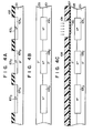
- Figs. 3A to 3I collectively show how to produce a semiconductor integrated circuit by utilizing the semiconductor body according to one embodiment of this invention.
- the integrated circuit comprises an npn bipolar transistor of high breakdown voltage, an npn bipolar transistor operable at high speed, and an integrated injection logic device operable at high speed.
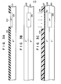
- Fig. 3A shows that an oxide film 102 is formed by thermal oxidation on the main surface of a p--type silicon substrate 101 having a resistivity of 1 to 20 ⁇ cm.
- the oxide film 102 is selectively etched away so as to provide an opening 103, followed by diffusing in a hot furnace an n-type impurity such as antimony or arsenic into the silicon substrate 101 thorugh the opening 103 so as to form an n +- type diffusion layer 104 having a sheet resistivity of 5 to 50 ⁇ / ⁇ .
- the remaining oxide film 102 is removed, followed by forming a p - -type epitaxial layer 105 having a thickness of 3 ⁇ m or more on the surface of the substrate 101 as shown in Fig. 3B.
- the epitaxial layer 105 has a resistivity of 1 ⁇ cm or more.
- the heat in the epitaxial growth step causes the impurity contained in the diffusion layer 104 to be diffused into the epitaxial layer 105 so as to form selectively an n +- type first buried layer 106 around the interface between the substrate 101 and the epitaxial layer 105.
- an oxide film 107 about 1,000 A thick is formed by thermal oxidation on the entire surface of the epitaxial layer 105 as shown in Fig. 3C, followed by forming a photoresist film 108 on the entire surface of the oxide film 107.
- the photoresist film 108 thus formed is selectively removed by photolithography so as to provide a window 109 above the buried layer 106.
- an n-type impurity of large diffusion coefficient e.g., phosphorus
- the photoresist film 108 is removed, followed by forming a SiO 2 film 111 about 1 ⁇ m thick on the thermal oxide film 107 as shown in Fig. 3D.
- the oxide film 111 which is formed by chemical vapor deposition, is annealed for 10 to 30 minutes at 900 to 1,100°C, followed by selectively etching the oxide film consisting of 107 and 111 so as to provide deffusion windows 112 1 , 112 2 and 112 3 .
- the window 112 1 is positioned to face the buried layer 106 at least partially.
- the windows 112 2 and 112 3 are sufficiently apart from the buried layer 106.
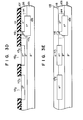
- an n-type impurity e.g., antimony or arsenic
- an n-type impurity e.g., antimony or arsenic
- an n + -type diffusion layer 113 1 having a sheet resistivity of 5 to 50 ⁇ / ⁇ and large n +- type diffusion layers 113 2 and 113 3 .
- the phosphous ion injection layer 110 (see Fig. 3C) is converted into an n - -type impurity region 114.
- the oxide films 111 and 107 are completely removed, followed by forming an n -type epitaxial layer 115 having a resistivity of 0.1 to 50 ⁇ cm and a thickness of 1 ⁇ m or more on the p - -type epitaxial layer 105 as shown in Fig. 3E.
- the heat in this epitaxial growth step causes the impurity contained in the n +- type diffusion layers 113 1 , 113 2 and 113 3 to be diffused into the n - -type epitaxial layer 115 so as to form n +- type buried layers 116, 117 1 and 117 2 around the interface between the p -type epitaxial layer 105 and the n - -type epitaxial layer 115 and, thus, to prepare a desired semiconductor body 118.
- the buried layer 116 is connected to the first buried layer 106 formed in advance as apparent from Fig. 3E.
- the buried layers 117 1 and 117 2 act as second buried layers.
- a p-type impurity e.g., boron
- a p-type impurity e.g., boron
- the isolation regions 119 extend across the n -type epitaxial layer 115 to reach the p -type epitaxial layer 105 so as to electrically divide the n -type epitaxial layer 115 into regions 115 1 , 115 2 and 115 3 .
- an n-type impurity e.g., phosphorus, arsenic or a mixture there of is selectively diffused into the divided regions 115 1 to 115 3 so as to form n + -type deep layers 120, 121 and 122 connected to the n +- type buried layers 116, 117 1 and 117 2 , respectively.
- the divided region 115 3 is surrounded by the n +- region consisting of the second buried layer 117 2 and the deep layer 122.
- a p-type impurity e.g., boron
- a p-type injector 124 and a p-type external base region 125 each extending to reach the n +- type second buried layer 117 2 are formed within the divided region 115 3 by means of ion implantation, followed by diffusion.
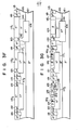
- the injector 124 and the external base region 125 are substantially equal in sheet resistivity to the base region 123.
- annular p-type external base region 126 having a sheet resistivity of 120 to 200 ⁇ / ⁇ is formed within the divided region 115 2 by means of ion plantation, followed by diffusion.
- the external base region 126 is shallower than the base region 123 formed in advance within the divided region 115 1 .
- a p -type internal base region 127 having a sheet resistivity of 300 to 1,000 ⁇ / ⁇ is formed in the region surrounded by the annular external base region 126 by means of ion implantation, followed by diffusion.
- p -type internal base regions 128 each having a sheet resistivity of 1 to 3 k ⁇ / ⁇ are formed in the regions surrounded by the external base regions 125 by means of ion implantation, followed by diffusion.
- the insulation film 129 formed on the entire surface as seen from Fig. 3H is selectively etched away so as to provide openings 130 1 to 130 6 , followed by forming on the entire surface a polycrystalline silicon (polysilicon) film 131 doped with an n-type impurity such as phosphorus, arsenic or both phosphorus and arsenic.
- the polysilicon film 131 is heated so as to allow the n-type impurity contained in the polysilicon film 131 to be diffused through the openings 130 1 to 130 6 into the semiconductor region so as to form an n +- type emitter region 132 within the base region 123 of the divided region 115 1 , to form an n +- type enlarged region 133 in the surface region of the n +- type deep layer 120 of the divided region 115 1 , to form an n +- type emitter region 134 within the p -type internal base region 127 of the divided region 115 2 , to form an n + -type enlarged region 135 in the surface region of the n +- type deep layer 121, and to form n +- type collector regions 136 1 and 136 2 within the p -type internal base regions 128 of the divided region 11 5 3 .
- the polysilicon film 131 is selectively etched away so as to allow the openings 130 1 to 130 6 alone to be filled with the remaining polysilicon film.
- a second insulation film 129' such as a CVD-Si0 2 film or a PSG film is formed on the entire surface followed by selectively removing the second insulation film 129' and the first and second insulation films 129 and 129' so as to provide contact holes 137 1 to 13 7 12 .
- a metal film e.g., At, Al-Si or Al-Si-Cu film, is formed on the entire surface by vacuum vapor deposition, followed by patterning the metal film so as to form the interconnections mounted to the semiconductor regions, as shown in Fig. 3I.
- the interconnections thus formed include an emitter electrode 138 connected via the polysilicon film 131 and the contact hole 137 1 to the n + -type emitter region 132 formed in the divided region 115 1 ; a base electrode 139 connected via the.contact hole 137 2 to the p +- type external base region 123; a collector electrode 140 connected via the polysilicon film 131 and the contact hole 137 3 to the n + -type region 133 communicating with the first buried layer 106; an emitter electrode 141 connected via the polysilicon film 131 and the contact hole 137 5 to the n +- type emitter region 134 formed in the divided region 115 2 ; a base electrode 142 connected via the contact hole 137 6 to the p-type external base region 126; a collector electrode 143 connected via the polysilicon film 131 and the contact hole 137 7 to the n +- type region 135 communicating with the second buried layer 117 1 ; an electrode 144 acting as a ground lead and connected via
- an npn bipolar transistor 149 of high breakdown voltage, an npn bipolar transistor 150 operable at high speed, and an I 2 L (Integrated Injection Logic) circuit 151 are formed in the divided regions 115 1 , 115 2 and 115 3 , respectively, as apparent from Fig. 3I.
- the semiconductor body 118 used for producing the semiconductor integrated circuit comprises a p -type semiconductor substrate 101, a p -type first semiconductor layer (epitaxial layer) 105 formed on the substrate 101, an n -type second semiconductor layer (epitaxial layer) 115 formed on the layer 105, and an n -type first semiconductor region (n -type in purity region) 114 formed between the surface of the p -type epitaxial layer 105 and the substrate 101, as seen from Figs. 3E and 3I.
- the impurity concentration of the region 114 is equal to or lower than that of the epitaxial layer 115.
- the major portion of the npn bipolar transistor 149 of high breakdown voltage is located in the n--type epitaxial layer 115 and the n--type inpurity region 114.
- the isolation region 119 it suffices for the isolation region 119 to extend across the n - -type epitaxial layer 115 alone, rendering it possible to shorten markedly the thermal diffusion treatment for prior art semiconductor body shown in Fig. 2.
- the buried layers 106, 117 1 and 117 2 i.e., second semiconductor region, third semiconductor regions
- the buried layers can be prevented from expansion in the step of forming the isolation region 119.
- the shortened heat treatment mentioned above also permits suppressing the lateral impurity diffusion so as to prevent the isolation region 119 from being expanded. As a result, it is possible to produce a semiconductor integrated circuit high in integration degree.
- the semiconductor body 118 has a smooth surface, rendering it possible to apply fine pattern processings for forming fine semiconductor regions like base regions,.emitter regions, etc.
- the n +- type diffusion layer 116 i.e., sixth semiconductor layer
- the diffusion layer 116 extends upward to enter the uppermost semiconductor layer, i.e., n -type epitaxial layer 115.
- the n +- type layer 120 need not be as deep as the thickness of the epitaxial layer 115.
- the small depth of the n +- type layer 120 permits markedly shortening the thermal diffusion time for forming the layer 120 and, thus, produces effects similar to those described previously in conjunction with the isolation region 119.
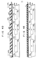
- Figs. 4A to 4I collectively show how to produce a semiconductor integrated circuit comprising an npn bipolar transistor of high breakdown voltage, an npn bipolar transistor operable at high speed, and an I 2 L circuit operable at high speed, by utilizing the semiconductor body according to another embodiment of this invention.
- Fig. 4A shows that an oxide film 102 is formed by thermal oxidation on the main surface of a p -type silicon substrate 101 having a resistivity of 1 to 25 ⁇ cm, followed by selectively etching the oxide film 102 so as to provide openings 103 1 to 103 3 . Then, an n-type impurity such as antimony or arsenic is selectively diffused within a hot furnace through the openings 103 1 to 103 3 into the substrate 101 so as to form n +- type diffusion layers 104 1 to 104 3 having a sheet resistivity of 5 to 50 ⁇ / ⁇ .
- an n-type impurity such as antimony or arsenic
- the remaining oxide film 102 is removed, followed by forming on the substrate surface a p - -type epitaxial layer 105 having a thickness of 3 ⁇ m or more and a resistivity of 1 ⁇ cm or more as shown in Fig. 4B.
- the heat in the epitaxial growth step causes the impurity contained in the diffusion layers 104 1 to 104 3 to be diffused into the epitaxial layer 105 so as to form n +- type first buried layers 106 1 to 106 3 around the interface between the substrate 101 and the epitaxial layer 105.
- a thermal oxide film 107 having a thickness 0 of about 1,000 A is formed on the entire surface of the epitaxial layer 105, followed by forming a photoresist film 108 on the oxide film 107 as shown in Fig. 4C.
- the photoresist film 108 thus formed is selectively removed by photolithography so as to provide a window 109 facing the first buried layer 106 1 , followed by introducing an n-type impurity, e.g., phosphorus, through the window 109 into the epitaxial layer 105 by ion implantation under an acceleration energy of 160 to 220 KeV and a dose of 1 to 30 x 10 11 cm -2 so as to form a phosphorus ion injection layer 110.
- an n-type impurity e.g., phosphorus
- the photoresist film 108 is removed, followed by forming again a photoresist film 108' as shown in Fig. 4D.
- the photoresist film 108' thus formed is selectively removed by photolithography so as to provide windows 109' 1 to 109' 4 , followed by selectively introducing boron, i.e., p-type impurity, into the epitaxial layer 105 through the windows 109' 1 to 109' 4 by ion implanation under an acceleration energy of 200 KeV and a dose of 1 to 100 x 10 14 cm -2 so as to form boron ion injection layers 152 1 to 152 4 positioned to surround the first buried layers 106 1 and 106 3 .
- boron i.e., p-type impurity
- the photoresist film 108' is removed, followed by forming a SiO 2 film 111 having a thickness of about 1 ⁇ m on the thermal oxide film 107 by chemical vapor deposition (CVD), as shown in Fig. 4E. Then, the oxide films 107 and 111 is selectively removed so as to provide a diffusion window 112 1 partially facing the n +- type first buried layer 106 1 and diffusion windows 112 2 and 112 3 facing the n +- type first buried layers 1062 and 1 063 , respectively.
- CVD chemical vapor deposition
- an n-type impurity e.g., antimony or arsenic
- an n-type impurity is selectively diffused through the diffusion windows 112 1 to 112 3 into the epitaxial layer 105 in a hot furnace so as to form n +- type diffusion layers 113 1 , 113 2 and 113 3 each having a sheet resistivity of 5 to 50 ⁇ / ⁇ .
- the diffusion layer 113 1 extends to reach the buried layer 106 1 .
- the diffusion layers 113 2 and 113 3 extend to reach the buried layers 106 2 and 106 3 , respectively.
- the impurity contained in the phosphorus ion injection layer 110 is diffused so as to convert the layer 110 into an n - -type impurity region 114 (see Fig. 4F). Also, the impurity contained in the boron ion injection layers 152 1 to 152 4 is diffused so as to convert the layers 152 1 to 152 4 into p + -type impurity regions 153 1 to 153 4 .
- the remaining oxide films 111 and 107 are entirely removed, followed by forming on the p -type epitaxial layer 105 an n -type epitaxial layer 115 having a resistivity of 0.1 to 50 ⁇ cm and a thickness of 1 ⁇ m or more as seen from Fig. 4G.
- the heat in the epitaxial growth step causes the impurity contained in the n +- type diffusion layers 113 1 to 113 3 to be diffused into the n - -type epitaxial layer 115 so as to form an n +- type diffusion layer 116.
- n + -type second buried layers 117 1 and 117 2 connected to the first buried layers 106 2 and 106 3 , respectively.
- the impurity contained in the p +- type impurity regions 153 1 to 153 4 is diffused into the n -type epitaxial layer 115 in the epitaxial growth step as seen from Fig. 4G so as to provide a desired semiconductor body 118'.
- a p-type impurity e.g., boron
- a p +- type isolation regions 119 connected to the p +- type impurity regions 153 1 to 153 4 formed previously as seen from Fig. 4H.
- the isolation regions 119 serve to electrically divide the epitaxial layer 115 into regions 115 1 , 115 2 and 115 3 .
- an n-type impurity e.g., phosphorus, arsenic or mixture of phosphorus and arsenic
- the layer 120 is connected to the n +- type first buried layer 106 1 via the diffusion region 116.
- the layers 121 and 122 are connected to the n + -type first buried layers 106 2 and 106 3 via the second buried layers 117 1 and 1172, respectively.
- the deep layer 122 is formed in a manner to surround the divided region 115 3 .
- a semiconductor integrated circuit comprising an npn bipolar transistor 149 of high breakdown voltage, an npn bipolar transistor 150 operable at high speed, and an I 2 L circuit 151 operable at high speed formed in the divided regions 115 1 , 115 2 and 115 3 , respectively as shown in Fig. 41 is produced as in Example 1.
- the n -type epitaxial layer 115 is electrically divided by the p +- type isolation regions 119.
- lateral parasitic transistors are formed by adjacent divided regions 115 1 to 115 3 and the p - -type epitaxial layer 105 below the n - -type epitaxial layer 115.
- the parasitic transistors formed between the divided regions 115 1 and 115 2 and between two adjacent transistors (not shown) of high breakdown voltage exhibit a considerably large value of current amplification factor.
- the p +- type impurity regions 153 1 to 153 4 (i.e., fifth semiconductor regions) connected to the p +- type isolation regions 119 extend across the p -type epitaxial layer 105, rendering it possible to suppress the formation of lateral parasitic transistors in question.
- the semiconductor integrated circuit is enabled to exhibit an improved reliablility.
- the p + -type impurity regions 153 1 to 153 4 extend into the n - -type epitaxial layer 115 as apparent from the drawing, leading to a shortened heat treatment for forming the p +- type isolation regions 119.
- the shortened heat treatment permits controlling as desired the characteristics of the produced semiconductor integrated circuit.
- n +- type first buried layers 106 2 and 106 3 serve to decrease the sheet resistivity of the n +- type second buried layers 117 1 and 117 2 connected to the layers 106 2 and 106 3 , respectively.
- the n -type impurity region 114 formed within the p -type epitaxial layer 105 is larger (or smaller) in width than the n +- type first buried layer 106 (or 106 1 ) positioned below the region 114.
- the width of the region 114 is made equal to or smaller (or larger) than that of the buried layer 106 (or 106 1 ) depending on the desired transistor characteristic, etc. of the integrated circuit.
- the n -type diffusion region 116 connected to the buried layer 106 (or 106 1 ) is formed within the n--type impurity region 114 in the Examples shown in the drawings.
- the isolation region 119 is formed of a p +- type diffusion layer. But, it is also possible to use a dielectric material for forming the isolation region 119. Of course, it sufficies for the dielectric material layer, i.e., isolation region, to extend across the n--type epitaxial layer 115, or to contact the p +- type impurity regions (153 1 to 153 4 ), rendering it possible to shorten the heat treatment for forming the isolation region and, thus, to suppress the impurity diffusion from the n +- type buried layer 117 1 , etc. Thus, the isolation region 119, even if formed of a dielectric material, permits producing the particular effects described previously in conjunction with Examples 1 and 2. The use of a dielectric material is particularly effective for producing a semiconductor device comprising both a transistor operable at high speed and a transistor of high breakdown voltage because of reducing the prasitic capacitance.
- the p-type base region 123 of the bipolar transistor 149 of high breakdown voltage is not in contact with the n--type impurity region 114.
- the base region 123 may be allowed to contact the n -type impurity region 114-.
- the base region 123 may be allowed to consist of a shallow internal base region low in impurity concentration and a deep external base region high in impurity concentration.
- the base regions of the transistors are formed separately from each other. However, it is possible to form a common base region depending on the desired transistor characteristics. For example, it is possible to make the external base region of the high breakdown voltage transistor common with the external base region of the I 2 L circuit. It is also possible to make the internal base region of the high breakdown voltage transistor common with the internal base region of the high speed transistor. The use of a common base region permits simplifying the manufacturing process of the semiconductor integrated circuit.
- a glass film doped with a low concentration of an n-type impurity e.g., phosphosilicate glass (PSG) film or arsenic-added glass (AsSG) film, is formed on the SiO 2 film 111 provided with a diffusion window.
- PSG or AsSG film thus ' formed is used as the diffusion source for diffusing phosphorus or arsenic into the p -type epitaxial layer 105 so as to form the n - -type impurity region 114.
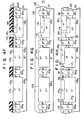
- Example 2 ion implantation technique is employed for forming the n -type impurity region 114 and the p +- type impurity regions 153 1 to 153 4 .
- the ion implantation technique may be replaced by impurity diffusion technique in Example 2, too, as seen from Fig. 5.
- the thermal oxide film 107.having o . a thickness of about 3,000 A formed on the p -type epitaxial layer 105 is selectively removed to provide the diffusion windows 154 1 , 154 3 to 154 5 , followed by forming a boron-added glass (BSG) film 155 on the entire surface.
- BSG boron-added glass
- the BSG film 155 is selectively removed from the diffusion window 154 2 , followed by forming a PSG film 156 on the entire surface.
- the BSG film 155 and the PSG film 156 thus formed are used as the diffusion sources for forming in the p--type epitaxial layer 105 the n - -type impurity region 114 and the p +- type impurity regions 153 1 to 153 4 in a single or more heating step.
- ion implantation technique is employed for forming the base regions of the transistors in the Examples shown in the drawings. But, the ion implantation technique may be replaced by thermal diffusion technique which utilizes an insulation film doped with a p-type impurity, e.g., BSG film, as the diffusion source.
- a p-type impurity e.g., BSG film
- resistivity of the base region described previously in conjunction with.Examples 1 and 2 may be changed freely depending on the desired operation characteristics of the resultant transistors.
- the conductivity type of the semiconductor regions may be reversed, i.e., the p-type and n-type regions may be changed into n-type and p-type regions, respectively, in the Examples shown in the drawings. Even if the conductivity type is reversed, the resultant semiconductor device produces effects similar to those described previously.
- a logic circuit such as an emitter coupled logic (ECL) circuit may be formed in place of the high speed npn bipolar transistor and the I 2 L circuit formed in the Examples shown in the drawings. It is also possible to form uni-junction transistors like MOS-FETs together with the npn bipolar transistor of high breakdown voltage.
- the semiconductor body of this invention permits producing a semiconductor integrated circuit comprising, for example, a bipolar transistor of high breakdown voltage, a bipolar . transistor operable at high speed, and an I 2 L circuit operable at high speed.
- a semiconductor integrated circuit comprising, for example, a bipolar transistor of high breakdown voltage, a bipolar . transistor operable at high speed, and an I 2 L circuit operable at high speed.
- the integrated circuit mentioned is high in integration density and in reliablility.
Landscapes
- Element Separation (AREA)
- Bipolar Integrated Circuits (AREA)
- Bipolar Transistors (AREA)
Applications Claiming Priority (6)
| Application Number | Priority Date | Filing Date | Title |
|---|---|---|---|
| JP56012094A JPS57126162A (en) | 1981-01-29 | 1981-01-29 | Semiconductor device |
| JP12094/81 | 1981-01-29 | ||
| JP56106515A JPS589356A (ja) | 1981-07-08 | 1981-07-08 | 半導体装置 |
| JP106514/81 | 1981-07-08 | ||
| JP56106514A JPS589354A (ja) | 1981-07-08 | 1981-07-08 | 半導体装置 |
| JP106515/81 | 1981-07-08 |
Publications (3)
| Publication Number | Publication Date |
|---|---|
| EP0057549A2 true EP0057549A2 (de) | 1982-08-11 |
| EP0057549A3 EP0057549A3 (en) | 1983-07-27 |
| EP0057549B1 EP0057549B1 (de) | 1987-07-29 |
Family
ID=27279698
Family Applications (1)
| Application Number | Title | Priority Date | Filing Date |
|---|---|---|---|
| EP82300367A Expired EP0057549B1 (de) | 1981-01-29 | 1982-01-25 | Halbleitervorrichtung |
Country Status (2)
| Country | Link |
|---|---|
| EP (1) | EP0057549B1 (de) |
| DE (1) | DE3276888D1 (de) |
Cited By (4)
| Publication number | Priority date | Publication date | Assignee | Title |
|---|---|---|---|---|
| DE3532380A1 (de) * | 1985-09-11 | 1987-03-12 | Bosch Gmbh Robert | Monolithisch integrierte halbleiteranordnung |
| US4780425A (en) * | 1985-04-19 | 1988-10-25 | Sanyo Electric Co., Ltd. | Method of making a bipolar transistor with double diffused isolation regions |
| EP0351331A1 (de) * | 1988-07-13 | 1990-01-17 | STMicroelectronics S.A. | Integrierte Schaltungsstruktur, die die Isolation zwischen Bauelementen verbessert |
| US5095355A (en) * | 1986-12-01 | 1992-03-10 | Mitsubishi Denki Kabushiki Kaisha | Bipolar cross-coupled memory cells having improved immunity to soft errors |
Family Cites Families (6)
| Publication number | Priority date | Publication date | Assignee | Title |
|---|---|---|---|---|
| JPS5633864B2 (de) * | 1972-12-06 | 1981-08-06 | ||
| IT1088974B (it) * | 1977-01-12 | 1985-06-10 | Rca Corp | Struttura a semiconduttori comprendente dispositivi per applicazioni a bassa tensione e ad alta tensione e metodo di preparazione della stessa |
| US4266238A (en) * | 1977-03-11 | 1981-05-05 | Zaidan Hojin Handotai Kenkyu Shinkokai | Semiconductor device having high-speed operation and integrated circuit using same |
| US4202006A (en) * | 1978-02-15 | 1980-05-06 | Rca Corporation | Semiconductor integrated circuit device |
| FR2436501A1 (fr) * | 1978-09-15 | 1980-04-11 | Thomson Csf | Transistors bipolaires a tension elevee, circuits integres comportant de tels transistors, et procede de fabrication de tels circuits |
| IT1101096B (it) * | 1978-12-22 | 1985-09-28 | Ates Componenti Elettron | Perfezionamento al procedimento per produrre dispositivi integrati a semiconduttore e prodotto risultante |
-
1982
- 1982-01-25 DE DE8282300367T patent/DE3276888D1/de not_active Expired
- 1982-01-25 EP EP82300367A patent/EP0057549B1/de not_active Expired
Cited By (5)
| Publication number | Priority date | Publication date | Assignee | Title |
|---|---|---|---|---|
| US4780425A (en) * | 1985-04-19 | 1988-10-25 | Sanyo Electric Co., Ltd. | Method of making a bipolar transistor with double diffused isolation regions |
| DE3532380A1 (de) * | 1985-09-11 | 1987-03-12 | Bosch Gmbh Robert | Monolithisch integrierte halbleiteranordnung |
| US5095355A (en) * | 1986-12-01 | 1992-03-10 | Mitsubishi Denki Kabushiki Kaisha | Bipolar cross-coupled memory cells having improved immunity to soft errors |
| EP0351331A1 (de) * | 1988-07-13 | 1990-01-17 | STMicroelectronics S.A. | Integrierte Schaltungsstruktur, die die Isolation zwischen Bauelementen verbessert |
| FR2634321A1 (fr) * | 1988-07-13 | 1990-01-19 | Sgs Thomson Microelectronics | Structure de circuit integre ameliorant l'isolement entre composants |
Also Published As
| Publication number | Publication date |
|---|---|
| EP0057549A3 (en) | 1983-07-27 |
| DE3276888D1 (en) | 1987-09-03 |
| EP0057549B1 (de) | 1987-07-29 |
Similar Documents
| Publication | Publication Date | Title |
|---|---|---|
| US4819052A (en) | Merged bipolar/CMOS technology using electrically active trench | |
| US4256515A (en) | Method for making integrated circuit with C-MOS logic, bipolar driver and polysilicon resistors | |
| US5006476A (en) | Transistor manufacturing process using three-step base doping | |
| US4884117A (en) | Circuit containing integrated bipolar and complementary MOS transistors on a common substrate | |
| EP0219831B1 (de) | Verfahren zur Herstellung von integrierten Halbleiterschaltungen mit einem bipolaren Transistor und einem Feldeffekttransistor mit isolierter Steuerelektrode | |
| US4176368A (en) | Junction field effect transistor for use in integrated circuits | |
| EP0083816B1 (de) | Halbleiteranordnung mit einem Verbindungsmuster | |
| EP0001300B1 (de) | Verfahren zur Herstellung einer LOCOS Halbleitervorrichtung | |
| US4412378A (en) | Method for manufacturing semiconductor device utilizing selective masking, etching and oxidation | |
| US4797372A (en) | Method of making a merge bipolar and complementary metal oxide semiconductor transistor device | |
| GB2148591A (en) | Semiconductor device isolation grooves | |
| US5554554A (en) | Process for fabricating two loads having different resistance levels in a common layer of polysilicon | |
| JPS622708B2 (de) | ||
| EP0078220B1 (de) | Polykristalline Silizium-Verbindungen für Bipolartransistoren in Flip-Flop-Schaltung | |
| EP0193934B1 (de) | Integrierte Halbleiterschaltungsanordnung und Verfahren zu ihrer Herstellung | |
| EP0017377B1 (de) | Verfahren zur Herstellung isolierter bipolarer Transistoren | |
| EP0337823A2 (de) | MOS-Feldeffekttransistor mit hoher Durchbruchspannung | |
| JP3228609B2 (ja) | 半導体装置及びその製造方法 | |
| EP0057549A2 (de) | Halbleitervorrichtung | |
| EP0337720B1 (de) | Verfahren zur Herstellung eines Bipolartransistors | |
| US5198373A (en) | Process for fabricating a semiconductor device | |
| US5023690A (en) | Merged bipolar and complementary metal oxide semiconductor transistor device | |
| US5350939A (en) | Semiconductor device and method of manufacturing thereof | |
| EP0718891B1 (de) | Hochleistungs-, Hochspannungs-, nicht-epitaxialer Bipolartransistor | |
| JPH0691192B2 (ja) | 接合電界効果トランジスタとキャパシタを形成する方法 |
Legal Events
| Date | Code | Title | Description |
|---|---|---|---|
| PUAI | Public reference made under article 153(3) epc to a published international application that has entered the european phase |
Free format text: ORIGINAL CODE: 0009012 |
|
| 17P | Request for examination filed |
Effective date: 19820205 |
|
| AK | Designated contracting states |
Designated state(s): DE FR GB NL |
|
| PUAL | Search report despatched |
Free format text: ORIGINAL CODE: 0009013 |
|
| AK | Designated contracting states |
Designated state(s): DE FR GB NL |
|
| RAP1 | Party data changed (applicant data changed or rights of an application transferred) |
Owner name: KABUSHIKI KAISHA TOSHIBA |
|
| GRAA | (expected) grant |
Free format text: ORIGINAL CODE: 0009210 |
|
| AK | Designated contracting states |
Kind code of ref document: B1 Designated state(s): DE FR GB NL |
|
| ET | Fr: translation filed | ||
| REF | Corresponds to: |
Ref document number: 3276888 Country of ref document: DE Date of ref document: 19870903 |
|
| PLBE | No opposition filed within time limit |
Free format text: ORIGINAL CODE: 0009261 |
|
| STAA | Information on the status of an ep patent application or granted ep patent |
Free format text: STATUS: NO OPPOSITION FILED WITHIN TIME LIMIT |
|
| 26N | No opposition filed | ||
| PGFP | Annual fee paid to national office [announced via postgrant information from national office to epo] |
Ref country code: FR Payment date: 19970109 Year of fee payment: 16 |
|
| PGFP | Annual fee paid to national office [announced via postgrant information from national office to epo] |
Ref country code: GB Payment date: 19970116 Year of fee payment: 16 |
|
| PGFP | Annual fee paid to national office [announced via postgrant information from national office to epo] |
Ref country code: NL Payment date: 19970130 Year of fee payment: 16 |
|
| PGFP | Annual fee paid to national office [announced via postgrant information from national office to epo] |
Ref country code: DE Payment date: 19970131 Year of fee payment: 16 |
|
| PG25 | Lapsed in a contracting state [announced via postgrant information from national office to epo] |
Ref country code: GB Free format text: LAPSE BECAUSE OF NON-PAYMENT OF DUE FEES Effective date: 19980125 |
|
| PG25 | Lapsed in a contracting state [announced via postgrant information from national office to epo] |
Ref country code: FR Free format text: THE PATENT HAS BEEN ANNULLED BY A DECISION OF A NATIONAL AUTHORITY Effective date: 19980131 |
|
| PG25 | Lapsed in a contracting state [announced via postgrant information from national office to epo] |
Ref country code: NL Free format text: LAPSE BECAUSE OF NON-PAYMENT OF DUE FEES Effective date: 19980801 |
|
| GBPC | Gb: european patent ceased through non-payment of renewal fee |
Effective date: 19980125 |
|
| NLV4 | Nl: lapsed or anulled due to non-payment of the annual fee |
Effective date: 19980801 |
|
| PG25 | Lapsed in a contracting state [announced via postgrant information from national office to epo] |
Ref country code: DE Free format text: LAPSE BECAUSE OF NON-PAYMENT OF DUE FEES Effective date: 19981001 |
|
| REG | Reference to a national code |
Ref country code: FR Ref legal event code: ST |