EP0054434A2 - Halbleiterbauelement - Google Patents
Halbleiterbauelement Download PDFInfo
- Publication number
- EP0054434A2 EP0054434A2 EP81305880A EP81305880A EP0054434A2 EP 0054434 A2 EP0054434 A2 EP 0054434A2 EP 81305880 A EP81305880 A EP 81305880A EP 81305880 A EP81305880 A EP 81305880A EP 0054434 A2 EP0054434 A2 EP 0054434A2
- Authority
- EP
- European Patent Office
- Prior art keywords
- contact window
- window
- layer
- atoms
- semiconductor device
- Prior art date
- Legal status (The legal status is an assumption and is not a legal conclusion. Google has not performed a legal analysis and makes no representation as to the accuracy of the status listed.)
- Granted
Links
Images


Classifications
-
- H—ELECTRICITY
- H10—SEMICONDUCTOR DEVICES; ELECTRIC SOLID-STATE DEVICES NOT OTHERWISE PROVIDED FOR
- H10D—INORGANIC ELECTRIC SEMICONDUCTOR DEVICES
- H10D1/00—Resistors, capacitors or inductors
- H10D1/40—Resistors
- H10D1/43—Resistors having PN junctions
-
- H—ELECTRICITY
- H10—SEMICONDUCTOR DEVICES; ELECTRIC SOLID-STATE DEVICES NOT OTHERWISE PROVIDED FOR
- H10D—INORGANIC ELECTRIC SEMICONDUCTOR DEVICES
- H10D64/00—Electrodes of devices having potential barriers
-
- H10D64/0111—
Definitions
- the present invention relates to a semiconductor device, more particularly, to an electric contact between a region of _ a semiconductor substrate and a conductive metal layer extending thereover.
- each resistor member is realized as a resistive diffusion layer formed in the semiconductor substrate, especially, as a diffusion layer having one conductivity in a silicon . substrate having the other conductivity.
- the resistor member is, then, connected to a conductive metal layer formedoverthe semiconductor substrate, via the electric contact, so as to cooperate with another corresponding - electric functional member or members.
- the resistance value (R) is mainly determined by the resistance value (R d ) of the resistive diffusion layer and, secondarily, by the ohmic contact resistance value (R ) created at the electric contact.
- the actual resistance value (R) is defined as being a sum of the above-mentioned two resistance values (R d ) and (R c ). Accordingly, if the resistance value (R) must be strictly set to a predetermined value, not only the resistance value (R d ), but also the resistance value (R ), must also be strictly set so as to obtain the exact desired resistance value (R)'.
- Fig. 1 is an example of a circuit diagram which must contain therein resistor members having exactly correct resistance values.
- the example of this figure represents the so-called current mirror circuit.
- the circuit is comprised of three transistors T 1 , T 2 , T 3 , four resistor members R 0 , R 1 , R 2 , R 3 and two loads L 2 , L 3 .
- the symbols I 1 , I 2 and I denote currents flowing in those respective paths.
- the current mirror circuit is inserted between the power supply voltage level V cc and the ground level GND.
- Fig. 2 illustrates a plan view of a semiconductor circuit for fabricating the current mirror circuit of Fig. 1.
- the above-mentioned ratio of the current values is set at 1, and, accordingly, the ratio of the resistance values is also set at 1. Therefore, the transistors T 1 , T 2 'and T 3 have the same physical conditions and also the resistor members R 1 , R 2 and R 3 have the same physical conditions.
- the transistors T 1 , T 2 and T 3 are formed inside respective islands which are enclosed by an isolation area I SO .
- the reference symbols C represent N-type collector regions. Each of the collector regions C is connected to a respective conductive metal layer MC via a respective .collector contact window CCW.
- the reference symbols B represent P-type base regions. These three base regions B are commonly connected by a conductive metal layer M B , via respective base contact windows BCW.
- the reference symbols E represent N-type emitter regions formed in the respective base regions B. Each of the emitter regions E is connected to a first conductive metal layer M E1 , via respective emitter contact windows ECW.
- the resistor members R 1 , R 2 and R 3 are formed inside an island which is also enclosed by the isolation area I SO . This island is formed as an N-type region IS.
- the resistor members R 1 , R 2 and R 3 are made of respective P-type resistive diffusion layers RD, located inside the island IS.
- Each of the resistive diffusion layers RD is connected, on the one hand, to the first conductive metal layer M E1 via respective resistor contact windows RCW and connected, on the other hand, to a second conductive metal layer M E2 , via respective resistor contact windows RCW.
- the metal layer M E2 comprises the ground level GND of Fig. 1.
- the resistor members R 1 , R 2 and R 3 must be exactly identical to each other so as to supply the currents I 1 , I 2 and I3 with the exact same value.
- the previously mentioned ratio of currents is 1. Consequently, when designing a current mirror circuit, a designer usually designs the resistive diffusion layers RD to be physically identical with each other, and also designs the resistor contact windows RCW to be physically identical with each other.
- each layer RD is the size of each layer RD and also the size of each window RCW:
- the actual resistance value (R) is defined as being the sum of the resistance value, in series, of the resistor (R d ), which corresponds to the resistive diffusion layer RD, and the resistance value (R C ), which corresponds to the ohmic contact at the resistor contact window RCW.
- the resistance value (R d ) of the former is constant'and does not vary once the diffusion layer RD is produced. Contrary to this, the resistance value (R ) of the latter is not constant and varies over a long period of time.
- the resistance value (R ) of the ohmic contact initially has a certain value when the manufacturing process has finished. However, thereafter, the resistance value (R ) varies due to the aforementioned diffusion of the Si atoms into the gaps between the Al atoms in the A1 layer.
- the Si atoms and the A l atoms respectively compose the layer RD and the layer M E2 (also M E1 ). To be more specific, over a long period of time, the Si atoms gradually penetrate into the gaps between the Al atoms. As will be apparent from this, even though the resistor members R 1 , R 2 and R 3 have been manufactured to be the exact same design, the resistance values thereof will be changed over a long period of time, due to the diffusion of the Si atoms into the Al layer.
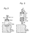
- Fig. 3 illustrates a partial plan view of Fig. 2, indicating one of the resistors and its neighboring members.
- Fig. 4 illustrates an enlarged cross-sectional view taken along the line 4-4 shown in Fig. 3.
- a semiconductor substrate 40 is comprised of a P-type semiconductor substrate'41 and an N-type semiconductor substrate 42 formed thereon.
- the P-type resistive diffusion layer RD is formed in the N-type substrate 42 and extended along the surface thereof.
- the resistive diffusion layer RD is connected to the conductive metal layers M El and M E2 via the respective resistor contact windows RCW.
- the resistor contact windows RCW are formed in an insulation layer 43.
- the actual resistance value R of the resistor member shown in Figs. 3 and 4 is determined as being the sum of the resistance value R d (shown in Fig. 4) and the resistance values (R C ) (not shown in Fig. 4) at the resistor contact windows RCW, that is the ohmic contact resistors.
- the present invention is specifically directed to such resistance values (R ). This is because the resistance values (R ) are liable to vary due to the aforesaid diffusion of the Si atoms. It should also be noted that such variation of the resistance value (R ) at the window RCW (right side) is larger than that of the value (R ) at the window RCW (left side).
- the Si atoms are liable to drift along the area that has a high gradient of Si density in the Al layer.
- the gradient of Si density in the Al layer M E2 is higher than that of Si density in the Al layer M E1 , because the mass of the Al layer M E2 is much larger than that of the Al layer M E1 , as clearly shown in Fig. 2, which Fig. 2 illustrates a large mass of the A1 layer M E2 acting as a ground bus.
- the resistance value at the window RCW for the layer M E2 is liable to vary.
- the area where the resistance value is most likely to vary is at a peripheral portion 44, enclosed by a dotted circle in Fig. 4, of the window RCW.
- Fig. 5 illustrates a partial plan view of a semiconductor device, embodying the present invention, which is to be compared with the device shown in Fig. 3.
- Fig. 6 illustrates an enlarged cross-sectional view taken along the line 6-6 shown in Fig. 5.
- a Si atom supplier is located close to the resistor contact window RC W .
- S i atom supplier is realized by a dummy resistor contact window DRCW.
- this auxiliary window DRCW is located in and along a path of a Si atom flow.
- the Si atom flow is created through the previously mentioned gradient of Si atom density in the Al layer. Therefore, the Si atoms flow from the windows RCW,DRCW toward the Al ground bus (GND).
- the dummy window DRCW is positioned between the real window RCW and the Al layer M E2 (GND).
- the Si atoms travel from the window RCW toward the Al layer M E2 of Fig. 5, as schematically illustrated by an arrow. It is known that Si. diffusion into an Al layer continues until the Al layer is saturated with Si. Saturation usually occurs at the density of 1%. This Si density around the window RCW could be quickly attained,- provided that such saturation is not prevented by a continued Si atom flow from window RCW to.the large mass of the layer M E2 .
- the Si atom diffusion into the Al layer from the real window is stabilized after the above mentioned saturation of Si atom is achieved in and around each of the windows RCW and DRCW.
- Such areas of saturation may be obtained during the ordinary manufacturing process of the corresponding semiconductor devices by utilizing for example a heat treatment.
- Si diffusion in and around the window RCW, especially at the portion 44 can be prevented over a long period of time; thereby, the corresponding resistance value is maintained at a fixed value.
- the narrow Al layers M E ' and M E " are more useful for slowing down the aforesaid Si atom flow toward the layer (GND), when compared with wide Al layers of the prior art.
- Fig. 7 illustrates a partial plan view of a second embodiment of the present invention.
- the resistor contact window RCW and the dummy resistor contact window DRCW are formed as one body, but are slightly separated from each other by means of the narrow conductive metal layer ME'.
- the insulation layer 43 (referring back to Fig. 6), located between the windows RCW and DRCW, is not necessary.
- the configuration of the dummy resistor contact window can freely be selected at will. At any rate, the configuration of the window is not so important - as long as the Si diffusion into the Al layer, especially at the peripheral portion 44, is stopped.
- Fig. 8 illustrates a partial plan view of a third embodiment of the present invention, which is comparable with the device shown in Fig. 3.
- Fig. 9 illustrates an enlarged cross-sectional view taken along the line 9-9 shown in Fig. 8.
- the members represented by the same reference symbols and numerals are respectively identical to those of Figs. 5, 6 and 7.
- the resistor contact window RCW is divided, for example, into three resistor contact windows RCW . , RCW and RCW 3 , and these are arranged along the peripheral portion 44.
- the resistor contact window RCW is divided into three windows RCW , RCW and RCW 3 , adapted to form barriers therebetween. The barriers are referenced by 43' and 43" in Fig.
Landscapes
- Semiconductor Integrated Circuits (AREA)
- Electrodes Of Semiconductors (AREA)
- Engineering & Computer Science (AREA)
- Physics & Mathematics (AREA)
- Condensed Matter Physics & Semiconductors (AREA)
- General Physics & Mathematics (AREA)
- Manufacturing & Machinery (AREA)
- Computer Hardware Design (AREA)
- Microelectronics & Electronic Packaging (AREA)
- Power Engineering (AREA)
Applications Claiming Priority (2)
| Application Number | Priority Date | Filing Date | Title |
|---|---|---|---|
| JP55176672A JPS57100755A (en) | 1980-12-15 | 1980-12-15 | Semiconductor device |
| JP176672/80 | 1980-12-15 |
Publications (3)
| Publication Number | Publication Date |
|---|---|
| EP0054434A2 true EP0054434A2 (de) | 1982-06-23 |
| EP0054434A3 EP0054434A3 (en) | 1983-01-12 |
| EP0054434B1 EP0054434B1 (de) | 1986-05-28 |
Family
ID=16017694
Family Applications (1)
| Application Number | Title | Priority Date | Filing Date |
|---|---|---|---|
| EP81305880A Expired EP0054434B1 (de) | 1980-12-15 | 1981-12-15 | Halbleiterbauelement |
Country Status (5)
| Country | Link |
|---|---|
| US (1) | US4757368A (de) |
| EP (1) | EP0054434B1 (de) |
| JP (1) | JPS57100755A (de) |
| DE (1) | DE3174745D1 (de) |
| IE (1) | IE52806B1 (de) |
Families Citing this family (4)
| Publication number | Priority date | Publication date | Assignee | Title |
|---|---|---|---|---|
| JPH02114533A (ja) * | 1988-10-24 | 1990-04-26 | Nec Corp | 半導体装置 |
| KR100462878B1 (ko) * | 2002-03-22 | 2004-12-17 | 삼성전자주식회사 | 길이가 긴 부하저항을 구비한 반도체 장치 및 그의 제조방법 |
| JP3927111B2 (ja) * | 2002-10-31 | 2007-06-06 | 株式会社東芝 | 電力用半導体装置 |
| US9202859B1 (en) * | 2014-05-27 | 2015-12-01 | Texas Instruments Incorporated | Well resistors and polysilicon resistors |
Family Cites Families (20)
| Publication number | Priority date | Publication date | Assignee | Title |
|---|---|---|---|---|
| US3559003A (en) * | 1969-01-03 | 1971-01-26 | Ibm | Universal metallurgy for semiconductor materials |
| GB1250988A (de) * | 1969-08-14 | 1971-10-27 | ||
| DE2018589A1 (en) * | 1970-04-17 | 1971-10-28 | Siemens Ag | Aluminium metallising of silicon surfaces |
| US3629782A (en) * | 1970-10-06 | 1971-12-21 | Cogar Corp | Resistor with means for decreasing current density |
| JPS4875169A (de) * | 1972-01-12 | 1973-10-09 | ||
| CA997481A (en) * | 1972-12-29 | 1976-09-21 | International Business Machines Corporation | Dc testing of integrated circuits and a novel integrated circuit structure to facilitate such testing |
| US4051391A (en) * | 1974-04-24 | 1977-09-27 | Rca Corporation | Current-operated circuits and structures |
| US4131809A (en) * | 1974-06-17 | 1978-12-26 | U.S. Philips Corporation | Symmetrical arrangement for forming a variable alternating-current resistance |
| US4022931A (en) * | 1974-07-01 | 1977-05-10 | Motorola, Inc. | Process for making semiconductor device |
| JPS51151572U (de) * | 1975-05-27 | 1976-12-03 | ||
| IT1038800B (it) * | 1975-06-10 | 1979-11-30 | Ates Componenti Elettron | Tranistore planare di potenza |
| JPS5279887A (en) * | 1975-12-26 | 1977-07-05 | Fujitsu Ltd | Production of semiconductor device |
| JPS5384579A (en) * | 1976-12-29 | 1978-07-26 | Fujitsu Ltd | Manufacture for semiconductor device |
| IT1115654B (it) * | 1977-05-04 | 1986-02-03 | Ates Componenti Elettron | Partitore di tensione diffuso per circuito integrato monolitico |
| FR2413782A1 (fr) * | 1977-12-30 | 1979-07-27 | Radiotechnique Compelec | Element de circuit integre destine aux memoires bipolaires a isolement lateral par oxyde |
| JPS551103A (en) * | 1978-06-06 | 1980-01-07 | Chiyou Lsi Gijutsu Kenkyu Kumiai | Semiconductor resistor |
| IT1096633B (it) * | 1978-06-13 | 1985-08-26 | Ates Componenti Elettron | Resistore diffuso in un corpo semiconduttore |
| US4215333A (en) * | 1978-10-02 | 1980-07-29 | National Semiconductor Corporation | Resistor termination |
| US4219797A (en) * | 1979-03-19 | 1980-08-26 | National Semiconductor Corporation | Integrated circuit resistance ladder having curvilinear connecting segments |
| JPS55138273A (en) * | 1979-04-11 | 1980-10-28 | Fujitsu Ltd | Transistor |
-
1980
- 1980-12-15 JP JP55176672A patent/JPS57100755A/ja active Granted
-
1981
- 1981-12-15 IE IE2948/81A patent/IE52806B1/en unknown
- 1981-12-15 EP EP81305880A patent/EP0054434B1/de not_active Expired
- 1981-12-15 DE DE8181305880T patent/DE3174745D1/de not_active Expired
-
1987
- 1987-06-23 US US07/065,628 patent/US4757368A/en not_active Expired - Lifetime
Also Published As
| Publication number | Publication date |
|---|---|
| JPH0127588B2 (de) | 1989-05-30 |
| US4757368A (en) | 1988-07-12 |
| IE52806B1 (en) | 1988-03-16 |
| DE3174745D1 (en) | 1986-07-03 |
| IE812948L (en) | 1982-06-15 |
| EP0054434A3 (en) | 1983-01-12 |
| JPS57100755A (en) | 1982-06-23 |
| EP0054434B1 (de) | 1986-05-28 |
Similar Documents
| Publication | Publication Date | Title |
|---|---|---|
| US5374844A (en) | Bipolar transistor structure using ballast resistor | |
| US4124933A (en) | Methods of manufacturing semiconductor devices | |
| US3936863A (en) | Integrated power transistor with ballasting resistance and breakdown protection | |
| US4074293A (en) | High voltage pn junction and semiconductive devices employing same | |
| US3848238A (en) | Double junction read only memory | |
| US3404321A (en) | Transistor body enclosing a submerged integrated resistor | |
| IE33752L (en) | Semiconductor fabrication | |
| US3858234A (en) | Transistor having improved safe operating area | |
| US3943013A (en) | Triac with gold diffused boundary | |
| US3786318A (en) | Semiconductor device having channel preventing structure | |
| EP0064613B1 (de) | Halbleiteranordnung mit einer Verschiedenheit von Elementen, die parallel funktionieren | |
| EP0054434A2 (de) | Halbleiterbauelement | |
| US4157561A (en) | High power transistor | |
| US4205342A (en) | Integrated circuit structure having regions of doping concentration intermediate that of a substrate and a pocket formed therein | |
| US4061510A (en) | Producing glass passivated gold diffused rectifier pellets | |
| EP0029350B1 (de) | Ausgangstransistor für eine TTL-vorrichtung mit Trägerentladungsmitteln | |
| US3639814A (en) | Integrated semiconductor circuit having increased barrier layer capacitance | |
| US3593069A (en) | Integrated circuit resistor and method of making the same | |
| US4689655A (en) | Semiconductor device having a bipolar transistor with emitter series resistances | |
| US3701198A (en) | Monolithic integrated circuit structures and methods of making same | |
| US3988759A (en) | Thermally balanced PN junction | |
| US4506280A (en) | Transistor with improved power dissipation capability | |
| US4005471A (en) | Semiconductor resistor having a high value resistance for use in an integrated circuit semiconductor device | |
| US4011580A (en) | Integrated circuit | |
| EP0064614A2 (de) | Emitterstruktur für Halbleiteranordnungen |
Legal Events
| Date | Code | Title | Description |
|---|---|---|---|
| PUAI | Public reference made under article 153(3) epc to a published international application that has entered the european phase |
Free format text: ORIGINAL CODE: 0009012 |
|
| AK | Designated contracting states |
Designated state(s): DE FR GB NL |
|
| PUAL | Search report despatched |
Free format text: ORIGINAL CODE: 0009013 |
|
| AK | Designated contracting states |
Designated state(s): DE FR GB NL |
|
| 17P | Request for examination filed |
Effective date: 19830701 |
|
| GRAA | (expected) grant |
Free format text: ORIGINAL CODE: 0009210 |
|
| AK | Designated contracting states |
Kind code of ref document: B1 Designated state(s): DE FR GB NL |
|
| PG25 | Lapsed in a contracting state [announced via postgrant information from national office to epo] |
Ref country code: NL Effective date: 19860528 |
|
| REF | Corresponds to: |
Ref document number: 3174745 Country of ref document: DE Date of ref document: 19860703 |
|
| ET | Fr: translation filed | ||
| NLV1 | Nl: lapsed or annulled due to failure to fulfill the requirements of art. 29p and 29m of the patents act | ||
| PLBE | No opposition filed within time limit |
Free format text: ORIGINAL CODE: 0009261 |
|
| STAA | Information on the status of an ep patent application or granted ep patent |
Free format text: STATUS: NO OPPOSITION FILED WITHIN TIME LIMIT |
|
| 26N | No opposition filed | ||
| PGFP | Annual fee paid to national office [announced via postgrant information from national office to epo] |
Ref country code: DE Payment date: 20001211 Year of fee payment: 20 |
|
| PGFP | Annual fee paid to national office [announced via postgrant information from national office to epo] |
Ref country code: FR Payment date: 20001212 Year of fee payment: 20 |
|
| PGFP | Annual fee paid to national office [announced via postgrant information from national office to epo] |
Ref country code: GB Payment date: 20001213 Year of fee payment: 20 |
|
| PG25 | Lapsed in a contracting state [announced via postgrant information from national office to epo] |
Ref country code: GB Free format text: LAPSE BECAUSE OF EXPIRATION OF PROTECTION Effective date: 20011214 |
|
| REG | Reference to a national code |
Ref country code: GB Ref legal event code: PE20 Effective date: 20011214 |