EP0053951A1 - Circuit d'allumage pour lampe fluorescente - Google Patents
Circuit d'allumage pour lampe fluorescente Download PDFInfo
- Publication number
- EP0053951A1 EP0053951A1 EP81401678A EP81401678A EP0053951A1 EP 0053951 A1 EP0053951 A1 EP 0053951A1 EP 81401678 A EP81401678 A EP 81401678A EP 81401678 A EP81401678 A EP 81401678A EP 0053951 A1 EP0053951 A1 EP 0053951A1
- Authority
- EP
- European Patent Office
- Prior art keywords
- circuit
- ignition
- relay
- lamp
- voltage
- Prior art date
- Legal status (The legal status is an assumption and is not a legal conclusion. Google has not performed a legal analysis and makes no representation as to the accuracy of the status listed.)
- Withdrawn
Links
- 238000001914 filtration Methods 0.000 claims description 7
- 230000002747 voluntary effect Effects 0.000 claims 1
- 239000007858 starting material Substances 0.000 abstract description 2
- 238000005286 illumination Methods 0.000 abstract 1
- 230000001360 synchronised effect Effects 0.000 abstract 1
- 239000003990 capacitor Substances 0.000 description 20
- 230000005284 excitation Effects 0.000 description 8
- 238000010586 diagram Methods 0.000 description 7
- 238000004804 winding Methods 0.000 description 6
- 230000037452 priming Effects 0.000 description 5
- 230000002950 deficient Effects 0.000 description 3
- 238000009434 installation Methods 0.000 description 3
- 238000001816 cooling Methods 0.000 description 2
- 235000021183 entrée Nutrition 0.000 description 2
- 230000010363 phase shift Effects 0.000 description 2
- 230000001960 triggered effect Effects 0.000 description 2
- 101100536354 Drosophila melanogaster tant gene Proteins 0.000 description 1
- 230000006378 damage Effects 0.000 description 1
- 230000000694 effects Effects 0.000 description 1
- 230000007774 longterm Effects 0.000 description 1
- 230000001681 protective effect Effects 0.000 description 1
- 230000011514 reflex Effects 0.000 description 1
- 230000004044 response Effects 0.000 description 1
- 230000000284 resting effect Effects 0.000 description 1
- 230000006641 stabilisation Effects 0.000 description 1
- 238000011105 stabilization Methods 0.000 description 1
Images
Classifications
-
- H—ELECTRICITY
- H05—ELECTRIC TECHNIQUES NOT OTHERWISE PROVIDED FOR
- H05B—ELECTRIC HEATING; ELECTRIC LIGHT SOURCES NOT OTHERWISE PROVIDED FOR; CIRCUIT ARRANGEMENTS FOR ELECTRIC LIGHT SOURCES, IN GENERAL
- H05B41/00—Circuit arrangements or apparatus for igniting or operating discharge lamps
- H05B41/02—Details
- H05B41/04—Starting switches
- H05B41/10—Starting switches magnetic only
-
- H—ELECTRICITY
- H01—ELECTRIC ELEMENTS
- H01H—ELECTRIC SWITCHES; RELAYS; SELECTORS; EMERGENCY PROTECTIVE DEVICES
- H01H9/00—Details of switching devices, not covered by groups H01H1/00 - H01H7/00
- H01H9/54—Circuit arrangements not adapted to a particular application of the switching device and for which no provision exists elsewhere
- H01H9/56—Circuit arrangements not adapted to a particular application of the switching device and for which no provision exists elsewhere for ensuring operation of the switch at a predetermined point in the AC cycle
Definitions
- the present invention relates to an ignition circuit for a fluorescent lamp and, more particularly, an ignition circuit using a starting device such as a "choke" of the electronic type.
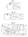
- FIG. 1 Another known device making it possible to avoid these drawbacks, and ensuring timed preheating of the cathodes of the lamp with a view to obtaining an ideal temperature thereof before ignition, is illustrated by the diagram of FIG. 1 attached. It mainly comprises a bimetallic element TC-which provides the desired time delay and which controls a microswitch tc connected in series in the supply circuit of the cathodes of the lamp. This micro-contact is closed at rest.
- the bimetallic element TC supplied by means of an auxiliary winding SL of the ballast inductance BL of the lamp FL, s' heated.
- the FL lamp remains inert, the voltage between the cathodes being insufficient for ignition.
- the cost is established by these cathodes and the micro-contact tc.
- the cathodes heat up, as does the bimetallic element TC.
- this element As soon as the temperature of this element reaches a value predetermined, it switches and controls the opening of the micro-contact tc.
- the overvoltage generated by the interruption of the current in the ballast inductor BL causes the tube to prime.
- Such a device has the disadvantage of requiring a ballast inductor BL provided with an auxiliary winding SL, therefore of a higher cost and a larger volume.
- the cooling time of the bimetallic element TC imposes a minimum duration between two consecutive ignitions.
- the ignition device beats, which in the long term leads to its destruction.
- the present invention therefore relates to an ignition device associated with a ballast inductor of the standard type for corona choke, intended to measure the optimal preheating of the cathodes for a defined time and to control the ignition at a time when the probability of this ignition is maximum.
- the device of the invention is designed so as not to repeat an order not followed by the effective lighting of the lamp, this anomaly can only be due to the failure of an element of the installation, in particular of the lamp.
- the ignition circuit of FIG. 2 comprises, from an alternating current source AC, connected between two inputs E and F of the circuit, the fluorescent lamp FL with its filaments or cathodes Kl and K2, a ballast inductance BL connected between the first end of the cathode Kl and the input E, a suppressor capacitor C6 connected between the second ends of the cathodes Kl and K2, a relay 'LR controlling a contact rl, and a timing and electronic synchronization circuit MN .
- the timing and synchronization circuit MN comprises in particular a first input A connected to the input E of the circuit, a second input B connected to the other input F of the circuit via the cathode K2, and two outputs G and H connected respectively to the terminals of the excitation winding of the relay RL.
- timing and synchronization circuit MN has ordered the ignition of the lamp FL at a time such that the overvoltage causing the ignition of this lamp is optimal, this lamp must light up. If this is not the case, this lamp is defective and there is absolutely no point in the MN circuit undertaking a second operating cycle in order to provide a second ignition command.
- This second cycle can only take place if the supply voltage of the circuit MN is momentarily removed, either following the known reflex of the user operating the general supply switch, or by replacing the defective lamp: as soon as the this is removed, the circuit MN is no longer supplied and it returns to its initial position.
- the installation of a new FL lamp restores the supply of the circuit MN which then supplies the excitation voltage to the relay RL. The operation of the circuit continues as previously described.
- the ignition circuit of FIG. 2 overcomes all thermal constraints (minimum time between two consecutive ignitions imposed by the cooling time of the bimetallic element) of known circuits.
- an electronic timing and synchronization circuit it allows precise preheating of the cathodes which reach at the time of the priming command. an optimal temperature conducive to obtaining a long service life.
- FIG. 3 the detailed diagram of an exemplary embodiment of the ignition circuit of the invention.
- the two inputs A and B of the circuit MN are respectively connected to the input E of the circuit and, via the cathode K2 of the lamp FL to the input F.
- the two outputs G and H of the circuit MN are respectively connected to the ends of the excitation winding of the relay RL.
- the timing and synchronization circuit MN comprises in particular a full-wave rectification circuit RB, one input of which is connected to input A via a capacitor Cl and the other input of which is connected to input B.
- a stabilization diode with Zener effect DZ and a polarized capacitor C2 are connected in parallel between the unreferenced outputs of the rectification circuit RB.
- the circuit MN also includes a monostable circuit NE which can be an integrated circuit of the type sold under the reference 555.
- This monostable includes eight access terminals: terminals 1 and 8 (power supply) are respectively connected to the anode and to the cathode of the Zener diode DZ, terminal 2 (trigger) is connected, on the one hand, to the anode of the Zener diode via a polarized capacitor C3, on the other hand, to the cathode of this diode via an RI resistor; terminal 3 (output) of this monostable is connected to the anode of a protective diode Dl whose cathode is connected to the output H; terminal 4 (reset) is connected to terminal 2; terminal 5 (reference voltage) is connected, via a capacitor C4 to the anode of the Zener diode DZ; terminal 6 (threshold) is connected, on the one hand, to the cathode of this diode via a resistor R2, on the other
- the circuit MN also comprises a protection diode D2 whose anode and cathode are respectively connected between the outputs G and H.
- the monostable NE powered by a voltage Vl supplied between its terminals 1 and 8 after having been triggered by a voltage of amplitude at least equal to one third of the amplitude of the voltage Vl and applied to its terminal 2, switches as soon as the amplitude of the voltage supplied on terminal 6 becomes equal to the amplitude of an internal reference voltage V2.
- the amplitude of this reference voltage defined by a resistance bridge, is equal to 2/3 of the amplitude of the supply voltage Vl.
- An AC supply voltage is supplied to the inputs E and F of the circuit of FIG. 3, therefore also to the inputs of the rectifier bridge RB via the cathode K2 of the lamp FL.
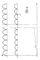
- the capacity of the filtering capacitor C2 connected between the outputs of the rectifier bridge RB is chosen so that this filtering is insufficient and that the rectified voltage supplied at the terminals of this capacitor has a non-negligible undulation, represented by the curve Vl of FIG. 4
- This voltage is supplied between terminals 1 and 8 of the monostable NE which develops an internal reference voltage whose amplitude is equal to 2/3 of the amplitude of this rectified voltage.
- This reference voltage is represented by the curve V2 in Figure 4.
- the capacitor C3 charges through the resistor R1. As soon as qye the potential difference at the terminals of this capacitor is equal to one third of the voltage Vl supplied to the supply terminals 1 and 8 of the monostable NE by the rectifier bridge RB, this monostable is triggered: the internal connection between the terminals 1 and 8 is interrupted and the capacitor C5 can charge through the resistor R2. The variation of the voltage at the terminals of this capacitor is illustrated by the curve VC5 in FIG. 4. Simultaneously, a positive output voltage is supplied on terminal 3, therefore on output H; of the timing and synchronization circuit MN through the protection diode Dl.
- the relay RL normally supplied, is energized and the contact ri goes to the closed position: the current is established by the cathodes K1 and K2 which heat up. The voltage between these cathodes is insufficient to cause ignition and the FL lamp remains inert.
- the voltage VC5 across the capacitor C5 increases: this rise in voltage is slow compared to variations in the reference voltage V2. It follows that the amplitude of the voltage VC5 can only become equal to the amplitude of this reference voltage at an instant AP which coincides practically with a passage of the reference voltage through its minimum.
- the monostable NE switches: no voltage is no longer supplied to terminal 3 and the relay RL which is no longer supplied returns to its resting state; the contact rl goes to the open position thus interrupting the preheating of the cathodes K1 and K2.
- the overvoltage generated by the interruption of the current in the ballast inductor BL causes the FL lamp to strike.
- a new triggering of the NE monostable is then only possible after an interruption of its supply.
- the ignition of the lamp FL was therefore well controlled, at an instant AP having a constant phase shift with the reference voltage V2 therefore with the supply voltage Vl of the monostable NE.
- a capacitor Cl of determined capacity and a relay RL whose response time is known, it is therefore possible to cause the lamp FL to light up at the precise instant when the AC supply voltage AC of this lamp, supplied between points E and F and whose phase shift relative to the supply voltage Vl of the monostable NE is defined by the capacitor Cl, is such that the overvoltage obtained is optimal for the lighting of the lamp. It is therefore the same for the probability of ignition of this lamp.
- the duration of the preheating of the cathodes K1 and K2 is entirely defined by the time constant of the circuit R2-C5. It is therefore easy, while retaining the synchronization of the lamp ignition command, to optimize this preheating.
- the duration of this preheating can be reduced by incorporating a diode in series in the preheating circuit.
- the rectification circuit in bridge RB is unbalanced by the addition of a resistor in the appropriate branch. This resistance, alternating between two in communication with the filtering capacitor makes filtering worse on this alternation.
- the monostable NE then has a preferential trigger on the chosen alternation.
Landscapes
- Circuit Arrangements For Discharge Lamps (AREA)
Applications Claiming Priority (2)
| Application Number | Priority Date | Filing Date | Title |
|---|---|---|---|
| FR8025435A FR2495428A1 (fr) | 1980-12-01 | 1980-12-01 | Circuit d'allumage pour lampe fluorescente |
| FR8025435 | 1980-12-01 |
Publications (1)
| Publication Number | Publication Date |
|---|---|
| EP0053951A1 true EP0053951A1 (fr) | 1982-06-16 |
Family
ID=9248510
Family Applications (1)
| Application Number | Title | Priority Date | Filing Date |
|---|---|---|---|
| EP81401678A Withdrawn EP0053951A1 (fr) | 1980-12-01 | 1981-10-23 | Circuit d'allumage pour lampe fluorescente |
Country Status (2)
| Country | Link |
|---|---|
| EP (1) | EP0053951A1 (OSRAM) |
| FR (1) | FR2495428A1 (OSRAM) |
Citations (2)
| Publication number | Priority date | Publication date | Assignee | Title |
|---|---|---|---|---|
| BE525669A (OSRAM) * | ||||
| US3760224A (en) * | 1971-08-05 | 1973-09-18 | Tokai Rika Co Ltd | Discharge lamp igniting circuit |
-
1980
- 1980-12-01 FR FR8025435A patent/FR2495428A1/fr active Granted
-
1981
- 1981-10-23 EP EP81401678A patent/EP0053951A1/fr not_active Withdrawn
Patent Citations (2)
| Publication number | Priority date | Publication date | Assignee | Title |
|---|---|---|---|---|
| BE525669A (OSRAM) * | ||||
| US3760224A (en) * | 1971-08-05 | 1973-09-18 | Tokai Rika Co Ltd | Discharge lamp igniting circuit |
Also Published As
| Publication number | Publication date |
|---|---|
| FR2495428B3 (OSRAM) | 1983-09-23 |
| FR2495428A1 (fr) | 1982-06-04 |
Similar Documents
| Publication | Publication Date | Title |
|---|---|---|
| EP0288924B1 (fr) | Dispositif d'alimentation d'une lampe à décharge | |
| FR2614166A1 (fr) | Circuit a semi-conducteur pour le fonctionnement d'une lampe a decharge a courant continu | |
| EP0066481A1 (fr) | Dispositif d'alimentation électronique pour lampes à décharge | |
| FR2493092A1 (fr) | Circuit d'amorcage et de commande pour lampes a decharge | |
| FR2493543A1 (fr) | Appareil a lumiere-eclair electrique | |
| EP0008835A1 (fr) | Circuit électrique pour l'allumage d'un détonateur | |
| FR2489070A1 (fr) | Dispositif d'allumage de lampe a decharge | |
| EP0491589A1 (fr) | Générateur d'allumage haute énergie notamment pour turbine à gaz | |
| FR2493091A1 (fr) | Circuit d'amorcage et de commande pour lampes a decharge | |
| WO2005046293A1 (ja) | 高圧放電灯点灯装置及び照明器具 | |
| NO323736B1 (no) | Tenningskrets for en hoytrykks-gassutladningslampe | |
| EP0053951A1 (fr) | Circuit d'allumage pour lampe fluorescente | |
| FR2497051A1 (fr) | Dispositif d'eclairage fluorescent a double niveau d'eclairage | |
| NZ315657A (en) | Process and circuit for striking a high-pressure gas discharge lamp | |
| EP0051537A1 (fr) | Amorceur pour lampe à décharge | |
| US5479075A (en) | Fluorescent lamp starter circuit | |
| EP0978941B1 (fr) | Circuit de production d'arcs électriques | |
| EP0063507B1 (fr) | Starter électronique pour tube fluorescent, comportant un circuit temporisateur coopérant avec un circuit de surtension et un circuit de préchauffage | |
| EP0054443A1 (fr) | Circuit pour l'allumage et la commande graduelle d'une lampe fluorescente | |
| FR2497052A1 (fr) | Dispositif d'eclairage fluorescent a double niveau d'eclairage | |
| EP0026531A1 (fr) | Démarreur pour lampes telles que lampes fluorescentes | |
| WO1987007469A1 (fr) | Systeme electronique d'alimentation pour tubes fluorescents a electrodes | |
| CH644486A5 (en) | Electronic starter for fluorescent lamp | |
| FR2492211A1 (fr) | Appareil generateur de lumiere-eclair electrique | |
| EP0933978A1 (fr) | Dispositif d'amorcage pour l'alimentation de lampes à arc |
Legal Events
| Date | Code | Title | Description |
|---|---|---|---|
| PUAI | Public reference made under article 153(3) epc to a published international application that has entered the european phase |
Free format text: ORIGINAL CODE: 0009012 |
|
| AK | Designated contracting states |
Designated state(s): AT BE CH DE FR GB IT LU NL SE |
|
| 17P | Request for examination filed |
Effective date: 19820922 |
|
| STAA | Information on the status of an ep patent application or granted ep patent |
Free format text: STATUS: THE APPLICATION IS DEEMED TO BE WITHDRAWN |
|
| 18D | Application deemed to be withdrawn |
Effective date: 19840426 |
|
| RIN1 | Information on inventor provided before grant (corrected) |
Inventor name: NORE, MICHEL Inventor name: HESS, JEAN-MARC Inventor name: AUDET, JACQUES DENIS JULIEN |