EP0053533B1 - Verfahren zum Reduzieren des Alterns piezo-elektrischer Resonatoren - Google Patents
Verfahren zum Reduzieren des Alterns piezo-elektrischer Resonatoren Download PDFInfo
- Publication number
- EP0053533B1 EP0053533B1 EP81401804A EP81401804A EP0053533B1 EP 0053533 B1 EP0053533 B1 EP 0053533B1 EP 81401804 A EP81401804 A EP 81401804A EP 81401804 A EP81401804 A EP 81401804A EP 0053533 B1 EP0053533 B1 EP 0053533B1
- Authority
- EP
- European Patent Office
- Prior art keywords
- resonator
- state
- quartz
- crystal
- stabilisation method
- Prior art date
- Legal status (The legal status is an assumption and is not a legal conclusion. Google has not performed a legal analysis and makes no representation as to the accuracy of the status listed.)
- Expired
Links
- 230000032683 aging Effects 0.000 title description 8
- 238000004519 manufacturing process Methods 0.000 title description 2
- VYPSYNLAJGMNEJ-UHFFFAOYSA-N silicon dioxide Inorganic materials O=[Si]=O VYPSYNLAJGMNEJ-UHFFFAOYSA-N 0.000 claims description 29
- 239000010453 quartz Substances 0.000 claims description 22
- 238000000034 method Methods 0.000 claims description 17
- 150000002500 ions Chemical class 0.000 claims description 13
- 230000006641 stabilisation Effects 0.000 claims description 12
- 239000000463 material Substances 0.000 claims description 11
- 230000010355 oscillation Effects 0.000 claims description 9
- 238000002513 implantation Methods 0.000 claims description 5
- 229910052734 helium Inorganic materials 0.000 claims description 4
- 239000001307 helium Substances 0.000 claims description 4
- WHXSMMKQMYFTQS-UHFFFAOYSA-N Lithium Chemical compound [Li] WHXSMMKQMYFTQS-UHFFFAOYSA-N 0.000 claims description 3
- 229910052790 beryllium Inorganic materials 0.000 claims description 3
- ATBAMAFKBVZNFJ-UHFFFAOYSA-N beryllium atom Chemical compound [Be] ATBAMAFKBVZNFJ-UHFFFAOYSA-N 0.000 claims description 3
- SWQJXJOGLNCZEY-UHFFFAOYSA-N helium atom Chemical compound [He] SWQJXJOGLNCZEY-UHFFFAOYSA-N 0.000 claims description 3
- 229910052744 lithium Inorganic materials 0.000 claims description 3
- 230000000087 stabilizing effect Effects 0.000 claims description 3
- WSMQKESQZFQMFW-UHFFFAOYSA-N 5-methyl-pyrazole-3-carboxylic acid Chemical group CC1=CC(C(O)=O)=NN1 WSMQKESQZFQMFW-UHFFFAOYSA-N 0.000 claims description 2
- GQYHUHYESMUTHG-UHFFFAOYSA-N lithium niobate Chemical group [Li+].[O-][Nb](=O)=O GQYHUHYESMUTHG-UHFFFAOYSA-N 0.000 claims description 2
- 230000009466 transformation Effects 0.000 claims description 2
- 238000010884 ion-beam technique Methods 0.000 claims 1
- 238000003303 reheating Methods 0.000 claims 1
- 239000013078 crystal Substances 0.000 description 30
- 239000010410 layer Substances 0.000 description 12
- PEDCQBHIVMGVHV-UHFFFAOYSA-N Glycerine Chemical compound OCC(O)CO PEDCQBHIVMGVHV-UHFFFAOYSA-N 0.000 description 8
- 239000008188 pellet Substances 0.000 description 6
- 238000005468 ion implantation Methods 0.000 description 5
- 238000005299 abrasion Methods 0.000 description 4
- 238000011105 stabilization Methods 0.000 description 4
- 230000004075 alteration Effects 0.000 description 3
- 230000015572 biosynthetic process Effects 0.000 description 3
- 230000008569 process Effects 0.000 description 3
- 206010001488 Aggression Diseases 0.000 description 2
- 230000001133 acceleration Effects 0.000 description 2
- 230000016571 aggressive behavior Effects 0.000 description 2
- 238000004140 cleaning Methods 0.000 description 2
- 230000000052 comparative effect Effects 0.000 description 2
- 238000009792 diffusion process Methods 0.000 description 2
- 230000006872 improvement Effects 0.000 description 2
- 239000012535 impurity Substances 0.000 description 2
- 238000010849 ion bombardment Methods 0.000 description 2
- 238000010002 mechanical finishing Methods 0.000 description 2
- 230000000750 progressive effect Effects 0.000 description 2
- 239000011241 protective layer Substances 0.000 description 2
- 239000000377 silicon dioxide Substances 0.000 description 2
- XLYOFNOQVPJJNP-UHFFFAOYSA-N water Chemical compound O XLYOFNOQVPJJNP-UHFFFAOYSA-N 0.000 description 2
- 239000003082 abrasive agent Substances 0.000 description 1
- 239000002253 acid Substances 0.000 description 1
- 238000004873 anchoring Methods 0.000 description 1
- 238000000137 annealing Methods 0.000 description 1
- 238000000576 coating method Methods 0.000 description 1
- 239000002178 crystalline material Substances 0.000 description 1
- 230000003628 erosive effect Effects 0.000 description 1
- 238000000227 grinding Methods 0.000 description 1
- 238000010438 heat treatment Methods 0.000 description 1
- -1 helium ions Chemical class 0.000 description 1
- 238000003754 machining Methods 0.000 description 1
- 239000011159 matrix material Substances 0.000 description 1
- 239000007769 metal material Substances 0.000 description 1
- 239000002245 particle Substances 0.000 description 1
- 230000000149 penetrating effect Effects 0.000 description 1
- 239000011253 protective coating Substances 0.000 description 1
- 230000009467 reduction Effects 0.000 description 1
- 238000007789 sealing Methods 0.000 description 1
- 239000000126 substance Substances 0.000 description 1
- 239000002344 surface layer Substances 0.000 description 1
- 230000008961 swelling Effects 0.000 description 1
- 238000004017 vitrification Methods 0.000 description 1
- 238000003466 welding Methods 0.000 description 1
Images
Classifications
-
- H—ELECTRICITY
- H03—ELECTRONIC CIRCUITRY
- H03H—IMPEDANCE NETWORKS, e.g. RESONANT CIRCUITS; RESONATORS
- H03H3/00—Apparatus or processes specially adapted for the manufacture of impedance networks, resonating circuits, resonators
- H03H3/007—Apparatus or processes specially adapted for the manufacture of impedance networks, resonating circuits, resonators for the manufacture of electromechanical resonators or networks
- H03H3/02—Apparatus or processes specially adapted for the manufacture of impedance networks, resonating circuits, resonators for the manufacture of electromechanical resonators or networks for the manufacture of piezoelectric or electrostrictive resonators or networks
- H03H3/04—Apparatus or processes specially adapted for the manufacture of impedance networks, resonating circuits, resonators for the manufacture of electromechanical resonators or networks for the manufacture of piezoelectric or electrostrictive resonators or networks for obtaining desired frequency or temperature coefficient
Definitions
- the present invention relates to the field of piezoelectric resonators used in applications where an oscillation frequency must be defined with high stability. This is the case, for example, with pilot oscillators or frequency filters used in radioelectricity and telephony.
- Such resonators are made of a monocrystalline material such as quartz, a variety of crystallized silica, cut in a block of generally parallelepiped shape, and provided with electrodes on two of its opposite faces for the application of the necessary electrical voltages.
- the frequency of a piezoelectric resonator depends on some of its dimensions, and it is adjusted by mechanical grinding operations in the presence of abrasive materials, according to several successive stages, first of roughing and then of finishing.
- the resonator is then provided with its electrodes, most often made up of thin metallic layers deposited on the suitable faces, and, before use, put into operation for a given period, in an electrical assembly for training or “aging”.
- the ion bombardment constitutes an ion implantation step so as to transform the surface of the crystal into a layer of vitreous silica, the energy of the ions (approximately 100 times greater) having the required value to reach precisely this purpose.
- a continuous protective layer is created, made of a material identical to that of the crystal, on the surfaces of the crystal which have been subjected to mechanical finishing operations, this layer consisting of amorphous silica in the case of quartz.
- the fundamental characteristic of the invention is to form this layer directly from the crystalline material of the resonator itself, by a method of implanting selected ions.
- the crystal is thus coated with a vitrified layer which shelters it from the aggressions of the environment, and, moreover, the disturbed zone which was mentioned above is made homogeneous: the vitrification carried out makes disappear the dislocations and superficial crevices. It is further noted that, surprisingly, the treatment does not significantly modify the oscillation frequency.
- the nature of the ions to be implanted can be chosen within a certain range of atomic masses, it is in the field of light ions, such as those of helium, lithium and beryllium that it is particularly advantageous to address, these ions penetrating more easily into the crystal lattice.
- the density of the beam used will vary depending on the type of ions used and the crystal to be treated. In general, it has been found that a density of the order of 1.5 ⁇ 10 16 ions / cm 2 is perfectly suitable.
- the acceleration voltage will in all cases be less than 200 kV and preferably of the order of 100 kV.
- the duration of the treatment is variable according to the value of the above parameters and can preferably vary between a few minutes and several tens of minutes.
- a duration of the order of 10 min is suitable. Those skilled in the art will vary these different parameters so that the amorphous layer obtained after treatment is preferably less than 1 micron. According to a preferred embodiment, it has been found that a thickness of the order of 7,500 Angstroms is suitable. This crystal is then annealed at a temperature below the curie point and preferably of the order of 400 ° C. The duration of the heat treatment will be of the order of approximately one hour.
- the formation of the outer protective layer thus eliminates the causes listed above which are partly responsible for the long aging of a resonator before stabilization.
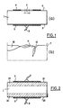
- the invention which is the subject of this patent consists of a method for stabilizing over time a crystalline piezoelectric resonator, consisting of a block (1) of material in the crystalline state, characterized in that it comprises an ion implantation step on some of the faces (21, 22) of this block, ensuring the transformation of the material, up to a determined depth (23, 24) thereof, at the glassy state.
- Figure 1 shows, in two parts (a) and (b), a sectional view of a piezoelectric resonator in quartz crystal after mechanical abrasion for the purpose of finishing.
- (a) is shown the whole of the resonator 1, with two main faces 2 and 3 facing each other, the mutual distance of which contributes to the definition of the resonance frequency. These faces are covered with electrodes 4 and 5, in the form of thin metallic layers, provided with connections such as 6 for the application of the necessary electrical voltages.
- FIG. 2 shows a sectional view of a piezoelectric resonator in quartz crystal, after finishing by mechanical abrasion, but having undergone the stabilization process over time according to the invention.
- This process which consists of ion implantation of light ions such as those of helium, lithium or beryllium, on the two faces 21 and 22 facing each other, determines the formation of surface layers of silica amorphous 23 and 24, which corresponds to the state of matter known as "glassy".
- This continuous layer created at the expense of surface alterations of the resonator, eliminates these and protects the crystalline quartz from external aggressions, with the advantageous consequences indicated above; moreover, its mode of formation from quartz itself ensures its attachment or "perfect anchoring on the crystal.
- this same training mode guarantees that it does not disturb the oscillation / overvoltage characteristics of the resonator, which cannot be completely guaranteed by the heterogeneous layers deposited on the main faces. In addition, this amorphous layer comes from the crystal itself and therefore does not cause excess thickness.
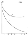
- the resonators having undergone this treatment are subjected to aging in an enclosure thermostatically controlled at 70 ° C.
- a group of identical but untreated resonators is subjected to the same aging, mounted in the same way in identical housings.
- FIG. 3 represents the relative variations in frequency IlF / F of the quartz pellet as a function of time.
- the curve (1) relates to a crystal treated according to the example above, the curve (2) being relative to a crystal of the same origin, but not treated.
- the slope of the curve becomes very low after approximately three months whereas for untreated crystals, this slope does not weaken until after approximately eight months of aging.
- the slope of the curve relating to untreated crystals always remains of the order of 3 to 4 times greater than that of the curve relating to treated crystals, even after a year or more.
Landscapes
- Engineering & Computer Science (AREA)
- Manufacturing & Machinery (AREA)
- Piezo-Electric Or Mechanical Vibrators, Or Delay Or Filter Circuits (AREA)
Claims (8)
Applications Claiming Priority (2)
| Application Number | Priority Date | Filing Date | Title |
|---|---|---|---|
| FR8024803 | 1980-11-21 | ||
| FR8024803A FR2494931B1 (fr) | 1980-11-21 | 1980-11-21 | Procede de stabilisation dans le temps d'un resonateur piezo-electrique |
Publications (2)
| Publication Number | Publication Date |
|---|---|
| EP0053533A1 EP0053533A1 (de) | 1982-06-09 |
| EP0053533B1 true EP0053533B1 (de) | 1984-02-29 |
Family
ID=9248250
Family Applications (1)
| Application Number | Title | Priority Date | Filing Date |
|---|---|---|---|
| EP81401804A Expired EP0053533B1 (de) | 1980-11-21 | 1981-11-17 | Verfahren zum Reduzieren des Alterns piezo-elektrischer Resonatoren |
Country Status (5)
| Country | Link |
|---|---|
| US (1) | US4397884A (de) |
| EP (1) | EP0053533B1 (de) |
| JP (1) | JPS57112122A (de) |
| DE (1) | DE3162446D1 (de) |
| FR (1) | FR2494931B1 (de) |
Families Citing this family (2)
| Publication number | Priority date | Publication date | Assignee | Title |
|---|---|---|---|---|
| GB8310298D0 (en) * | 1983-04-15 | 1983-05-18 | Atomic Energy Authority Uk | Modification of surface properties of ceramics |
| RU2150172C1 (ru) * | 1998-05-28 | 2000-05-27 | Омский государственный технический университет | Способ изготовления кристаллических элементов |
Family Cites Families (2)
| Publication number | Priority date | Publication date | Assignee | Title |
|---|---|---|---|---|
| US2989799A (en) * | 1958-10-15 | 1961-06-27 | Bell Telephone Labor Inc | Stabilization of quartz crystal frequency controlling elements |
| US3914836A (en) * | 1974-06-21 | 1975-10-28 | Us Army | Method for processing quartz crystal resonators |
-
1980
- 1980-11-21 FR FR8024803A patent/FR2494931B1/fr not_active Expired
-
1981
- 1981-11-17 DE DE8181401804T patent/DE3162446D1/de not_active Expired
- 1981-11-17 EP EP81401804A patent/EP0053533B1/de not_active Expired
- 1981-11-19 US US06/323,075 patent/US4397884A/en not_active Expired - Fee Related
- 1981-11-19 JP JP56186088A patent/JPS57112122A/ja active Pending
Also Published As
| Publication number | Publication date |
|---|---|
| FR2494931B1 (fr) | 1988-01-08 |
| FR2494931A1 (fr) | 1982-05-28 |
| DE3162446D1 (en) | 1984-04-05 |
| EP0053533A1 (de) | 1982-06-09 |
| JPS57112122A (en) | 1982-07-13 |
| US4397884A (en) | 1983-08-09 |
Similar Documents
| Publication | Publication Date | Title |
|---|---|---|
| EP3706180B1 (de) | Verfahren zur herstellung eines mikroelektromechanischen systems, das aus einer abgeschiedenen piezoelektrischen oder ferroelektrischen schicht hergestellt wird | |
| KR100438467B1 (ko) | 박막 공진기 장치 및 이의 제조 방법 | |
| FR2962598A1 (fr) | Procede d'implantation d'un materiau piezoelectrique | |
| EP2341617B1 (de) | Akustischer Resonator, der ein Elektret umfasst, sowie Herstellungsverfahren dieses Resonators und Anwendung auf gekoppelte Resonatoren bei umschaltbaren Filtern | |
| KR20190031228A (ko) | 탄성 표면파 디바이스용 복합 기판의 제조 방법 | |
| WO2017109005A1 (fr) | Procede de fabrication d'une couche piezoelectrique monocristalline et dispositif microelectronique, photonique ou optique comprenant une telle couche | |
| FR3045677A1 (fr) | Procede de fabrication d'une couche monocristalline, notamment piezoelectrique | |
| WO2017207911A1 (fr) | Structure hybride pour dispositif a ondes acoustiques de surface | |
| FR2914492A1 (fr) | Procede de fabrication de structures avec couches ferroelectriques reportees. | |
| WO2024115410A1 (fr) | Support comprenant une couche de piegeage de charges, substrat composite comprenant un tel support et procedes de fabrication associes. | |
| WO2024115411A1 (fr) | Support comprenant une couche de piegeage de charges, substrat composite comprenant un tel support et procedes de fabrication associes | |
| EP0053533B1 (de) | Verfahren zum Reduzieren des Alterns piezo-elektrischer Resonatoren | |
| WO2024115414A1 (fr) | Support comprenant une couche de piegeage de charges, substrat composite comprenant un tel support et procedes de fabrication associes | |
| EP4144897B1 (de) | Verfahren zur herstellung eines verbundsubstrats und verbundsubstrat | |
| EP3766094B1 (de) | Verfahren zur herstellung einer dünnschicht aus einem ferroelektrikum auf alkalibasis | |
| FR2684835A1 (fr) | Dispositif resonateur piezoelectrique a quartz. | |
| EP4562982A1 (de) | Verfahren zur herstellung einer eindomänen-dünnschicht aus lithiumhaltigem ferroelektrischem material | |
| CN114214732B (zh) | 一种改善复合薄膜表面极化反转现象的方法及复合薄膜 | |
| EP3465788B1 (de) | Verfahren zur herstellung einer schicht | |
| EP3465787A1 (de) | Verfahren zur reparatur von defekten in einer schicht durch implantation und dann ablösung von einem substrat | |
| FR2580864A1 (fr) | Couche barriere au bombardement ionique pour tube a vide | |
| FR3141308A1 (fr) | Procede de fabrication d’une couche piezoelectrique sur un substrat | |
| EP4559018A1 (de) | Verfahren zur herstellung eines trägersubstrats für eine hochfrequenzanwendung | |
| FR3138240A1 (fr) | Procédé de fabrication d’un substrat support pour application radiofréquences | |
| FR2799589A1 (fr) | Procede de fabrication d'un dispositif a ondes acoustiques de surface |
Legal Events
| Date | Code | Title | Description |
|---|---|---|---|
| PUAI | Public reference made under article 153(3) epc to a published international application that has entered the european phase |
Free format text: ORIGINAL CODE: 0009012 |
|
| AK | Designated contracting states |
Designated state(s): CH DE GB IT LI NL |
|
| 17P | Request for examination filed |
Effective date: 19820809 |
|
| RAP1 | Party data changed (applicant data changed or rights of an application transferred) |
Owner name: COMPAGNIE D'ELECTRONIQUE ET DE PIEZO-ELECTRICITE - |
|
| ITF | It: translation for a ep patent filed | ||
| GRAA | (expected) grant |
Free format text: ORIGINAL CODE: 0009210 |
|
| AK | Designated contracting states |
Designated state(s): CH DE GB IT LI NL |
|
| REF | Corresponds to: |
Ref document number: 3162446 Country of ref document: DE Date of ref document: 19840405 |
|
| PGFP | Annual fee paid to national office [announced via postgrant information from national office to epo] |
Ref country code: DE Payment date: 19841022 Year of fee payment: 4 Ref country code: CH Payment date: 19841022 Year of fee payment: 4 |
|
| PLBE | No opposition filed within time limit |
Free format text: ORIGINAL CODE: 0009261 |
|
| STAA | Information on the status of an ep patent application or granted ep patent |
Free format text: STATUS: NO OPPOSITION FILED WITHIN TIME LIMIT |
|
| 26N | No opposition filed | ||
| PGFP | Annual fee paid to national office [announced via postgrant information from national office to epo] |
Ref country code: NL Payment date: 19851130 Year of fee payment: 5 |
|
| PG25 | Lapsed in a contracting state [announced via postgrant information from national office to epo] |
Ref country code: LI Effective date: 19861130 Ref country code: CH Effective date: 19861130 |
|
| PG25 | Lapsed in a contracting state [announced via postgrant information from national office to epo] |
Ref country code: NL Effective date: 19870601 |
|
| NLV4 | Nl: lapsed or anulled due to non-payment of the annual fee | ||
| GBPC | Gb: european patent ceased through non-payment of renewal fee | ||
| REG | Reference to a national code |
Ref country code: CH Ref legal event code: PL |
|
| PG25 | Lapsed in a contracting state [announced via postgrant information from national office to epo] |
Ref country code: DE Effective date: 19870801 |
|
| PG25 | Lapsed in a contracting state [announced via postgrant information from national office to epo] |
Ref country code: GB Effective date: 19881118 |