EP0053075A2 - Nichtflüchtiger Speicher - Google Patents
Nichtflüchtiger Speicher Download PDFInfo
- Publication number
- EP0053075A2 EP0053075A2 EP81401837A EP81401837A EP0053075A2 EP 0053075 A2 EP0053075 A2 EP 0053075A2 EP 81401837 A EP81401837 A EP 81401837A EP 81401837 A EP81401837 A EP 81401837A EP 0053075 A2 EP0053075 A2 EP 0053075A2
- Authority
- EP
- European Patent Office
- Prior art keywords
- transistor
- line
- transistors
- selecting
- write
- Prior art date
- Legal status (The legal status is an assumption and is not a legal conclusion. Google has not performed a legal analysis and makes no representation as to the accuracy of the status listed.)
- Granted
Links
Images


Classifications
-
- G—PHYSICS
- G11—INFORMATION STORAGE
- G11C—STATIC STORES
- G11C16/00—Erasable programmable read-only memories
- G11C16/02—Erasable programmable read-only memories electrically programmable
- G11C16/04—Erasable programmable read-only memories electrically programmable using variable threshold transistors, e.g. FAMOS
- G11C16/0408—Erasable programmable read-only memories electrically programmable using variable threshold transistors, e.g. FAMOS comprising cells containing floating gate transistors
- G11C16/0441—Erasable programmable read-only memories electrically programmable using variable threshold transistors, e.g. FAMOS comprising cells containing floating gate transistors comprising cells containing multiple floating gate devices, e.g. separate read-and-write FAMOS transistors with connected floating gates
-
- H—ELECTRICITY
- H10—SEMICONDUCTOR DEVICES; ELECTRIC SOLID-STATE DEVICES NOT OTHERWISE PROVIDED FOR
- H10B—ELECTRONIC MEMORY DEVICES
- H10B69/00—Erasable-and-programmable ROM [EPROM] devices not provided for in groups H10B41/00 - H10B63/00, e.g. ultraviolet erasable-and-programmable ROM [UVEPROM] devices
Definitions
- the present invention relates to a nonvolatile memory, and more particularly relates to a nonvolatile semiconductor EE-PROM (Electrically Erasable - Programmable Read - Only Memory).
- EE-PROM Electrically Erasable - Programmable Read - Only Memory
- a programmable ROM is widely utilized in, for example, a computer-aided data processing system.
- a ROM can be programmed only once, either at the factory or in the field, by electrically fusing or otherwise removing unwanted internal links. Accordingly, the conventional programmable ROM has a defect in that a mistake in the programming cannot be corrected.
- an EPROM Erasable Programmable ROM
- the stored data can be erased by ultraviolet light and each bit can be electrically reprogrammed with appropriate voltage pulses.
- ultraviolet light since ultraviolet light is required for reprogramming the stored data, it is not easy for an operator to freely reprogram the stored data.
- EE-PROM In recent years, a nonvolatile EE-PROM has been proposed, for example, in the publication "Electronics", February 28, 1980 pages 113 through 117, entitled “16-K EE-PROM relies on tunneling for byte-erasable program storage".
- the EE-PROM is basically comprised of a transistor having a source, a drain, a floating gate and a control gate, in which the floating gate partially includes an area of a very thin insulation layer on the order of a 0 hundred A.
- a tunnel effect can be created, via the thin insulation, between the drain and the floating gate, and thereby data, to be stored in each memory cell, is reprogrammed.
- the EE-PROM is very. useful for an operator in, for example, the computer-aided data processing system, because, as previously mentioned, he can freely reprogram the stored data without using ultraviolet light.
- an EE-PROM circuit of the prior art has the following two defects. Firstly, undesired erasure of data often occurs in some of the half-selected memory cells, which will be explained in detail hereinafter. Secondly, it is not relatively easy during mass-production to produce the EE-PROM circuit devices.
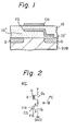
- Fig. 1 illustrates a cross-sectional view showing a known EE-PROM of a prior art.
- a basic transistor especially, an FET (Field Effect Transistor) of the EE-PROM is formed in and on a semiconductor substrate SUB.
- a source S and a drain D of the transistor is formed therein.
- a floating gate FG and a control gate CG are formed via an insulation layer (SiO 2 ) IS.
- the floating gate FG partially faces the substrate, especially the drain D, via a very thin insulation layer IS'.
- the floating gate FG cooperating with the thin insulation layer IS', is necessary to construct the electrically erasable (EE) memory.
- EE electrically erasable
- the voltage level of the floating gate FG is also increased by the positive high voltage, due to the presence of a capacitor formed between the gate CG and the gate FG having a relatively thick insulation layer IS".
- the voltage level, to be applied to the drain D is set at 0 V, an extremely high electric field is created, across the thin insulation layer IS', between the gate FG and the drain D. Then electron charges are injected from the drain D into the floating gate FG, which phenomena provide a tunnel effect. Thereby an erase operation is completed.
- the voltage level of the control gate CG is set at 0 V and the voltage level of the drain D is set at a positive high voltage, and thus the electron charges are injected from the floating gate FG into the drain D.
- Fig. 2 depicts a circuit diagram of a conventional memory cell including the transistor of Fig. 1 therein.
- the memory cell MC of Fig. 2 is fabricated as a two-transistor cell type memory cell.
- the memory cell MC is comprised of a programming transistor Q 1 and a selecting transistor Q 2 which corresponds to the transistor of Fig. 1.
- the symbols D, S, FG and CG denote respectively the aforesaid drain, source, floating gate and control gate.
- the selecting transistor Q 2 is used for accessing the transistor Q 1 when this memory cell MC is specified by an address signal.
- the programming transistor Q 1 functions to store, read and write data alternately.
- transistors Q 1 and Q 2 are connected in series with each other along a column line Y, namely a bit line, and to a ground GND.
- the gate G of the transistor Q 2 is connected to a row line X, namely a word line.
- the control gate' CG of the transistor Q I is connected to a program line PR which is arranged in parallel with the row line X.
- Fig. 3 depicts a circuit diagram of a conventional memory comprised of memory cells MC shown in Fig. 2.
- the members having identical reference symbols are substantially the same as those of Fig. 2.
- a write operation is achieved as follows. If the memory cell MC a is accessed, the positive high voltage, such as +18 V, is applied to the column line Y a and simultaneously the positive high voltage, such as +20 V is applied to the row line X a and thereby the selecting transistor Q 2 of the specified memory cell MC a is turned to ON. At the same time, the positive high voltage is applied to the drain D of the transistor Q 1 and zero voltage is applied to the control gate CG.
- the positive high voltage such as +18 V
- half-selected memory cells such as MC b , MC c and so on, and non-selected memory cells, such as MC d and so on, exist at the same time, other than selected memory cell MC a .
- the half-selected memory cell is defined as follows. That is, the corresponding column line Y is selected, but, the corresponding row line X is not selected, alternately, the corresponding row line X is selected, but, the corresponding column line Y is not selected. When both column and row lines are not selected, the non-selected memory cell is obtained.
- the above-mentioned problem may often occur in the half-selected memory cells, especially the half-selected memory cells defined by the row line X and the remaining column lines other than the column line Y , which memory cell corresponds to the memory cells (MCs) arranged along the row line X a shown in Fig. 3.
- the half-selected memory cells not only the word line X a but also the program line PR a are selected. Therefore, the corresponding transistors Q 2 of the half-selected memory cells are turned ON.
- the above-mentioned undesired erasing may be protected by employing an additional transistor which acts to disconnect the source S from the ground GND, selectively.
- this idea for employing such additional transistor is not perfect in protecting all the undesired erasing.
- the important matter is to pay attention to the existence of a parasitic capacitor formed between the drain D and the substrate SUB (refer to the parasitic capacitor PC shown in Fig. 2). To make the matter worse, the capacitance value of the capacitor PC is considerably large.
- the capacitance value of the capacitor PC may further be increased, because a parasitic capacitor, formed between the substrate SUB and the source S, is also added to the parasitic capacitor PC of the drain D.
- the drain D Since the drain D is provided with a large parasitic capacitor, the voltage level at the drain D cannot change at high speed. Accordingly, the voltage level at the drain D cannot increase at high speed when the positive high voltage V H is applied to the control gate CG. In other words, although the voltage level at the gate CG and also the gate FG changes sharply, the voltage level at the drain D cannot change so sharply. Therefore, a condition, corresponding to the erase operation, is unnecessarily satisfied in a moment during the term in which the voltage level at the drain D follows toward the positive high voltage level at the gate CG and saturates the corresponding positive high'voltage level. Although such undesired erasing occurs in a very short time, if such undesired erasing occurs many times repeatedly, the stored data will completely be erased from the floating gate FG, which is one of the previously mentioned defects of the prior art.
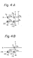
- Fig. 4A depicts an equivalent circuit diagram of each memory cell MC according to the present invention
- Fig. 4B depicts an equivalent circuit diagram of each memory cell MC of the prior art.
- each programming transistor Q 1 of Figs. 2 and 3 is depicted as a single transistor element, in the actual arrangement of the programming transistors Q 1 ; each of the transistors Q 1 is divided into a first transistor Q 11 , acting as a read transistor, having the thick insulation layer IS" and a second transistor Q12 , acting as a write-erase transistor, having a partially thin insulation layer IS'.
- the selecting transistor Q 2 of Fig. 2 or 3 is also divided into a first selecting transistor Q 21 which is connected in series with the read transis- tor Q 11 , as usual, and a second selecting transistor Q 22 which is connected in series with the write-erase transis- to r Q 12 .
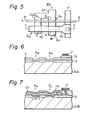
- Fig. 5 illustrates a plan view of a memory cell having the circuit diagram of Fig. 4A, according to the present invention.
- the members having the same reference symbols are identical to those of Fig. 4A.
- the reference symbol DF denotes a diffusion area.
- Fig. 6 is a cross-sectional view of the memory cell shown in Fig. 5 taken along the line 6-6.
- Fig. 7 is a cross-sectional view of the memory cell shown in Fig. 5 taken along the line 7-7.
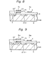
- F ig. 8 is a cross-sectional view of the memory cell shown in Fig. 5 taken along the line 8-8.
- Fig. 9 is a cross-sectional view of the memory cell shown in Fig. 5 taken along the line 9-9.
- the programming transistor Q of Fig. 3 is divided into the read transistor Q11 and the write-erase transistor Q 12 .
- the selecting transistor Q 2 of Fig. 3 is also divided into the first selecting transistor Q21 and the second selecting transistor Q22.
- the diffusion area DF contains n -type impurities therein (see Figs. 8 and 9).
- the diffusion area DF is electrically connected to the column line Y (see Fig. 5).
- the diffusion area DF is formed to be a U-shaped area, as seen from Fig. 5.
- the two gates X and CG traverse across and over the diffusion area DF so as to form four transistors Q 11 ⁇ Q 22 at respective cross portions.
- channels are created at respective transistors Q 11 ⁇ Q22.
- an n-type depletion region is formed.
- the drain D of the transistor Q12 is shorted with the source S of the transistor Q 22 , as seen from the area D(S) of Fig. 9.
- the floating gate FG of the transistor Q12 is provided with a relatively thin insulation layer IS' thereunder, but, other floating gates are provided with the relatively thick insulation layer IS", as seen from Figs. 8 and 9. This insulation layer IS' is thin enough to create the tunnel effect.
- the impurity density of the substrate, located under the floating gate FG may not be the same as that of the drain D thereof, alternately, that impurity density may be a value which enables creation of a full depletion state of this transistor, even though electron charges are fully injected into that gate FG.
- Fig. 10 illustrates a memory circuit diagram comprised of many memory cells according to the present invention shown in Figs.
- Fig. 10 only two column lines are illustrated as Y and Y n , only two row lines are illustrated as X i and X j , only two program lines are illustrated as Y' m and Y' n and only four memory cells are illustrated as MC im , MC in , MC jm and MC.. Further it should be understood that, in each memory cell ( M C), the locations of'the transistors (Q 22 ' Q 12 ) and (Q 21 , Q 11 ) are reversed with respect to the locations thereof shown in Fig. 5, so as to simplify the illustration of the wiring diagram of Fig. 10.
- the corresponding program lines Y' n and so on are not selected, and accordingly the corresponding control gates CG are left in an open state or zero voltage state, in which no undesired erase operation can be expected to occur.
- the control gates CG of these half-selected memory cells receive the positive high voltage V H , however, the write-erase transistors Q12 are left in floating state, and accordingly no undesired erase operation can be performed.
- the write-erase transistor Q 12 is fabricated in a small size, and therefore, the parasitic capacitor (refer to PC in Fig.
- Fig. 10 when the read operation is achieved, the positive voltage is applied to both the row and column lines X, Y of the selected memory cell MC. If the selected memory cell MC stores the logic "1" (no electron charges are held at the floating gate FG thereof), the voltage level of the floating gate is positive, and therefore the threshold level of the selected transistor Q 11 is reduced. Thus, the transistor Q11 is left in the normal - ON state. In this case, current flows from the column line Y to the ground GND via the transistors Q21 and Q 11 , which are now ON.
- the selected memory cell MC stores the logic "0" (electron charges are held at the floating gate FG thereof), the voltage level of the floating gate FG is negative, and therefore the threshold level of the selected transistor Q 11 is increased. Thus, the transistor Q 11 is left in normal - OFF state. In this case, no current flows from the column line Y to the ground GND via the transistors Q 21 and Q 11'
- the stored data "1" or “0” is read from each memory cell.
- the voltage level at the control gate CG is not restricted to the above-mentioned zero voltage, but, may be a suitable positive voltage level which is predetermined, for an erase operation and a write operation, according to the respective threshold levels of the memory cells.
- the following table I shows the voltage level developed at the row line X, the program line Y' and the column line Y, to be supplied in each of the read (READ), the write (WRITE), the partial-erase (PARTIAL ERASE) and the whole-erase (WHOLE ERASE) operations, with respect to the selected memory cell MC s , the half-selected memory cell MC HSX having selected row line X only, the half-selected memory cell MC HSY having the selected column line Y only and the non-selected memory cell MC non
- the reference symbol V 1 denotes the positive high voltage higher than the ordinary power supply voltage level of V CC ; the reference symbol V 2 lenotes a read voltage level at the line Y'; V 3 a read voltage level at the line Y; and, V 4 a suitable read voltage level at the row line X.
- the memory circuit device of the present invention is easy for producing in mass-production. This is because, if slight locational error occurs in the location, with respect to the diffusion area DF of the row line X, the.control gate CG or the floating gate FG, in vertical and/or horizontal directions in the drawing of Fig. 5, such locational error does not cause a significant defect in manufactured memory cells, due to the presence of the U-shaped diffusion area DF.
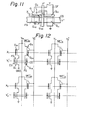
- Fig. 11 illustrates a plan view showing the other embodiment of the memory cell according to the present invention.
- This figure corresponds to Fig. 5 showing the first embodiment according to the present invention.
- the members referenced by the same reference symbols as those of F ig. 5 are substantially the same. Therefore, a third selecting transistor Q 3 and an additional program line Y" are newly introduced therein.
- the third selecting transistor Q 3 cooperates with the second selecting transistor Q 22 .
- the previously mentioned program line PR (Fig. 2) is composed of the first program line Y' and the second program line Y".
- the second program line Y" is coupled to the gate G of the third selecting transistor Q 3 .
- the channel of the transistor Q is also formed inside the U-shaped diffusion area DF.
- the first program line Y' is arranged in parallel with the row line X.
- the second program line Y" is arranged in parallel with the column line Y.
- the line Y" is selected by means of the decoder circuit, usually used for selecting a desired one of the column lines Y.
- Fig. 12 illustrates a memory circuit diagram comprised of many memory cells of another embodiment according to the present invention.
- Y m and Y n only two row lines are illus- trated as X . and X .
- first program lines are illustrated as Y' i and Y' j
- second program lines are illustrated as Y" m and Y"
- only four memory cells are illustrated as MC' im , MC' in MC'.
- the partial-erase operation When the partial-erase operation is commenced, a similar condition of the above whole-erase operation is satisfied with respect only to the selected memory cell, for example MC' im .
- the second program line Y" n is also non-selected, and accordingly the transistor Q 3 is turned to OFF, and the transistor Q 12 of the cell MC' in becomes a floating state. Consequently, the voltage level of the drain D of this transistor Q 12 changes together with the voltage level of the control gate CG and also the floating gate F G of the transistor Q12 in the cell MC' in . Thereby, no undesired erase operation can be expected to occur in the half-selected memory cell MC' in .
- the read operation of the memory shown in Fig. 12 is substantially the same as that of Fig. 10.
- the first program lines Y'. , Y' j Vietnamese of Fig. 12 should be supposed to be the program lines Y' m , Y' n Vietnamese of Fig. 10.
- the second program line Y" m , Y" n Vietnamese of Fig. 12 can be in free states during the read operation, that is the voltage level of these lines Y" m , Y" n may be a high voltage or a low voltage level.
- operations of the memory shown in Fig. 12 are classified as represented by the following Table II. Table II corresponds to the previously cited Table I.
Landscapes
- Engineering & Computer Science (AREA)
- Microelectronics & Electronic Packaging (AREA)
- Non-Volatile Memory (AREA)
- Read Only Memory (AREA)
Applications Claiming Priority (4)
| Application Number | Priority Date | Filing Date | Title |
|---|---|---|---|
| JP166354/80 | 1980-11-26 | ||
| JP55166355A JPS6034198B2 (ja) | 1980-11-26 | 1980-11-26 | 不揮発性メモリ |
| JP166355/80 | 1980-11-26 | ||
| JP55166354A JPS6034197B2 (ja) | 1980-11-26 | 1980-11-26 | 不揮発性メモリ |
Publications (3)
| Publication Number | Publication Date |
|---|---|
| EP0053075A2 true EP0053075A2 (de) | 1982-06-02 |
| EP0053075A3 EP0053075A3 (en) | 1983-11-16 |
| EP0053075B1 EP0053075B1 (de) | 1988-04-20 |
Family
ID=26490755
Family Applications (1)
| Application Number | Title | Priority Date | Filing Date |
|---|---|---|---|
| EP81401837A Expired EP0053075B1 (de) | 1980-11-26 | 1981-11-20 | Nichtflüchtiger Speicher |
Country Status (3)
| Country | Link |
|---|---|
| EP (1) | EP0053075B1 (de) |
| DE (1) | DE3176713D1 (de) |
| IE (1) | IE53867B1 (de) |
Cited By (5)
| Publication number | Priority date | Publication date | Assignee | Title |
|---|---|---|---|---|
| EP0160720A1 (de) * | 1984-05-07 | 1985-11-13 | Deutsche ITT Industries GmbH | Halbleiterspeicherzelle mit einem potentialmässig schwebenden Speichergate |
| EP0085550A3 (en) * | 1982-01-29 | 1986-02-12 | Seeq Technology, Incorporated | Electrically-programmable and electrically-erasable mos memory device |
| EP0284724A3 (en) * | 1987-01-31 | 1989-03-08 | Kabushiki Kaisha Toshiba | Nonvolatile semiconductor memory device |
| EP0570257A1 (de) * | 1992-05-15 | 1993-11-18 | Thomson-Csf | Feldeffekt-Halbleiteranordnung mit sekundärem Gate, Verfahren zur Herstellung und Verwendung in einer Matrix-Ansteuerungsanordnung |
| EP0778581A3 (de) * | 1995-12-07 | 1998-10-14 | Samsung Electronics Co., Ltd. | Nichtflüchtige Speicheranordnung |
Family Cites Families (4)
| Publication number | Priority date | Publication date | Assignee | Title |
|---|---|---|---|---|
| JPS608558B2 (ja) * | 1977-03-23 | 1985-03-04 | 日本電気株式会社 | 読出し専用記憶装置 |
| US4099196A (en) * | 1977-06-29 | 1978-07-04 | Intel Corporation | Triple layer polysilicon cell |
| DE2743422A1 (de) * | 1977-09-27 | 1979-03-29 | Siemens Ag | Wortweise loeschbarer, nicht fluechtiger speicher in floating-gate-technik |
| US4203158A (en) * | 1978-02-24 | 1980-05-13 | Intel Corporation | Electrically programmable and erasable MOS floating gate memory device employing tunneling and method of fabricating same |
-
1981
- 1981-11-20 DE DE8181401837T patent/DE3176713D1/de not_active Expired
- 1981-11-20 EP EP81401837A patent/EP0053075B1/de not_active Expired
- 1981-11-25 IE IE2759/81A patent/IE53867B1/en not_active IP Right Cessation
Cited By (7)
| Publication number | Priority date | Publication date | Assignee | Title |
|---|---|---|---|---|
| EP0085550A3 (en) * | 1982-01-29 | 1986-02-12 | Seeq Technology, Incorporated | Electrically-programmable and electrically-erasable mos memory device |
| EP0160720A1 (de) * | 1984-05-07 | 1985-11-13 | Deutsche ITT Industries GmbH | Halbleiterspeicherzelle mit einem potentialmässig schwebenden Speichergate |
| EP0284724A3 (en) * | 1987-01-31 | 1989-03-08 | Kabushiki Kaisha Toshiba | Nonvolatile semiconductor memory device |
| US4870615A (en) * | 1987-01-31 | 1989-09-26 | Kabushiki Kaisha Toshiba | Nonvolatile floating gate semiconductor memory device |
| EP0440265A3 (de) * | 1987-01-31 | 1991-08-21 | Kabushiki Kaisha Toshiba | Halbleiterfestwertspeichereinrichtung |
| EP0570257A1 (de) * | 1992-05-15 | 1993-11-18 | Thomson-Csf | Feldeffekt-Halbleiteranordnung mit sekundärem Gate, Verfahren zur Herstellung und Verwendung in einer Matrix-Ansteuerungsanordnung |
| EP0778581A3 (de) * | 1995-12-07 | 1998-10-14 | Samsung Electronics Co., Ltd. | Nichtflüchtige Speicheranordnung |
Also Published As
| Publication number | Publication date |
|---|---|
| IE53867B1 (en) | 1989-03-29 |
| IE812759L (en) | 1982-05-26 |
| EP0053075B1 (de) | 1988-04-20 |
| DE3176713D1 (en) | 1988-05-26 |
| EP0053075A3 (en) | 1983-11-16 |
Similar Documents
| Publication | Publication Date | Title |
|---|---|---|
| US4402064A (en) | Nonvolatile memory | |
| US5185718A (en) | Memory array architecture for flash memory | |
| US5245570A (en) | Floating gate non-volatile memory blocks and select transistors | |
| US4377857A (en) | Electrically erasable programmable read-only memory | |
| US6380636B1 (en) | Nonvolatile semiconductor memory device having an array structure suitable to high-density integrationization | |
| EP0247875B1 (de) | Blockmässig elektrisch löschbarer Speicher | |
| US6031765A (en) | Reversed split-gate cell array | |
| US4514830A (en) | Defect-remediable semiconductor integrated circuit memory and spare substitution method in the same | |
| US4375087A (en) | Electrically erasable programmable read only memory | |
| KR100187196B1 (ko) | 불휘발성 반도체 메모리 장치 | |
| US20070206416A1 (en) | Nonvolatile semiconductor memory device | |
| EP0463580A2 (de) | Nichtflüchtige Halbleiterspeicheranordnung | |
| KR960016106B1 (ko) | 비 휘발성 반도체 메모리 장치 | |
| JPH03155667A (ja) | フラッシュ消去epromメモリ用の新規なアーキテクチャー | |
| KR20020042749A (ko) | 불휘발성 반도체 메모리 장치 | |
| EP0637035B1 (de) | Schaltungsstruktur für Speichermatrix und entsprechende Herstellungsverfahren | |
| US4766473A (en) | Single transistor cell for electrically-erasable programmable read-only memory and array thereof | |
| US5572464A (en) | Semiconductor memory device and method of using the same | |
| JP2002528840A (ja) | 不揮発性メモリ素子およびそれを使用する記憶装置におけるプログラム障害をなくすビット線バイアス方法 | |
| EP1214715B1 (de) | 1 transistorzelle für eeprom anwendung | |
| US4379343A (en) | Electrically erasable programmable read-only memory cell having a shared diffusion | |
| EP0053075B1 (de) | Nichtflüchtiger Speicher | |
| US6011717A (en) | EEPROM memory programmable and erasable by Fowler-Nordheim effect | |
| US5398202A (en) | Reprogrammable nonvolatile semiconductor memory formed of MOS transistors and reprogramming method thereof | |
| EP0466051B1 (de) | Programmierbarer nichtflüchtiger Festwertspeicher mit Speicherzellen, jeder mit einem Speichertransistor und einem parallel gekoppelten Schalttransistor und Verfahren zur Speicherung eines Datenbit |
Legal Events
| Date | Code | Title | Description |
|---|---|---|---|
| PUAI | Public reference made under article 153(3) epc to a published international application that has entered the european phase |
Free format text: ORIGINAL CODE: 0009012 |
|
| AK | Designated contracting states |
Designated state(s): DE FR GB NL |
|
| PUAL | Search report despatched |
Free format text: ORIGINAL CODE: 0009013 |
|
| AK | Designated contracting states |
Designated state(s): DE FR GB NL |
|
| 17P | Request for examination filed |
Effective date: 19831203 |
|
| GRAA | (expected) grant |
Free format text: ORIGINAL CODE: 0009210 |
|
| AK | Designated contracting states |
Kind code of ref document: B1 Designated state(s): DE FR GB NL |
|
| PG25 | Lapsed in a contracting state [announced via postgrant information from national office to epo] |
Ref country code: NL Effective date: 19880420 |
|
| REF | Corresponds to: |
Ref document number: 3176713 Country of ref document: DE Date of ref document: 19880526 |
|
| ET | Fr: translation filed | ||
| NLV1 | Nl: lapsed or annulled due to failure to fulfill the requirements of art. 29p and 29m of the patents act | ||
| PLBE | No opposition filed within time limit |
Free format text: ORIGINAL CODE: 0009261 |
|
| STAA | Information on the status of an ep patent application or granted ep patent |
Free format text: STATUS: NO OPPOSITION FILED WITHIN TIME LIMIT |
|
| 26N | No opposition filed | ||
| PGFP | Annual fee paid to national office [announced via postgrant information from national office to epo] |
Ref country code: GB Payment date: 19920903 Year of fee payment: 12 |
|
| PGFP | Annual fee paid to national office [announced via postgrant information from national office to epo] |
Ref country code: FR Payment date: 19921127 Year of fee payment: 12 |
|
| PGFP | Annual fee paid to national office [announced via postgrant information from national office to epo] |
Ref country code: DE Payment date: 19930129 Year of fee payment: 12 |
|
| PG25 | Lapsed in a contracting state [announced via postgrant information from national office to epo] |
Ref country code: GB Effective date: 19931120 |
|
| GBPC | Gb: european patent ceased through non-payment of renewal fee |
Effective date: 19931120 |
|
| PG25 | Lapsed in a contracting state [announced via postgrant information from national office to epo] |
Ref country code: FR Effective date: 19940729 |
|
| PG25 | Lapsed in a contracting state [announced via postgrant information from national office to epo] |
Ref country code: DE Effective date: 19940802 |
|
| REG | Reference to a national code |
Ref country code: FR Ref legal event code: ST |