EP0051179A1 - Circuit oscillateur pouvant être intégré - Google Patents
Circuit oscillateur pouvant être intégré Download PDFInfo
- Publication number
- EP0051179A1 EP0051179A1 EP81108332A EP81108332A EP0051179A1 EP 0051179 A1 EP0051179 A1 EP 0051179A1 EP 81108332 A EP81108332 A EP 81108332A EP 81108332 A EP81108332 A EP 81108332A EP 0051179 A1 EP0051179 A1 EP 0051179A1
- Authority
- EP
- European Patent Office
- Prior art keywords
- transistor
- oscillator
- transistors
- capacitor
- base
- Prior art date
- Legal status (The legal status is an assumption and is not a legal conclusion. Google has not performed a legal analysis and makes no representation as to the accuracy of the status listed.)
- Granted
Links
- 230000010355 oscillation Effects 0.000 title description 8
- 239000003990 capacitor Substances 0.000 claims abstract description 109
- 230000008878 coupling Effects 0.000 claims abstract description 34
- 238000010168 coupling process Methods 0.000 claims abstract description 34
- 238000005859 coupling reaction Methods 0.000 claims abstract description 34
- 239000010453 quartz Substances 0.000 claims abstract description 19
- VYPSYNLAJGMNEJ-UHFFFAOYSA-N silicon dioxide Inorganic materials O=[Si]=O VYPSYNLAJGMNEJ-UHFFFAOYSA-N 0.000 claims abstract description 19
- 238000005516 engineering process Methods 0.000 claims description 8
- 239000013078 crystal Substances 0.000 claims description 7
- 238000010276 construction Methods 0.000 claims description 3
- 239000004065 semiconductor Substances 0.000 claims description 2
- 230000000694 effects Effects 0.000 abstract description 11
- 230000006872 improvement Effects 0.000 abstract description 7
- 230000001629 suppression Effects 0.000 abstract description 4
- 230000002349 favourable effect Effects 0.000 description 2
- 230000008859 change Effects 0.000 description 1
- 238000006243 chemical reaction Methods 0.000 description 1
- 238000010586 diagram Methods 0.000 description 1
- 230000010354 integration Effects 0.000 description 1
- 238000000034 method Methods 0.000 description 1
- 230000003071 parasitic effect Effects 0.000 description 1
- 230000009467 reduction Effects 0.000 description 1
- 230000000717 retained effect Effects 0.000 description 1
- 238000007789 sealing Methods 0.000 description 1
- 238000011144 upstream manufacturing Methods 0.000 description 1
Images


Classifications
-
- H—ELECTRICITY
- H03—ELECTRONIC CIRCUITRY
- H03B—GENERATION OF OSCILLATIONS, DIRECTLY OR BY FREQUENCY-CHANGING, BY CIRCUITS EMPLOYING ACTIVE ELEMENTS WHICH OPERATE IN A NON-SWITCHING MANNER; GENERATION OF NOISE BY SUCH CIRCUITS
- H03B5/00—Generation of oscillations using amplifier with regenerative feedback from output to input
- H03B5/30—Generation of oscillations using amplifier with regenerative feedback from output to input with frequency-determining element being electromechanical resonator
- H03B5/32—Generation of oscillations using amplifier with regenerative feedback from output to input with frequency-determining element being electromechanical resonator being a piezoelectric resonator
- H03B5/36—Generation of oscillations using amplifier with regenerative feedback from output to input with frequency-determining element being electromechanical resonator being a piezoelectric resonator active element in amplifier being semiconductor device
-
- H—ELECTRICITY
- H03—ELECTRONIC CIRCUITRY
- H03D—DEMODULATION OR TRANSFERENCE OF MODULATION FROM ONE CARRIER TO ANOTHER
- H03D7/00—Transference of modulation from one carrier to another, e.g. frequency-changing
- H03D7/14—Balanced arrangements
- H03D7/1408—Balanced arrangements with diodes
-
- H—ELECTRICITY
- H03—ELECTRONIC CIRCUITRY
- H03D—DEMODULATION OR TRANSFERENCE OF MODULATION FROM ONE CARRIER TO ANOTHER
- H03D7/00—Transference of modulation from one carrier to another, e.g. frequency-changing
- H03D7/14—Balanced arrangements
- H03D7/1425—Balanced arrangements with transistors
- H03D7/1433—Balanced arrangements with transistors using bipolar transistors
-
- H—ELECTRICITY
- H03—ELECTRONIC CIRCUITRY
- H03D—DEMODULATION OR TRANSFERENCE OF MODULATION FROM ONE CARRIER TO ANOTHER
- H03D7/00—Transference of modulation from one carrier to another, e.g. frequency-changing
- H03D7/14—Balanced arrangements
- H03D7/1425—Balanced arrangements with transistors
- H03D7/1441—Balanced arrangements with transistors using field-effect transistors
-
- H—ELECTRICITY
- H03—ELECTRONIC CIRCUITRY
- H03D—DEMODULATION OR TRANSFERENCE OF MODULATION FROM ONE CARRIER TO ANOTHER
- H03D7/00—Transference of modulation from one carrier to another, e.g. frequency-changing
- H03D7/14—Balanced arrangements
- H03D7/1425—Balanced arrangements with transistors
- H03D7/1458—Double balanced arrangements, i.e. where both input signals are differential
-
- H—ELECTRICITY
- H03—ELECTRONIC CIRCUITRY
- H03B—GENERATION OF OSCILLATIONS, DIRECTLY OR BY FREQUENCY-CHANGING, BY CIRCUITS EMPLOYING ACTIVE ELEMENTS WHICH OPERATE IN A NON-SWITCHING MANNER; GENERATION OF NOISE BY SUCH CIRCUITS
- H03B2200/00—Indexing scheme relating to details of oscillators covered by H03B
- H03B2200/006—Functional aspects of oscillators
- H03B2200/0062—Bias and operating point
-
- H—ELECTRICITY
- H03—ELECTRONIC CIRCUITRY
- H03B—GENERATION OF OSCILLATIONS, DIRECTLY OR BY FREQUENCY-CHANGING, BY CIRCUITS EMPLOYING ACTIVE ELEMENTS WHICH OPERATE IN A NON-SWITCHING MANNER; GENERATION OF NOISE BY SUCH CIRCUITS
- H03B2200/00—Indexing scheme relating to details of oscillators covered by H03B
- H03B2200/006—Functional aspects of oscillators
- H03B2200/0066—Amplitude or AM detection
-
- H—ELECTRICITY
- H03—ELECTRONIC CIRCUITRY
- H03B—GENERATION OF OSCILLATIONS, DIRECTLY OR BY FREQUENCY-CHANGING, BY CIRCUITS EMPLOYING ACTIVE ELEMENTS WHICH OPERATE IN A NON-SWITCHING MANNER; GENERATION OF NOISE BY SUCH CIRCUITS
- H03B2200/00—Indexing scheme relating to details of oscillators covered by H03B
- H03B2200/006—Functional aspects of oscillators
- H03B2200/0094—Measures to ensure starting of oscillations
-
- H—ELECTRICITY
- H03—ELECTRONIC CIRCUITRY
- H03B—GENERATION OF OSCILLATIONS, DIRECTLY OR BY FREQUENCY-CHANGING, BY CIRCUITS EMPLOYING ACTIVE ELEMENTS WHICH OPERATE IN A NON-SWITCHING MANNER; GENERATION OF NOISE BY SUCH CIRCUITS
- H03B2200/00—Indexing scheme relating to details of oscillators covered by H03B
- H03B2200/006—Functional aspects of oscillators
- H03B2200/0098—Functional aspects of oscillators having a balanced output signal
Definitions
- the invention relates to a transistor oscillator circuit, in which the oscillating circuit or quartz-controlled oscillator is provided by a feedback differential amplifier and is provided to act on a mixer stage.
- Such circuits can e.g. B. use in radio or television technology. Details regarding the construction of oscillators based on a differential amplifier in bipolar technology are, for. B. from "Funkschau" (1971), H. 15, pp 465 and 466 known. Such oscillators are suitable for operation with both parallel and serial resonant circuits and, despite their simple structure, work perfectly even with very different resonance resistances without the occurrence of tilting vibrations. In addition, the amplitude at the resonant circuit is stabilized and the circuit can be summarized largely monolithically.
- the oscillator is used to apply a mixing stage, in particular in an integrated oscillator-tuner-mixer circuit, when using the conventional switching methods, the optimum in terms of suppressing the effect of the input signal or oscillator signal on the output of the mixing stage and thus on is far from being optimal achieves the reproduction quality of the radio or television receiver using such a circuit.
- the known circuits of this type are also in need of improvement with regard to the suppression of oscillator noise.
- the present invention intervenes here.
- the invention provides that the current-carrying output of the two transistors forming the oscillator is connected both to an input terminal of the symmetrically designed mixing stage and via a low-pass filter to an input of a common control amplifier and the Output of this control amplifier is fed back to the oscillator in the sense of negative feedback.
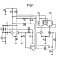
- FIGS. 1 and 2 With reference to Fig. 3 u. 4 The invention will now be described in more detail with reference to FIGS. 1 and 2.
- FIG. 1 in which the general principle of the transistor oscillator circuit according to the invention is shown, while FIG. 2 shows a particularly favorable embodiment in its details. Both versions can be implemented using bipolar transistors. In this context, however, it should be noted that both the oscillator and the mixing stage and the circuit parts to be used for the negative feedback on the oscillator can also be implemented using MOS technology.
- the two bipolar transistors T1 and T2 forming the oscillator in the circuit according to FIG. 1 are identical to one another and of the npn type. They are connected to their emitters and are connected via a resistor R1 to the second operating potential, which serves as a reference potential (ground) and is made available by a DC voltage source U1.
- the other pole of the DC voltage source U1 which supplies the first operating potential is connected to the collector of the transistor T1 or T2 of the oscillator via a resistor R7 or R8.
- the base of the transistor T1 forms the control input of the oscillator, since it is connected via a capacitor C1 to the frequency-determining control element of the oscillator.
- This tax body is either a pa parallel resonance circuit, i.e. a resonant circuit formed from a capacitor C with inductance L connected in parallel, which is on the one hand at the reference potential and on the other hand via the capacitor C1 at the control input T1 of the oscillator and via a further (same) capacitor C2 with the collector of the other transistor T2 Oscillator is connected.
- the resonant circuit can be serial. Then the inductance L is omitted at this point and the resonant circuit capacitor C is replaced by an inductor Ls exclusively connecting the two poles of the two coupling capacitors C1 and C2 facing away from the oscillator.
- the quartz crystal Q replaces the serial inductance Ls.
- the parallel inductance L and the parallel capacitor C are also omitted in this case.
- the base of transistor T1 is connected to the base of transistor T2 via two resistors R2 and R3 connected in series.
- the dividing point between these two resistors R2, R3 is connected to ground via the DC voltage source U3.
- Another capacitor C3 is provided between the base terminal of the second transistor T2 and the reference potential. Because of this feedback effect, which causes the oscillator effect of the differential amplifier T1, T2, between the base terminal of the transistor T1 and the collector terminal of the transistor T2, the collectors of the two transistors T1 and T2 are able to supply the subsequent mixer stage with the sine oscillations required to operate the circuit.
- the mixer stage consists of two pairs of transistors T3, T4 and T5, T6 which, like the transistors of the oscillator T1, T2, consist of transistors of the NPN type.
- the symmetrical mixing stage comes about because the Transistors T3 and T4 on the one hand and the transistors T5 and T6 on the other hand connected in pairs via their emitters and the collector of one transistor of the two pairs to the. an output terminal A1 and the collector of one of the two other transistors of the two pairs is connected to the other output terminal A2.
- the collector of transistor T3 and the collector of transistor T5 are at terminal A1
- the collector of transistor T4 and the collector of transistor T6 are at terminal A2 of the output of the mixer.
- the transistors T3 and T4 on the one hand and the transistors T5 and T6 on the other hand are combined into a pair via their emitters and each of the two pairs T3, T4 and T5, T6 via its emitters with the collector of a further npn transistor T7 or T8 connected.
- These transistors T7 and T8 are in turn combined by their emitters and connected via their emitters via a common resistor R4 to the common reference potential of the circuit.
- the transistors T3 and T6 form a first common input terminal via their base connections and the transistors T4 and T5 form a second common input terminal for the oscillator signal supplied by the oscillator output. Therefore, the base connections of transistors T3 and T6 are on the collector of transistor T1 and the base connections of transistors T4 and T5 of the mixer are on the collector of the other transistor T2 of the oscillator.
- the npn transistors T7 and T8 provided to act on the emitters of the first transistor pair T3, T4 on the one hand and of the second transistor pair T5, T6 of the mixer stage in turn serve as a signal input to the mixer stage and thus to the circuit. You are therefore in operation by an external signal, the z. B. is supplied by a (not shown) input amplifier, control For this purpose, the base of transistor T7 is connected to one input terminal E1 and the base of the other transistor'T8 to the other input terminal E2. Finally, the two transistors T7 and T8 provide the emitter potential required for the transistor pairs T3, T4 and T5, T6 of the mixer.
- a further DC voltage source U2 is provided, one pole of which is at the common reference potential, while the other pole is connected on the one hand to the base of the transistor T7 via a resistor R5 and to the base of the transistor T8 via a resistor R6.
- each of the two outputs of the oscillator that is, the collectors of the two transistors T1 and T2
- Resistor R9 and resistor R10 thus form a low-pass filter with capacitor C4, which is used to control one of the two inputs of the control amplifier.
- the signal output of the control amplifier V is located directly at the base of the transistor T2, which is not directly at the capacitor C1 and thus above it at the frequency-determining control element of the oscillator.
- the low-pass filter R9 and R10, C4 is dimensioned such that the appearance of the oscillator oscillation at the input of the control amplifier V is completely suppressed.
- the control amplifier V is expediently designed as an operational amplifier.
- the circuit of an oscillator-mixer combination in bipolar technology shown in FIG. 2 contains in principle the same circuit parts as are given in the circuit diagram according to FIG. 1. However, the circuit is much more detailed. It mainly consists of npn transistors and a few pnp transistors, as well as diodes, capacitors and resistors, so that, apart from the resonant circuit, the rest of the circuit can be easily summarized as monolithic. In addition to the circuit parts shown in FIG. 1, constant current sources serving, inter alia, to improve the desired effect and the operation of the oscillator and the mixing stage are provided.
- the resonant circuit designed in the example shown in FIG. 2 as a parallel resonant circuit and serving to fix the oscillator frequency is located above the two coupling capacitors 28 and 29 at the control input of the oscillator.
- the oscillator is in turn provided by two NPN transistors 33, 41, which correspond to transistors T1 and T2 according to FIG. 1 and are connected to their emitters.
- the resonant circuit 25 with its other connection at the reference potential (ground) lies with its first connection via the capacitor 28 on the collector of transistor 33 and via capacitor 29 at the base of transistor 41.
- the latter is also connected to the base of transistor 33 of the oscillator via a voltage divider consisting of the two resistors 68, 69.
- the dividing point of this voltage divider 68, 69 lies at the cathode of a diode 31, the anode of which is connected to the reference potential, that is to say ground.
- the cathode of the diode 31 is connected to the base of the transistor 33 and, on the other hand, via a resistor 30 to the output of a circuit part to be described and serving as a current source, while the anode of the diode 31 is at the reference potential.
- the collector of the oscillator transistor 33 and the collector of the oscillator transistor 41 are each via a resistor 34 or 38 am.Emitter each of a transistor 35 or 39 of the npn type, the collectors of which via a resistor 36 or 37 to that of a DC voltage source U1 delivered first operating potential are laid.
- the first operating potential is supplied by the positive terminal and the reference potential by the negative terminal of the DC voltage source U1.
- To generate the potential of the base connections of the two transistors 35 and 39 which serve to decouple the oscillator signal, these are connected via a resistor 40 to the positive pole of a further DC voltage source U4, which is also related to ground with its negative pole.
- the two cascode transistors 35 and 39 with their collectors form the two output connections of the oscillator.
- the emitters of the two oscillator transistors 33 and 41 are connected to the collector of an npn transistor 43, the emitter of which is combined with the emitter of two further transistors 44 and 45 (also of the npn type) also serving as current sources and over the collector-emitter path of a further npn transistor 54 and the resistor 55 is connected to the reference potential.
- the collector of the power supply transistor 44 is connected to the collector of the oscillator transistor 33 and the collector of the transistor 45 is connected to the collector of the oscillator transistor 41.
- the circuit means used to generate the base potentials of transistors 43, 44 and 45 will be discussed further below.
- the output connections of the oscillator that is to say the collectors of the npn transistors 35 and 39, are provided both for the feedback to be carried out according to the invention and for the loading of the mixing stage.
- the collector of transistor 35 is connected to the base of an npn transistor 120 and the collector of transistor 39 is connected to the base of an npn transistor 121.
- the collectors of these two transistors 120 and 121 are at the first operating potential, that is to say at the positive pole of the voltage source U1, and their emitter electrodes are each connected via a (similarly dimensioned) resistor 64 and 63, which in turn are connected to one another and connected to the reference potential of the circuit via a further resistor 24 are.
- the emitters of the two NPN transistors 120,. Serving as emitter followers for the mixing stage. 121 are connected to the inputs of the symmetrical mixer stage which are provided for the application by the oscillator.
- the mixer stage consists of the NPN transistors 107, 108, 109, 110, 111, 112 and 106 and 105, and the resistors 104, 122 and 123.
- the transistors 107 and 108 form the first transistor pair and the transistors 109 and 110 the second Transistor pair corresponding to the circuit shown in Fig. 1 for the balanced mixer.
- the combination of transistors 107 and 108 or 109 and 110 is in turn due to the connection of Emitters of the transistors of the relevant pair of transistors and their exposure to the collector of one npn transistor 106 or 105 assigned to the respective pair. As in FIG.
- transistors T7 and T8 are those which are to be processed externally via signal input 113
- Signal via their base connections to be controlled transistors 105 and 106 is also provided with the required base voltage by a further DC voltage source U2 via a resistor 122 and 123, respectively, while the emitters of these two transistors 105 and 106 are connected to the reference potential via a common resistor 104.
- the transistor 107 of the first and the transistor 110 of the second transistor pair of the mixer stage is controlled by the oscillator signal via the emitter of the transistor 120 operated as an emitter follower.
- transistor 108 of the first and transistor 109 of the second pair of the mixer stage are controlled by the emitter of transistor 121.
- the emitter of transistor 121 is also connected via a resistor 27 to the base of the circuit comprising transistors 11, which will be described below and 12.
- the collectors of transistor 107 and transistor 109 of the mixer stage jointly control the emitter of output transistor 111 (of the NPN type) and on the other hand the collectors of the two transistors 108 and 110 of the mixer stage jointly control the emitter of the second output transistor 112 (also of NPN type) ) the mixing level.
- the collectors of the two output transistors form the signal output 114 of the circuit.
- the base connections of the two output transistors 111 and 112 are connected together via the resistor 42 to the reference potential of the circuit.
- the collector of the oscillator transistor 33 is connected to the base of an npn transistor 70 and the collector of the oscillator transistor 41 is connected to the base of an npn transistor 73.
- the two last-mentioned transistors 70 and 73 are operated as emitter followers and are therefore with their collectors at the first operating potential supplied by the voltage source U1, while their emitters each have a resistor 71 and 72 (equally dimensioned) and a third - common - resistor 65 are at the reference potential of the circuit.
- the emitters of these two NPN transistors 70 and 73 are used to control two transistor combinations.
- the emitter of transistor 70 is connected on the one hand to the base of an npn transistor 67 and via a resistor 85 to the base of a further npn transistor 83, while the emitter of transistor 73 is connected to the base of an npn transistor 74 and above a resistor 84 is located at the base of the transistor 83 already mentioned.
- the npn transistor 83 is combined with a further npn transistor 82 to form a Darlington stage in that its emitter is directly connected to the base of the transistor 82 and its collector is connected to the collector of the transistor 82.
- the collectors of transistors 82, 83, 74 and 67 are at the first operating potential, that is, at the positive pole of U1.
- the emitters of the NPN transistors 67 and 74 are also connected to one another and are connected to the cathode of the diode 62 (which forms a capacitor), the anode of which is at the reference potential.
- the emitter of transistor 82 is connected to the base of a pnp transistor 86, the collector of which is connected to the reference potential and the emitter of which is connected to the cathode of a diode 87, the anode of which is connected to the base of a two-phase Collector pnp transistor 88 is connected.
- the one collector this transistor 88 is connected directly to the base of this transistor 88, the second collector of which is connected to the reference potential via the collector-emitter path of an npn transistor 96 and a resistor 98 connected to the emitter of this transistor 96.
- the emitter of the two-collector transistor 88 mentioned is connected on the one hand to the collector of a further pnp transistor 115 via a resistor 90 and to the emitter of a second pnp two-collector transistor 92 via a further resistor 91 which is the same as the resistor 90 .
- the connection of the two collectors and the base of the transistor 92 corresponds to the conditions in the two-collector transistor 88. Accordingly, the one collector and the base are connected directly to one another and are located on the anode of a diode 94, the cathode of which is connected to the emitter of a further pnp transistor 93.
- the collector of the last-mentioned pnp transistor 93 is at the reference potential.
- the second collector of the pnp transistor 92 is connected to the reference potential via the collector-emitter path of an npn transistor corresponding to the transistor 96 and a resistor 97 equal to the resistor 98. Both NPN transistors 95 and 96 form a base-coupled current source.
- the pnp transostor 115 mentioned in the last paragraph and intended to control the emitters of the two two-collector transostors 88 and 92 is connected with its emitter via a resistor 119 on the one hand to the first operating potential supplied by U1.
- the emitter of pnp transistor 116 is connected via resistor 118 to the first operating potential supplied by DC voltage source U1.
- the base of this further pnp transistor 116 is located across the resistor 117 both at the base of the pnp transistor 115 and on its own collector.
- the collector of the last presented PNP transistor 116 and therefore the base of the PNP transistor 115 are connected via the collector-emitter path of an npn - 100 connected transistor 99 and one connected to the emitter of this transistor 99 resistor to the reference potential of the circuit.
- the just introduced npn transistor 99 forms, together with another npn transistor 22, a constant current source.
- the collector of the npn transistor 22 is connected via a resistor 103 to the first operating potential supplied by U1 and with its emitter via the resistor 102 to the reference potential, while the base of the transistor 22 is connected via a resistor 101 to both its own collector and the Base of the npn transistor 99 is connected.
- the resistor 103 also serves to control the power supply of the oscillator transistors 33 and 41 in a manner to be described.
- the said collector of the two-collector pnp transistor 88 is located at the base of a pnp transistor 57 and via the resistor 59 at the positive pole of a further DC voltage source U3, which is already in connection with the control of the oscillator via the base connections of the transistors 33 and 41 connecting voltage divider 68, 69 was called.
- the pnp transistor 58 which is controlled by the collectors of the two-collector transistor 88 and the transistor 96, has its collector at the reference potential and its emitter at the base of a first npn transistor 57 and at the emitter of a further npn transistor 50.
- the collector of these two transistors 56 and 57 is at the first operating potential supplied by the DC voltage source U1.
- the transistor combination 56, 58 is used to clamp the maximum possible voltage at the base 57.
- the emitter of the npn transistor 57 is connected to the base of the npn transistors 44 and 45 already mentioned in connection with the oscillator transistors 33 and 41.
- the emitters of the npn transistors 70 and 73 provided at the input of the negative feedback branch of the oscillator and already mentioned are provided for controlling three npn transistors 67, 74 and 83.
- the emitters of the two transistors 67 and 74 are connected together and are connected to the cathode of a diode 62, the anode of which is held at the reference potential.
- Another diode 61 is also connected to the reference potential with the anode and to the base of the npn transistor 83 with the cathode and thus at the input of the Darlington stage composed of the transistors 82 and 83.
- the emitters of the two npn transistors 67 and 74 connected to the base of an npn transistor 66, the collector of which at the first operating potential (supplied by U1) and the emitter of the collector and emitter of a further npn transistor 75, and via a resistor 79 both at the base of the one already in connection with the second two Collector transistor 92 mentioned pnp transistor 93 and also via a further resistor 80 on the collector of a further npn transistor 77.
- the collector of the last-mentioned npn transistor 77 is also connected via a resistor 76 to the emitter of the npn transistor 75 connected as a diode.
- the emitter of the last introduced npn transistor 77 is connected to the reference potential via a resistor 78.
- the base of this transistor is already with the base of the in connection with the Darlington stage from the npn transistors 82, 83 introduced and their emitters for.
- Reference potential leading npn transistor 81 connected. Both basic connections are supplied via a fifth DC voltage source U5, the negative pole of which is at the operating potential.
- Another constant current source consists of the base-coupled npn transistors 3 and 4, the emitter of transistor 3 being connected directly and the emitter of transistor 5 being connected to the reference potential of the circuit via said resistor 5.
- the collector of the transistor 3 is connected to its own base and via a resistor 1 to the first operating potential.
- the collector of the second transistor 4 of the current source (ie its output) is connected to the collector of a further pnp transistor 6, the emitter of which is connected to the base of a further npn transistor 9 via a resistor 2 at the first operating potential and the base of which is connected via a resistor 7 is.
- a resistor 8 forms the connection of the emitter of this further npn transistor 9 to the first operating potential.
- the collector of the pnp transistor 9 is connected to the collector of two further npn transistors 11 and 12.
- the base of the first of these npn transistors leads via the resistor 26 to the base connection of the transistor 107 and to the base connection of the transistor 110 of the mixer stage and thus to the signal input to be applied to it by the oscillator.
- the base of the second of these npn transistors namely transistor 12, leads via resistor 27 to the base connections of transistors 108 and 109, and thus also to that input of the balanced mixer which is controlled by the other output of the oscillator.
- the base connections of the last introduced npn transistors 11 and 12 are bridged before the resistors 26 and 27 by two diodes which produce the desired low-pass effect.
- the base of the transistor 11 is connected to the anode of the diode 21 and the cathode of this diode 21 to the base of the npn transistor 12.
- the anode is directly connected to the base of the npn transistor 12 and the cathode to the pole of the base of the transistor 11.
- the collector terminals of the NPN transistors 11 and 12 are, as already mentioned, common to the q by the transistor 9, the transistors 3, 4, 6 and 9 containing constant current supplied ource.
- the signal output of the two npn transistors 11 and 12 is given by their emitter connections, which for this purpose are connected to the emitter of a pnp transistor 13 and 14, respectively.
- the base of the pnp transistor 13 and the pnp transistor 14 is connected directly to the collector of the power supply transistor 4 already mentioned.
- the collectors of the two last-mentioned pnp transistors 13 and 14 are located across the collector-emitter path of an npn transistor 17 or 18 and a resistor 19 or 16 connected upstream of the emitter of the relevant transistor 17 or 18 at the reference potential of the circuit.
- the two transistors 17 and 18 are directly connected to their base connections, the base of the transistor 18 also being short-circuited to its own collector, and so this transistor 18 is connected as a diode.
- the base of the two npn transistors 17 and 18 is connected to the anode of a diode 15, the cathode of which is connected to the collector of the npn transistor 17 and thus to the collector of the pnp transistor 13.
- the collectors of the transistors 17 and 13 via the already mentioned resistor 30 to the base of the oscillator sistor 33 and thus fed back to the oscillator.
- npn transistors 45 and 46 which have already been mentioned repeatedly in connection with the two oscillator transistors 33 and 41, receive their operating potential from the collector of an npn transistor 54, the emitter of which via a resistor 55, just like the emitter of the npn transistor 43, which has also already been presented is acted upon by the reference potential.
- Another npn transistor 52 is also connected to the reference potential with its emitter via the resistor 53, while its collector is connected on the one hand to the base of the above-mentioned npn transistor 44 or 45 and to the emitter of a further npn transistor 57 .
- the base connections of the three npn transistors 48, 52 and 54 are all connected to the collector of the power supply transistor 22 and thus also to the resistor 103, which establishes the connection to the first operating potential (DC voltage source U1) of the circuit.
- the npn transistor 46 also has its collector at the first operating potential, while the base potential of this transistor 46 is identical to the base potential of the pnp transistor 58 already mentioned in connection with the npn transistors 56 and 57 and the base potential of the now transistor 56 and is at the positive pole of the DC voltage source U3.
- the control amplifier in the feedback of the oscillator is through the input transistor 86, the diode 87, the two two-collector transistors 88 and 92, the diode 94 and the transistor 93, and the npn transistors 95 and 96 given.
- the input of the feedback is given by the two transistors 70 and 73.
- the opposite phase signal to the signal at the emitters of the two transistors 70 and 73 is generated by summation from the emitter of the two transistors 70 and 73 via the two resistors 84 and 85 to the base of the transistor 83. Residual components are grounded via the diode 61, so that the two resistors 84 and 85 in combination with the diode 61 act as a low pass.
- the reference value at the base of transistor 83 is obtained. This reference value is passed on via the emitter of transistor 83, the base of transistor 82 and the emitter of transistor 82 to the input transistor of the control amplifier, that is to say the base of pnp transistor 86.
- the antiphase signal at the emitters of transistors 70 and 73 is also routed to the base of transistors 67 and 74.
- the emitter of these transistors 67 and 74 is capacitively blocked against ground, that is to say the reference potential, via the diode 62 and is supplied with respect to the required emitter voltage from the base of the transistor 66. Thanks to the peak rectification of the transistors 67 and 74, an additional DC voltage potential is now formed on the diode 62 in accordance with the oscillator amplitude. This potential is passed on to the short-circuited base-collector path of transistor 75 via the emitter of transistor 66. The emitter of transistor 75 is supplied via resistor 76 from the collector of transistor 77 with the required operating current.
- the emitter of transistor 66 is connected to resistor 79.
- Resistor 80 goes from resistor 79 to the collector of transistor 77 and resistor 76 to the emitter of the transistor 75.
- the ratio of the resistance values in the dividers 79 and 80 sets a DC voltage value which is proportional to the voltage change at the emitters of the transistors 67 and 74. This gives the control amplifier its lead.
- the lead of the control amplifier is set via the voltage dividers 79 and 80 and thus also the oscillator amplitude.
- the output transistors 35 and 39 provided in the oscillator serve to ensure that the disturbances which originate from the input 113 of the mixer stage and which are present at the collector of these output transistors, as a result of the low collector-emitter reaction of the transistors 35, 39, are only greatly weakened on the Oscillator circuit can make noticeable.
- the signal at the base of the transistors 11 and 12 is amplified via the cascode stage 13 and 14 and the current mirror 17, 18.
- the diodes 31 and 15 serve to suppress control oscillations.
- the diodes 20 and 21 short-circuit the antiphase signal at the output of the resistors 26 and 27. This will. only the direct current component and at most components of very low frequency left to the control amplifier 11, 12.
- the control amplifier 86, 87 serves to control the oscillator amplitude via the push-pull current output, which is given by the collectors of the transistors 88 and 96, via the base of the transistor 57.
- the load resistor which sets the voltage is given by resistor 59.
- the control amplifier 11, 12 etc. on the other hand, has the task of reducing the asymmetry at the mixer.
- the further invention relates mainly to a further improvement of the transistor oscillator circuit described so far.
- the further invention also has advantages if it is applied to an oscillator circuit or quartz-controlled oscillator, which is provided by a feedback differential amplifier, even if the said oscillator is not intended to act on a mixer stage.
- the invention provides that the capacitor in the frequency-determining control element has its one connection to the first coupling capacitor leading to the first transistor of the differential amplifier and with. its second connection is directly connected to the second coupling capacitor leading to the collector of the second transistor of the differential amplifier, so that a further capacitor is provided in the frequency-determining control element in such a way that this further capacitor has one connection with that of the second Transistor of the differential amplifier facing away connection of the second coupling capacitor is connected directly and via a resistor to one pole of a third DC voltage source, while the other connection of this further capacitor in the frequency-determining controller n and the other pole of the third DC voltage source directly at the supply terminal of the reference potential Oscillator circuit lie.
- FIG. 3 A transistor oscillator circuit improved in this sense is shown in FIG. 3, while the oscillator circuit shown in FIG. 4 additionally corresponds to the previously described transistor oscillator circuit.
- the two bipolar transistors T1 and T2 forming the oscillator in the circuit according to FIGS. 3 and 4 are identical to one another and of the nph type. They are directly connected to their emitters and these emitters are connected via a common resistor R1 to the supply terminal of the circuit, ie to ground, which carries the reference potential.
- the supply terminal of the oscillator circuit which provides the first operating potential is connected to the positive pole, the terminal of the oscillator circuit which supplies the reference potential is connected directly to the negative pole of a first DC voltage source U1.
- the base of the first transistor T1 of the differential amplifier forms the one of the oscillator connected to the frequency-determining element, a first coupling capacitor C1 being provided between these two circuit parts.
- the above-mentioned frequency-determining control element is either a parallel resonance circuit (that is, it is formed from a capacitor with inductance connected in parallel ter resonant circuit), which is connected on the one hand to the supply terminal carrying the reference potential and on the other hand to the first coupling capacitor C1 leading to the base of the first transistor T1 of the differential amplifier.
- said control element can be provided by a serial resonant circuit. Then, the inductance L placed parallel to the resonant circuit capacitor in the circuits according to FIGS. 3 and 4 is replaced by an inductance which then forms the only connection between the connections of the two coupling capacitors C1 and C2 facing away from the transistors of the differential amplifiers T1 and T2. Finally, an inductance in the control element can be completely dispensed with and instead the two connections of a quartz oscillator capacitor can be connected to one of the two connections of the first and second coupling capacitors C1 and C2 not connected to one of the transistors T1 or T2. A particularly advantageous connection of the oscillating quartz capacitor is described further below as a further embodiment of an oscillator according to the invention.
- the base of the first transistor T1 of the differential amplifier is connected to the base of the second transistor T2 of the differential amplifier via two resistors R3 and R2 connected in series. s tärkers connected.
- the dividing point between these two resistors R2 and R3 is connected to the positive pole of the second DC voltage source according to the definition of the invention, that is to say the DC voltage source U3, while the other pole of this DC voltage source is connected to the supply terminal which carries the reference potential, that is to say the negative pole of the DC voltage source U1 , is created.
- Another capacitor C3 is provided between the base terminal of the second transistor T2 of the differential amplifier and the supply terminal carrying the reference potential.
- the collectors of these two oscillator transistors T1 and T2 are able to emit an undamped sine wave together. They accordingly form the two output terminals A1 * and A2 * of the oscillator according to FIG. 1.
- these two output terminals A1 and A2 are connected to two input transistors T3 and T6 of the mixer stage to be loaded.
- the series circuit of two capacitors C 'and C is provided in the control circuit of a transistor oscillator corresponding to the further invention instead of a single resonant circuit capacitor C as in the case of the disclosures of the main application.
- These two transistors C 'and C together form a capacitive voltage divider.
- the resonant circuit inductance L forms a connection between the two end connections of the voltage divider C ', C *, which bridges the two capacitors and bridges the divider point and also with one Connection at the supply terminal carrying the reference potential. In the case of a series resonant circuit this inductance L drops. Instead, an inductance bridging the two coupling capacitors C1 and C2 is provided. If the oscillator is to be controlled by a quartz oscillator instead, the capacitor containing the quartz oscillator takes the place of the inductance to be used if a series resonant circuit is used.
- the voltage divider formed from the two capacitors C 'and C is provided, the connection of this voltage divider to the two coupling capacitors C1 and C2, to the reference potential, to the resistor R and the DC voltage source U always that of FIGS. 1 and Fig. 2 apparent configuration corresponds.
- the second coupling capacitor C2 is provided by a quartz crystal.
- the free capacitor of the voltage divider C ' is connected with its free connection to the first coupling capacitor C1 and, via this, to the base of the first oscillator transistor T1.
- the free capacitor of the second capacitor C * of the capacitive voltage divider is connected to the supply terminal carrying the reference potential, to which the negative pole of the third DC voltage source U * is also connected.
- the positive pole of the third DC voltage source U * is via the resistor R according to the definition of the invention on the one hand with the dividing point, i.e. a circuit point between the two capacitors C 'and C * of the capacitive voltage divider and on the other hand with the connection of the second coupling capacitor C2 facing away from T2 connected.
- the circuit inductance L is at the end connections of the capacitive voltage divider C ', C *.
- the previously customary and constructed using a differential amplifier T1, T2 are so-called two-point oscillators, in which the base of the one transistor T1 is galvanically or capacitively connected to the collector of the second transistor T2 of the differential amplifier.
- the center point of this connection lies at the high point of a parallel resonant circuit or at the intermediate point of a series resonant resonant circuit.
- the negative steepness of the admittance curve of these coupling points ensures that the oscillation at the output of the oscillator is retained.
- the blind components of this slope lead both to an annoying frequency drift and to a reduction in the tuning range.
- the finite gain from the base of the second transistor T2 of the differential amplifier to the output of the amplifier at the collector of the transistor T2 is not always sufficient to maintain the oscillation state.
- an oscillating circuit or oscillating-gauze control circuit controlling the input of such an oscillator is equipped with a series capacitance C ', C * instead of a simple capacitor C and the high point or midpoint of such an oscillating circuit or quartz control circuit corresponding to that of Coupled with the invention given proposals to the oscillator transistors T1 and T2, the parasitic capacitive and real portion of the active circuit in the overall resonant circuit or quartz control circuit is significantly reduced. This increases the frequency variation range, increases vibration security and drastically reduces the tendency to frequency drift.
- the capacitor C 'of the capacitive voltage divider C', C in the form of a, which is located on the first coupling capacitor C1 Realize capacitance diode.
- the other capacitor C can also be provided by a capacitance diode, which is recommended, for example, for the cable television sector or for the FM region.
- the capacitance of the two capacitors C 'and C can be influenced by means of the potential supplied by the third direct voltage source U and applied to the resistor R, in particular if at least one of these two capacitors is provided by a semiconductor capacitance diode, ie a varactor diode or a normal pn junction diode.
- the influencing of the capacitances C 'and C has an advantageous effect on the setting range for the oscillation frequency.
- the first coupling capacitor C1 can also be connected in series with a further capacitance diode, which is then expediently used between the coupling capacitor C1 and the first capacitor C 'of the capacitive voltage divider C', C.
- the coupling capacitor C2 leading to the collector of the second transistor of the differential amplifier can be replaced by an oscillating quartz crystal, so that the circuit for an oscillator controlled oscillator according to the invention can be somewhat simplified in this way.
- This also eliminates the direct connection between the two coupling capacitors C1 and C2, which is present in the other case of the circuit described above when using a quartz crystal control. This leads to a so-called overtone oscillator.
- the symmetrical mixer stage arises because the npn transistors T3 and T4 on the one hand and the npn transistors T5 and T6 on the other hand are connected in pairs via their emitters and the collector of a transistor of the two pairs to the one output terminal A1 and the One of the two other transistors of the two pairs is connected to the other output terminal A2.
- the col detector of transistor T3 and the collector of transistor T5 at terminal A1 the collector of transistor -T4 and the collector of transistor T6 at terminal A2 of the output of the mixer.
- the transistors T3 and T6 as well as the transistors T5 and T4 are combined to form a pair of transistors via their base connections, in that the two transistors T3 and T6 together from the collector of the first oscillator transistor T1 and the two transistors T4 and T5 together from the collector of the second oscillator transistor T2 can be controlled via their basic connections.
- the emitters of transistors T3 and T4 are connected to the collector of a further npn transistor T7 and the emitters of transistors T5 and T6 are connected to the collector of a sixth npn transistor of the mixing stage, which is designated T8.
- the emitters of the two last-mentioned npn transistors T7 and T8 are connected to the reference potential via a common emitter series resistor, that is to say to the supply terminal for the reference potential defined above.
- the emitter series resistor of T7 and T8 is resistor R4.
- a fourth DC voltage source U2 lies with its nega-pole at said power supply terminal for the B ezugspo- tential and with its positive pole via a resistor R5 or R6 to the base of transistor T7 unddes transistor T8.
- the base connections of the two transistors T7 and T8 each form a connection E1, E2 to be processed jointly by an external signal to be processed, for example via a preamplifier (not shown), that is to say maW, the signal input of the mixing stage.
- each of the two output terminals A1, A2 * of the oscillator that is, the collector of the oscillator transistor T1 and T2, via a resistor R9 or R10 to each input of a control amplifier V.
- the two resistors R9 and R10 are connected to one another at the connection facing away from the transistor T1 and T2 via a capacitor C4.
- the resistor R9 and the resistor R10 thus form a low-pass filter with the capacitor C4, through which the control amplifier V is controlled.
- the signal output of the control amplifier V is located directly at the base of the second oscillator transistor T2.
- the low-pass filter R9, R10, C4 is dimensioned so that the occurrence of the oscillator oscillation at the input of the control amplifier V is completely suppressed. This leads to the negative feedback leading via the control amplifier V becoming purely direct current. The consequence of this is that the inevitably inevitable asymmetry of the potential changes at the two output terminals A1, A2 * of the oscillator is reduced. This has the effect of suppressing the oscillator noise and compensating for further interference originating from the oscillator on the IF signal supplied by the output A1, A2 of the mixer stage.
- the capacitor C provided there in the resonant circuit 25 as a voltage divider from two series-connected capacitors C ', C * and this - together with another DC voltage source corresponding to the DC voltage 1 and 2 of the present application to the capacitor 28 which corresponds to the first coupling capacitor C1 and to the capacitor 29 which corresponds to the second coupling capacitor C2.
Landscapes
- Engineering & Computer Science (AREA)
- Power Engineering (AREA)
- Inductance-Capacitance Distribution Constants And Capacitance-Resistance Oscillators (AREA)
- Oscillators With Electromechanical Resonators (AREA)
Applications Claiming Priority (4)
| Application Number | Priority Date | Filing Date | Title |
|---|---|---|---|
| DE3041392 | 1980-11-03 | ||
| DE3041392A DE3041392C2 (de) | 1980-11-03 | 1980-11-03 | Oszillatorschaltung mit einer Mischstufe |
| DE3045993 | 1980-12-05 | ||
| DE19803045993 DE3045993A1 (de) | 1980-12-05 | 1980-12-05 | Transistor-oszillatorschaltung |
Publications (2)
| Publication Number | Publication Date |
|---|---|
| EP0051179A1 true EP0051179A1 (fr) | 1982-05-12 |
| EP0051179B1 EP0051179B1 (fr) | 1984-09-19 |
Family
ID=25788888
Family Applications (1)
| Application Number | Title | Priority Date | Filing Date |
|---|---|---|---|
| EP81108332A Expired EP0051179B1 (fr) | 1980-11-03 | 1981-10-14 | Circuit oscillateur pouvant être intégré |
Country Status (3)
| Country | Link |
|---|---|
| US (1) | US4479259A (fr) |
| EP (1) | EP0051179B1 (fr) |
| DE (1) | DE3166196D1 (fr) |
Cited By (10)
| Publication number | Priority date | Publication date | Assignee | Title |
|---|---|---|---|---|
| EP0167007A1 (fr) * | 1984-06-07 | 1986-01-08 | Siemens Aktiengesellschaft | Circuit oscillateur-mélangeur |
| EP0223228A2 (fr) * | 1985-11-21 | 1987-05-27 | Motorola, Inc. | Oscillateur équilibré |
| EP0226255A2 (fr) * | 1985-12-19 | 1987-06-24 | Philips Patentverwaltung GmbH | Modulateur |
| EP0299215A1 (fr) * | 1987-07-17 | 1989-01-18 | Siemens Aktiengesellschaft | Circuit de régulation monolithique |
| EP0299464A1 (fr) * | 1987-07-17 | 1989-01-18 | Siemens Aktiengesellschaft | Oscillateur-amplificateur monolithique réglable en amplitude |
| EP0301319A1 (fr) * | 1987-07-17 | 1989-02-01 | Siemens Aktiengesellschaft | Circuit oscillateur-amplificateur différentiel monolithique réglé en amplitude |
| FR2635424A1 (fr) * | 1988-07-29 | 1990-02-16 | Toshiba Kk | Modulateur et emetteur |
| EP0455711A1 (fr) * | 1989-01-27 | 1991-11-13 | Motorola Inc | Etage heterodyne a commande precise en boucle fermee de l'amplitude du signal d'injection. |
| EP0474729A1 (fr) * | 1989-06-02 | 1992-03-18 | Motorola Inc | Oscillateur a tension controlee muni d'un regulateur de courant automatique. |
| EP0726646A1 (fr) * | 1995-02-13 | 1996-08-14 | Kabushiki Kaisha Toshiba | Converteur de fréquences capable de réduire les composantes de bruit dans des signaux d'oscillations locales |
Families Citing this family (25)
| Publication number | Priority date | Publication date | Assignee | Title |
|---|---|---|---|---|
| NL8301099A (nl) * | 1983-03-29 | 1984-10-16 | Philips Nv | Afstembare ontvangeringangsschakeling. |
| JPS6115426A (ja) * | 1984-06-29 | 1986-01-23 | Matsushita Electric Ind Co Ltd | ミキサ装置 |
| US4677691A (en) * | 1985-08-01 | 1987-06-30 | Texas Instruments Incorporated | Microwave receiver |
| US5053726A (en) * | 1990-04-10 | 1991-10-01 | Thomson Consumer Electronics, Inc. | Circuit for preventing VCXO mode jumping |
| JPH05268109A (ja) * | 1992-03-23 | 1993-10-15 | Sony Corp | 受信機用ic及びこれを使用した受信機 |
| JPH05275924A (ja) * | 1992-03-26 | 1993-10-22 | Alps Electric Co Ltd | 高周波発振回路 |
| US6138000A (en) * | 1995-08-21 | 2000-10-24 | Philips Electronics North America Corporation | Low voltage temperature and Vcc compensated RF mixer |
| EP0954093A1 (fr) * | 1998-04-29 | 1999-11-03 | Mitel, Inc. | Suppression des harmoniques d' ordre pair d' un oscillateur local |
| US6194973B1 (en) * | 1998-05-29 | 2001-02-27 | Intel Corporation | Oscillator with automatic gain control |
| US6094105A (en) * | 1998-05-29 | 2000-07-25 | Intel Corporation | Oscillator with digital frequency control |
| SG81929A1 (en) * | 1998-06-01 | 2001-07-24 | Inst Of Microelectronics | Accurate and tuneable active differential phase splitters in rfic wireless applications |
| SE519333C2 (sv) * | 2000-08-25 | 2003-02-18 | Ericsson Telefon Ab L M | Blandare innefattande brusreducerande passivt filter |
| GB0030694D0 (en) * | 2000-12-15 | 2001-01-31 | Nokia Mobile Phones Ltd | An electronic circuit supplied with power via current generator means |
| US6889038B2 (en) * | 2001-04-06 | 2005-05-03 | Koninklijke Philips Electronics N.V. | Dynamic biasing of a transmitter |
| JP4365575B2 (ja) * | 2002-11-20 | 2009-11-18 | アルプス電気株式会社 | テレビジョンチューナの発振回路 |
| JP4015008B2 (ja) * | 2002-11-21 | 2007-11-28 | 株式会社ルネサステクノロジ | 通信用半導体集積回路および無線通信システム |
| EP1505720B1 (fr) * | 2003-08-06 | 2018-07-18 | Synergy Microwave Corporation | Oscillateur accordable en fréquence à faible bruit de phase et faible dérive thermique |
| JP4271634B2 (ja) * | 2003-09-17 | 2009-06-03 | 日本電波工業株式会社 | 水晶発振回路 |
| US7049878B2 (en) * | 2004-06-03 | 2006-05-23 | Winbond Electronics Corp. | Down-converter using an on-chip bias circuit for enhancing symmetry and linearity and testing device thereof |
| WO2006127442A1 (fr) * | 2005-05-20 | 2006-11-30 | Synergy Microwave Corporation | Oscillateur accordable possedant des circuits resonants accordes serie et parallele |
| EP1764914B1 (fr) * | 2005-09-14 | 2009-02-25 | CSEM Centre Suisse d'Electronique et de Microtechnique SA Recherche et Développement | Amplificateur différentiel sélectif à faible bruit |
| CA2566283C (fr) * | 2005-11-02 | 2011-10-18 | Synergy Microwave Corporation | Oscillateur accordable a definition de l'utilisateur, cout peu eleve, faible saut de phase et spectre pur |
| JP5568207B2 (ja) * | 2005-11-15 | 2014-08-06 | シナジー マイクロウェーブ コーポレーション | ユーザ指定可能、低コスト、低ノイズであり、位相跳躍に影響されにくいマルチオクターブ帯域チューナブル発振器 |
| EP1999921B1 (fr) * | 2006-03-29 | 2017-06-14 | Thomson Licensing DTV | Amplificateur limiteur de fréquences de module de translation de fréquences |
| US20090131000A1 (en) * | 2007-11-21 | 2009-05-21 | Kuo Yao H | Radio receiver system |
Citations (4)
| Publication number | Priority date | Publication date | Assignee | Title |
|---|---|---|---|---|
| DE2038435A1 (de) * | 1970-08-01 | 1972-02-10 | Standard Elek K Lorenz Ag | Oszillator |
| US4058771A (en) * | 1975-10-27 | 1977-11-15 | Sony Corporation | Double-balanced frequency converter |
| DE2850778A1 (de) * | 1977-11-28 | 1979-05-31 | Tokyo Shibaura Electric Co | Frequenzwandlerschaltung |
| US4227095A (en) * | 1978-06-30 | 1980-10-07 | King Radio Corporation | Deviation driver circuit |
Family Cites Families (2)
| Publication number | Priority date | Publication date | Assignee | Title |
|---|---|---|---|---|
| US3325747A (en) * | 1966-04-14 | 1967-06-13 | Hammond Organ Co | Plural frequency musical instrument oscillator |
| US3775702A (en) * | 1972-03-16 | 1973-11-27 | North Electric Co | Transistor inverter circuit for supplying constant current output |
-
1981
- 1981-10-14 EP EP81108332A patent/EP0051179B1/fr not_active Expired
- 1981-10-14 DE DE8181108332T patent/DE3166196D1/de not_active Expired
- 1981-10-21 US US06/313,629 patent/US4479259A/en not_active Expired - Fee Related
Patent Citations (4)
| Publication number | Priority date | Publication date | Assignee | Title |
|---|---|---|---|---|
| DE2038435A1 (de) * | 1970-08-01 | 1972-02-10 | Standard Elek K Lorenz Ag | Oszillator |
| US4058771A (en) * | 1975-10-27 | 1977-11-15 | Sony Corporation | Double-balanced frequency converter |
| DE2850778A1 (de) * | 1977-11-28 | 1979-05-31 | Tokyo Shibaura Electric Co | Frequenzwandlerschaltung |
| US4227095A (en) * | 1978-06-30 | 1980-10-07 | King Radio Corporation | Deviation driver circuit |
Non-Patent Citations (2)
| Title |
|---|
| FUNKSCHAU, Nr. 15, 1971 G. PELTZ "Zweipolige Oszillatorschaltungen für Parallel- und Serienresonanz" Seiten 465 bis 466 * |
| IEEE INTERNATIONAL SOLID STATE CIRCUITS CONF., Band XXII, Februar 1979 S. KOMATSU et al. "Session XVII: Linear Circuit Techniques" Seiten 236, 237 und 296 * |
Cited By (16)
| Publication number | Priority date | Publication date | Assignee | Title |
|---|---|---|---|---|
| EP0167007A1 (fr) * | 1984-06-07 | 1986-01-08 | Siemens Aktiengesellschaft | Circuit oscillateur-mélangeur |
| US4635003A (en) * | 1984-06-07 | 1987-01-06 | Siemens Aktiengesellschaft | Oscillator mixer circuit with reaction-tree coupling |
| EP0223228A2 (fr) * | 1985-11-21 | 1987-05-27 | Motorola, Inc. | Oscillateur équilibré |
| EP0223228A3 (en) * | 1985-11-21 | 1988-11-23 | Motorola, Inc. | Balanced oscillator |
| EP0226255A2 (fr) * | 1985-12-19 | 1987-06-24 | Philips Patentverwaltung GmbH | Modulateur |
| EP0226255A3 (en) * | 1985-12-19 | 1988-10-05 | Philips Patentverwaltung Gmbh | Modulator |
| EP0301319A1 (fr) * | 1987-07-17 | 1989-02-01 | Siemens Aktiengesellschaft | Circuit oscillateur-amplificateur différentiel monolithique réglé en amplitude |
| EP0299464A1 (fr) * | 1987-07-17 | 1989-01-18 | Siemens Aktiengesellschaft | Oscillateur-amplificateur monolithique réglable en amplitude |
| EP0299215A1 (fr) * | 1987-07-17 | 1989-01-18 | Siemens Aktiengesellschaft | Circuit de régulation monolithique |
| FR2635424A1 (fr) * | 1988-07-29 | 1990-02-16 | Toshiba Kk | Modulateur et emetteur |
| EP0455711A1 (fr) * | 1989-01-27 | 1991-11-13 | Motorola Inc | Etage heterodyne a commande precise en boucle fermee de l'amplitude du signal d'injection. |
| EP0455711A4 (en) * | 1989-01-27 | 1992-10-28 | Motorola, Inc. | Heterodyne stage having precise closed-loop control of the amplitude of the injection signal thereof |
| EP0474729A1 (fr) * | 1989-06-02 | 1992-03-18 | Motorola Inc | Oscillateur a tension controlee muni d'un regulateur de courant automatique. |
| EP0474729A4 (en) * | 1989-06-02 | 1993-02-24 | Motorola, Inc. | Voltage control oscillator with automatic current control |
| EP0726646A1 (fr) * | 1995-02-13 | 1996-08-14 | Kabushiki Kaisha Toshiba | Converteur de fréquences capable de réduire les composantes de bruit dans des signaux d'oscillations locales |
| US5634207A (en) * | 1995-02-13 | 1997-05-27 | Kabushiki Kaisha Toshiba | Frequency converter capable of reducing noise components in local oscillation signals |
Also Published As
| Publication number | Publication date |
|---|---|
| US4479259A (en) | 1984-10-23 |
| DE3166196D1 (en) | 1984-10-25 |
| EP0051179B1 (fr) | 1984-09-19 |
Similar Documents
| Publication | Publication Date | Title |
|---|---|---|
| EP0051179B1 (fr) | Circuit oscillateur pouvant être intégré | |
| DE2850778A1 (de) | Frequenzwandlerschaltung | |
| DE19652146B4 (de) | Rauscharme Oszillatorschaltung | |
| EP0073929B1 (fr) | Circuit semi-conducteur de traitement de signaux réalisable en circuit intégré | |
| DE10232861A1 (de) | Frequenzverdoppler-Schaltungsanordnung | |
| DE19611610A1 (de) | Oszillaotr | |
| DE3041392C2 (de) | Oszillatorschaltung mit einer Mischstufe | |
| EP0975087A1 (fr) | Circuit oscillateur | |
| EP0077500A2 (fr) | Diviseur de fréquence intégrable | |
| DE3032661C2 (fr) | ||
| DE3005764C2 (de) | Regelbarer Oszillator | |
| DE2624133C3 (de) | Mischeranordnung | |
| EP0141933B1 (fr) | Oscillateur à circuit intégré | |
| EP0462304B1 (fr) | Montage de réglage en amplitude d'un oscillateur | |
| DE69219254T2 (de) | Audioverstärker | |
| DE3103204C2 (de) | Integrierte Schaltung mit einem Substrat und mit mindestens zwei Verstärkerstufen | |
| DE3221267C2 (fr) | ||
| DE3125200C2 (de) | Rückführungsstabilisierter Zwischenfrequenzverstärker für Fernsehzwecke | |
| EP0085872B1 (fr) | Amplificateur différentiel intégrable | |
| DE3319364C2 (de) | Spannungsgesteuerter Oszillator | |
| DE2949779A1 (de) | Verstaerkersystem mit automatischer verstaerkungsregelung, beispielsweise fuer einen am-rundfunkempfaenger | |
| EP0133618A1 (fr) | Circuit oscillateur haute fréquence à quartz sous forme de circuit intégré monolithique | |
| DE3624391A1 (de) | Verstaerkungseinstellschaltung | |
| DE3045993A1 (de) | Transistor-oszillatorschaltung | |
| DE2364187A1 (de) | Gesteuerter oszillator |
Legal Events
| Date | Code | Title | Description |
|---|---|---|---|
| PUAI | Public reference made under article 153(3) epc to a published international application that has entered the european phase |
Free format text: ORIGINAL CODE: 0009012 |
|
| 17P | Request for examination filed |
Effective date: 19811014 |
|
| AK | Designated contracting states |
Designated state(s): DE FR GB IT |
|
| ITF | It: translation for a ep patent filed | ||
| GRAA | (expected) grant |
Free format text: ORIGINAL CODE: 0009210 |
|
| AK | Designated contracting states |
Designated state(s): DE FR GB IT |
|
| REF | Corresponds to: |
Ref document number: 3166196 Country of ref document: DE Date of ref document: 19841025 |
|
| ET | Fr: translation filed | ||
| PLBE | No opposition filed within time limit |
Free format text: ORIGINAL CODE: 0009261 |
|
| STAA | Information on the status of an ep patent application or granted ep patent |
Free format text: STATUS: NO OPPOSITION FILED WITHIN TIME LIMIT |
|
| 26N | No opposition filed | ||
| ITTA | It: last paid annual fee | ||
| PGFP | Annual fee paid to national office [announced via postgrant information from national office to epo] |
Ref country code: GB Payment date: 19920914 Year of fee payment: 12 |
|
| PGFP | Annual fee paid to national office [announced via postgrant information from national office to epo] |
Ref country code: FR Payment date: 19921016 Year of fee payment: 12 |
|
| PGFP | Annual fee paid to national office [announced via postgrant information from national office to epo] |
Ref country code: DE Payment date: 19921216 Year of fee payment: 12 |
|
| PG25 | Lapsed in a contracting state [announced via postgrant information from national office to epo] |
Ref country code: GB Effective date: 19931014 |
|
| GBPC | Gb: european patent ceased through non-payment of renewal fee |
Effective date: 19931014 |
|
| PG25 | Lapsed in a contracting state [announced via postgrant information from national office to epo] |
Ref country code: FR Effective date: 19940630 |
|
| PG25 | Lapsed in a contracting state [announced via postgrant information from national office to epo] |
Ref country code: DE Effective date: 19940701 |
|
| REG | Reference to a national code |
Ref country code: FR Ref legal event code: ST |