EP0048805B1 - Semiconductor integrated circuit optical image-to-electrical signal transducer - Google Patents
Semiconductor integrated circuit optical image-to-electrical signal transducer Download PDFInfo
- Publication number
- EP0048805B1 EP0048805B1 EP81106125A EP81106125A EP0048805B1 EP 0048805 B1 EP0048805 B1 EP 0048805B1 EP 81106125 A EP81106125 A EP 81106125A EP 81106125 A EP81106125 A EP 81106125A EP 0048805 B1 EP0048805 B1 EP 0048805B1
- Authority
- EP
- European Patent Office
- Prior art keywords
- charge
- optical image
- transducer
- signal
- electrical
- Prior art date
- Legal status (The legal status is an assumption and is not a legal conclusion. Google has not performed a legal analysis and makes no representation as to the accuracy of the status listed.)
- Expired
Links
Images

Classifications
-
- G—PHYSICS
- G06—COMPUTING OR CALCULATING; COUNTING
- G06K—GRAPHICAL DATA READING; PRESENTATION OF DATA; RECORD CARRIERS; HANDLING RECORD CARRIERS
- G06K7/00—Methods or arrangements for sensing record carriers, e.g. for reading patterns
- G06K7/10—Methods or arrangements for sensing record carriers, e.g. for reading patterns by electromagnetic radiation, e.g. optical sensing; by corpuscular radiation
- G06K7/10544—Methods or arrangements for sensing record carriers, e.g. for reading patterns by electromagnetic radiation, e.g. optical sensing; by corpuscular radiation by scanning of the records by radiation in the optical part of the electromagnetic spectrum
- G06K7/10821—Methods or arrangements for sensing record carriers, e.g. for reading patterns by electromagnetic radiation, e.g. optical sensing; by corpuscular radiation by scanning of the records by radiation in the optical part of the electromagnetic spectrum further details of bar or optical code scanning devices
- G06K7/10841—Particularities of the light-sensitive elements
-
- H—ELECTRICITY
- H10—SEMICONDUCTOR DEVICES; ELECTRIC SOLID-STATE DEVICES NOT OTHERWISE PROVIDED FOR
- H10F—INORGANIC SEMICONDUCTOR DEVICES SENSITIVE TO INFRARED RADIATION, LIGHT, ELECTROMAGNETIC RADIATION OF SHORTER WAVELENGTH OR CORPUSCULAR RADIATION
- H10F39/00—Integrated devices, or assemblies of multiple devices, comprising at least one element covered by group H10F30/00, e.g. radiation detectors comprising photodiode arrays
- H10F39/10—Integrated devices
- H10F39/12—Image sensors
- H10F39/15—Charge-coupled device [CCD] image sensors
- H10F39/152—One-dimensional array CCD image sensors
-
- H—ELECTRICITY
- H10—SEMICONDUCTOR DEVICES; ELECTRIC SOLID-STATE DEVICES NOT OTHERWISE PROVIDED FOR
- H10F—INORGANIC SEMICONDUCTOR DEVICES SENSITIVE TO INFRARED RADIATION, LIGHT, ELECTROMAGNETIC RADIATION OF SHORTER WAVELENGTH OR CORPUSCULAR RADIATION
- H10F39/00—Integrated devices, or assemblies of multiple devices, comprising at least one element covered by group H10F30/00, e.g. radiation detectors comprising photodiode arrays
- H10F39/10—Integrated devices
- H10F39/12—Image sensors
- H10F39/197—Bipolar transistor image sensors
Definitions
- This invention relates to semiconductor integrated circuit optical image-to-electrical signal transducers wherein quantities of light striking photo responsive regions in an array are cnn- verted to an output signal that electrically corresponds to the light quantities.
- Solid state charge-coupled output imagers and scanners made in silicon have been well known for their good light sensitivity, dynamic range, and ease of fabrication. These devices use photodiodes which generate carriers in response to light input.
- An integrated array structure which stores the charge and then transfers it to a charge-coupled device register is shown in the IEEE Transactions on Electron Devices, Vol. ED 25, February 1978 and in US-A-4,142,198 and US-A-4,168,444.
- the photoelement employed provides less than a desirable quantum efficiency in the short wavelength range of the visible spectrum.
- Such a limitation results in a need for increasing the exposure time to integrate the light generated carriers in order to detect low light levels and this in turn imposes a limit on the video output data rate.
- US-A-4,078,243 discloses a phototransistor array which is suitable for relatively low light levels in that it provides amplification of the electrical charge signals produced when the surface of the array is illuminated.
- a semiconductor integrated circuit optical image-to-electrical signal transducer comprising an array of phototransistors each capable of converting photons to an electrical charge signal and amplifying that charge signal to produce an amplified electrical charge signal, is characterised, according to the invention, in that the transducer further comprises a parallel-to-serial signal converter which is responsive to the receipt in parallel of the amplified electrical charge signals from said array to produce a serial electrical output signal representing an optical image directed at the array, the collectors of the phototransistors and the parallel-to-serial signal converter being formed in a common layer of semiconductor material formed on a semi-insulating substrate.
- the invention involves an integrated semiconductor array, a photon responsive carrier generating device with gain such as a vertical phototransistor which provides the current gain of a bipolar transistor and which is constructed with the collector thereof in the same integrated semi- conductor layer as the charge-elements of a charge-coupled device output register which serves as a parallel to serial electrical signal converter.
- a photon responsive carrier generating device with gain such as a vertical phototransistor which provides the current gain of a bipolar transistor and which is constructed with the collector thereof in the same integrated semi- conductor layer as the charge-elements of a charge-coupled device output register which serves as a parallel to serial electrical signal converter.
- the resulting structure has the features that the photoelement has inherent current gain.
- the inherent current gain also provides good quantum efficiency at the short wavelength range of the visible spectrum. This in turn reduces the exposure time to get a sufficient charge from the light input and thus a high speed video output rate is achieved at low light levels.
- a semi-insulating substrate supports a first conductivity type layer that is common to both the location area of the photoelement and the location area of the charge-coupled device output shift register.
- a region of opposite conductivity is provided and within that region a smaller region of the same conductivity is provided thereby producing a vertical bipolar transistor, wherein the centre or base region is floating and the surface region corresponding to the emitter is highly doped and set at a potential which is less than the potential applied to the substrate layer.
- This floating base bipolar transistor structure is a highly sensitive photoelement with a current gain.
- the reverse bias for the base- to-collector junction is provided internally in the structure when the lower layer is depleted of carriers.
- the photocurrent created in the presence of light acts as a constant base current causing the transistor to operate in the normal mode thereby amplifying the photocurrent.
- the amplified photocurrent in turn builds up charges in the region serving as the collector, and, through a series of gates which permit integration and storage of the photocharge, the charge is transferred at a specific time and thus in conventional charge-coupled device shift register fashion the charge is converted to an electrical output signal.
- a modification is provided to a standard charge-coupled device type of output shift register in that asymmetry in current flow is imparted between device elements of the shift register by the introduction of barriers which provide unidirectional signal charge flow.
- the resulting device is a highly light sensitive optical-to-electrical transducer with the added capability of using only a two-phase clock.
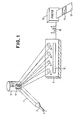
- FIG. 1 there is provided a schematic diagram of the conversion of an increment of optical information into an electrical signal employing the imaging device of the invention.
- FIG. 1 light 1 from a'source 2 is directed to an object 3 illustrated as a can and having thereon an information pattern 4 to be converted to an electrical signal.
- the pattern 4 is a schematic replica of a standard bar code for content and price information used in commerce and an iII ⁇ s- trative four segment portion thereof has the individual light elements thereof reflected so as to impinge the imaging device 5 embodying the invention.
- the device 5 there are photosensitive segments 6 through 9 and an output register 10 so that the light increments striking elements 6 through 9 are translated through the register element 10 into a pulse pattern signal 11 which is a replica of the bar code 4 and which in turn operates to drive a print mechanism 12 to produce on a tape 13 an ink configuration 14 corresponding to the elements of the pulse pattern 11 and of the bar code 4.
- Integrated optical-to-electrical transducers such as 5 in FIG. 1 that have been available heretofore in the art, have had two serious limitations.
- One is that the optical response of the transducer in the short wavelength end of the light spectrum operates to slow down the rate at which the information can be read out of the device where light levels are low.
- the second is that the devices have been using registers that are unduly complicated and large numbers of clocked phases were required to move the information in sequence.
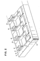
- FIG. 2 a three-dimensional illustration is provided of the integrated structure of the invention wherein the features are set forth in the integrated technology.
- gallium arsenide which is well known for its optical-electrical conversion properties and specific conductivity types are assigned:
- the layer 21 is also provided, in the portion for use as the charge-coupled device shift register, with a series of asymmetric impedance regions 27 which serve as barriers and operate to provide unidirectional charge transfer between the elements of the charge-coupled device register.
- the barriers 27 may be conveniently produced by ion implanting donors into the regions of the n-conductivity type gallium arsenide layer 21.
- FIG. 3 a further schematic is provided illustrating the metallized conductors that in response to a clock signal move the changes and an output and reset circuit.
- a bias metallization electrode 30 is provided which will be connected to a positive voltage and has fingers which make contact in the openings 26 to each of the photo-responsive elements.
- a barrier gate 31 is provided forming a thin metal Schottky barrier rectifying connection with each of the n-regions 21 and is shown as a stripe positioned perpendicular to the regions 21 adjacent to the photoelement region between the photoelement and the charge-coupled device region.
- a storage gate 32 again forming a metal Schottky barrier at each intersection with the layer 21, is next provided between the gate 31 and the charge-coupled device region.
- the barrier gate 31 and the storage gate 32 function in combination to even out the output and to permit integrating of the charge produced by the light that strikes the device elements.
- a transfer gate 33 is next provided, again forming a metal Schottky barrier at each intersection with the segments of the layer 21 and positioned between the storage gate 32 and the charge-coupled device so that upon a proper signal the charge stored in the storage region of the segment of the layer 21 associated with each phototransistor can be transferred to the charge-coupled array shift register.
- Clock eleectrodes 34 and 35 are provided for the charge movement in the shift register so that upon application of a signal the stored charge in the charge-coupled device segments provided by the cutouts 36 and 37 of the layer 21 are transferred as shown by the arrow 38 with back charge migration prevented by the implanted impedances 27.
- the output and reset capability is provided through a sensing electrode 46 connected to a circuit such that 2 FET transistor gate paths are provided in parallel.
- the output and reset circuit employs a voltage source 40 having one terminal connected to ground or common and having the opposite polarity terminal supplying potential to the drain electrode of reset transistor 41 and to the drain electrode of output transistor 42.
- the reset input signal is applied at the gate 43 of the reset transistor.
- the output is developed at electrode 44 across impedance 45 having the other terminal thereof connected to earth.
- the output 44 is connected to the source electrode of the output transistor, the gate thereof being connected to sensing electrode 46.
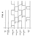
- FIG. 4 a timing chart is provided wherein the respective timing pulses assuming voltages of +13 Volts are illustrated.
- the bias gate 30 is shown connected to a steady state 0 Volts.
- the barrier gate 31 is connected at a positive level with respect to the substrate for example, 0.5 Volts.
- the signal at the storage gate 32 is shown increasing from zero to the 13 Volt level shown for the bias gate at intervals which are largely governed by the charge integration time of the photosensitive element.
- the signal on the transfer gate 33 increases from zero to the +13 Volts at a time when the integrated light generated charge on the storage gate has achieved a high level and remains long enough to transfer the energy into the transfer elements of the charge-coupled device.
- the clock gates 34 and 35, respectively, of the charge-coupled device are labelled Phase 1 and Phase 2.
- Phase 1 comes on at 13 V during the operation of the transfer gate and remains “on” until all charge is removed.
- Phase 2 comes “on” at the trailing part of Phase 1 and goes “off” with the rise of Phase 1.
- the signal on the reset 43, and so on sensing electrode 46 is shown as going from zero to 13 Volts at the end of each charge increment transfer.
- the optical-to-electrical transducer of the invention may be fabricated using well known semi- conductor integrated circuit manufacturing techniques such as vapour phase epitaxy, ion implantation and diffusion.
- the substrate 20 may be high resistivity chromium doped gallium arsenide formed through the technique of chemical vapour deposition.
- the n-region 21 may be epitaxially grown gallium arsenide with the doping level of around 10" tellurium donors per cc.
- the layer 21 could conveniently be about 1 micron deep over the entire substrate with growth prevented in the slots 37 and 38 by standard growth masking techniques or, alternatively, by growing over the entire substrate and using standard photolithographic and etching techniques.
- the p-type gallium arsenide layer 22 and the n+-type gallium arsenide layer 23 may be grown with a doping density of about 10 17 atoms/cc to a thickness of about 0.2 microns in the selected area desired by masking.
- the window of gallium aluminum arsenide 24 may be adjusted such that the aluminum quantity is 0.3 and the arsenic quantity is 0.7. With this layer 24 surface recombination is reduced and photoresponse is enhanced especially in the blue wavelength region.
- An alternative method of manufacture would be to grow all layers over the entire area and then by standard photolithographic masking and etching procedures the phototransistor array elements could be formed by etching out to the original n-region 21.
- a non- preferential etch such as the standard 40 parts hydrochloric acid, 1 part hydrogen peroxide and 1 part water can be used.
- a silicon dioxide passivation layer is then applied by chemical vapour deposition over the entire array and the gates 30 to 35 applied by standard metal evaporation techniques where the metal is AI or other well known Schottky gate metals and deposited about 300 ⁇ thick.
- optical-to-electrical transducer having gain and requiring only two clock phases.
- the optical-to-electrical transducer has light responsive electrical charge generation with electrical signal amplification, the capability to integrate the light generated signal to a selected magnitude and the ability to convert a plurality of individual signals into a serial electrical representation.
Landscapes
- Physics & Mathematics (AREA)
- Electromagnetism (AREA)
- Engineering & Computer Science (AREA)
- Health & Medical Sciences (AREA)
- General Health & Medical Sciences (AREA)
- Toxicology (AREA)
- Artificial Intelligence (AREA)
- Computer Vision & Pattern Recognition (AREA)
- General Physics & Mathematics (AREA)
- Theoretical Computer Science (AREA)
- Transforming Light Signals Into Electric Signals (AREA)
- Solid State Image Pick-Up Elements (AREA)
Applications Claiming Priority (2)
| Application Number | Priority Date | Filing Date | Title |
|---|---|---|---|
| US19155380A | 1980-09-29 | 1980-09-29 | |
| US191553 | 1980-09-29 |
Publications (3)
| Publication Number | Publication Date |
|---|---|
| EP0048805A2 EP0048805A2 (en) | 1982-04-07 |
| EP0048805A3 EP0048805A3 (en) | 1982-12-15 |
| EP0048805B1 true EP0048805B1 (en) | 1985-05-22 |
Family
ID=22705946
Family Applications (1)
| Application Number | Title | Priority Date | Filing Date |
|---|---|---|---|
| EP81106125A Expired EP0048805B1 (en) | 1980-09-29 | 1981-08-05 | Semiconductor integrated circuit optical image-to-electrical signal transducer |
Country Status (4)
| Country | Link |
|---|---|
| EP (1) | EP0048805B1 (enExample) |
| JP (1) | JPS5784689A (enExample) |
| CA (1) | CA1186784A (enExample) |
| DE (1) | DE3170600D1 (enExample) |
Families Citing this family (2)
| Publication number | Priority date | Publication date | Assignee | Title |
|---|---|---|---|---|
| EP0195339B1 (en) * | 1985-03-21 | 1992-07-29 | Abbott Laboratories | Spectrophotometer |
| JPH06215165A (ja) * | 1993-01-20 | 1994-08-05 | Matsushita Electric Ind Co Ltd | デジタル出力イメージセンサおよびそれを用いたバーコードリーダ |
Family Cites Families (7)
| Publication number | Priority date | Publication date | Assignee | Title |
|---|---|---|---|---|
| FR1500047A (fr) * | 1966-06-15 | 1967-11-03 | Comp Generale Electricite | Détecteur de lumière à semiconducteurs |
| US3909520A (en) * | 1969-10-14 | 1975-09-30 | Westinghouse Electric Corp | Readout system for a solid-state television camera |
| DE2440325A1 (de) * | 1974-08-22 | 1976-03-11 | Siemens Ag | Lichtempfindlicher transistor |
| JPS5255478A (en) * | 1975-10-31 | 1977-05-06 | Fujitsu Ltd | Charge transfer device |
| US4078243A (en) * | 1975-12-12 | 1978-03-07 | International Business Machines Corporation | Phototransistor array having uniform current response and method of manufacture |
| US4063268A (en) * | 1976-07-15 | 1977-12-13 | The United States Of America As Represented By The Secretary Of The Army | Silicon-polysilicon infrared image device with orientially etched detector |
| JPS5388518A (en) * | 1977-01-14 | 1978-08-04 | Sony Corp | Solid state pickup device |
-
1981
- 1981-08-05 EP EP81106125A patent/EP0048805B1/en not_active Expired
- 1981-08-05 DE DE8181106125T patent/DE3170600D1/de not_active Expired
- 1981-08-12 CA CA000383691A patent/CA1186784A/en not_active Expired
- 1981-09-14 JP JP56144084A patent/JPS5784689A/ja active Granted
Also Published As
| Publication number | Publication date |
|---|---|
| JPS6253108B2 (enExample) | 1987-11-09 |
| JPS5784689A (en) | 1982-05-27 |
| EP0048805A2 (en) | 1982-04-07 |
| EP0048805A3 (en) | 1982-12-15 |
| CA1186784A (en) | 1985-05-07 |
| DE3170600D1 (en) | 1985-06-27 |
Similar Documents
| Publication | Publication Date | Title |
|---|---|---|
| EP0165764B1 (en) | Depletion mode thin film semiconductor photodetectors | |
| CA1257922A (en) | Photoelectric converter | |
| US5200634A (en) | Thin film phototransistor and photosensor array using the same | |
| US4724470A (en) | Image sensor device having separate photosensor and charge storage | |
| US4866499A (en) | Photosensitive diode element and array | |
| JPH06500431A (ja) | フォトダイオードとccdエレメントとの間に転送ゲートを有するイメージセンサ | |
| US4258376A (en) | Charge coupled circuit arrangement using a punch-through charge introduction effect | |
| EP0361515B1 (en) | Thin film phototransistor and photosensor array using the same | |
| GB1576177A (en) | Phototransistors | |
| US4213137A (en) | Monolithic variable size detector | |
| JPH05211321A (ja) | アバランシェフォトダイオード、及びそれを具備する信号処理装置 | |
| US3842274A (en) | Photoconductively activated gated, infrared charge coupled imaging device (pagirccd) | |
| EP0283699B1 (en) | Photoelectric conversion device | |
| US4906856A (en) | Semiconductive photodetection device having coplanar circuit components | |
| US4488163A (en) | Highly isolated photodetectors | |
| US6020581A (en) | Solid state CMOS imager using silicon-on-insulator or bulk silicon | |
| EP0048805B1 (en) | Semiconductor integrated circuit optical image-to-electrical signal transducer | |
| CN214152901U (zh) | 一种垂直电荷转移型光子解调器 | |
| US5162885A (en) | Acoustic charge transport imager | |
| US4903103A (en) | Semiconductor photodiode device | |
| EP0494691A2 (en) | Photoelectric converting device and image processing apparatus utilizing the same | |
| EP0276683B1 (en) | Photoelectric conversion device | |
| US3633077A (en) | Semiconductor photoelectric converting device having spaced elements for decreasing surface recombination of minority carriers | |
| US3916429A (en) | Gated silicon diode array camera tube | |
| US3623027A (en) | Solid-state light-sensitive storage device |
Legal Events
| Date | Code | Title | Description |
|---|---|---|---|
| PUAI | Public reference made under article 153(3) epc to a published international application that has entered the european phase |
Free format text: ORIGINAL CODE: 0009012 |
|
| AK | Designated contracting states |
Designated state(s): DE FR GB IT |
|
| PUAL | Search report despatched |
Free format text: ORIGINAL CODE: 0009013 |
|
| AK | Designated contracting states |
Designated state(s): DE FR GB IT |
|
| 17P | Request for examination filed |
Effective date: 19821220 |
|
| GRAA | (expected) grant |
Free format text: ORIGINAL CODE: 0009210 |
|
| AK | Designated contracting states |
Designated state(s): DE FR GB IT |
|
| PG25 | Lapsed in a contracting state [announced via postgrant information from national office to epo] |
Ref country code: IT Free format text: LAPSE BECAUSE OF FAILURE TO SUBMIT A TRANSLATION OF THE DESCRIPTION OR TO PAY THE FEE WITHIN THE PRESCRIBED TIME-LIMIT;WARNING: LAPSES OF ITALIAN PATENTS WITH EFFECTIVE DATE BEFORE 2007 MAY HAVE OCCURRED AT ANY TIME BEFORE 2007. THE CORRECT EFFECTIVE DATE MAY BE DIFFERENT FROM THE ONE RECORDED. Effective date: 19850522 |
|
| REF | Corresponds to: |
Ref document number: 3170600 Country of ref document: DE Date of ref document: 19850627 |
|
| ET | Fr: translation filed | ||
| PLBE | No opposition filed within time limit |
Free format text: ORIGINAL CODE: 0009261 |
|
| STAA | Information on the status of an ep patent application or granted ep patent |
Free format text: STATUS: NO OPPOSITION FILED WITHIN TIME LIMIT |
|
| 26N | No opposition filed | ||
| PGFP | Annual fee paid to national office [announced via postgrant information from national office to epo] |
Ref country code: FR Payment date: 19900720 Year of fee payment: 10 |
|
| PGFP | Annual fee paid to national office [announced via postgrant information from national office to epo] |
Ref country code: GB Payment date: 19910717 Year of fee payment: 11 |
|
| PGFP | Annual fee paid to national office [announced via postgrant information from national office to epo] |
Ref country code: DE Payment date: 19910828 Year of fee payment: 11 |
|
| PG25 | Lapsed in a contracting state [announced via postgrant information from national office to epo] |
Ref country code: FR Effective date: 19920430 |
|
| REG | Reference to a national code |
Ref country code: FR Ref legal event code: ST |
|
| PG25 | Lapsed in a contracting state [announced via postgrant information from national office to epo] |
Ref country code: GB Effective date: 19920805 |
|
| GBPC | Gb: european patent ceased through non-payment of renewal fee |
Effective date: 19920805 |
|
| PG25 | Lapsed in a contracting state [announced via postgrant information from national office to epo] |
Ref country code: DE Effective date: 19930501 |