EP0045644B1 - Metallic contacts to compound semiconductor devices - Google Patents
Metallic contacts to compound semiconductor devices Download PDFInfo
- Publication number
- EP0045644B1 EP0045644B1 EP81303521A EP81303521A EP0045644B1 EP 0045644 B1 EP0045644 B1 EP 0045644B1 EP 81303521 A EP81303521 A EP 81303521A EP 81303521 A EP81303521 A EP 81303521A EP 0045644 B1 EP0045644 B1 EP 0045644B1
- Authority
- EP
- European Patent Office
- Prior art keywords
- metal layer
- contact
- metal
- semiconductor
- titanium
- Prior art date
- Legal status (The legal status is an assumption and is not a legal conclusion. Google has not performed a legal analysis and makes no representation as to the accuracy of the status listed.)
- Expired
Links
- 239000004065 semiconductor Substances 0.000 title claims description 55
- 150000001875 compounds Chemical class 0.000 title claims description 15
- 229910052751 metal Inorganic materials 0.000 claims description 98
- 239000002184 metal Substances 0.000 claims description 98
- 239000010936 titanium Substances 0.000 claims description 24
- 229910052719 titanium Inorganic materials 0.000 claims description 23
- RTAQQCXQSZGOHL-UHFFFAOYSA-N Titanium Chemical compound [Ti] RTAQQCXQSZGOHL-UHFFFAOYSA-N 0.000 claims description 22
- 239000010931 gold Substances 0.000 claims description 20
- 229910052737 gold Inorganic materials 0.000 claims description 20
- PCHJSUWPFVWCPO-UHFFFAOYSA-N gold Chemical compound [Au] PCHJSUWPFVWCPO-UHFFFAOYSA-N 0.000 claims description 18
- KDLHZDBZIXYQEI-UHFFFAOYSA-N Palladium Chemical compound [Pd] KDLHZDBZIXYQEI-UHFFFAOYSA-N 0.000 claims description 16
- PXHVJJICTQNCMI-UHFFFAOYSA-N Nickel Chemical compound [Ni] PXHVJJICTQNCMI-UHFFFAOYSA-N 0.000 claims description 10
- VYZAMTAEIAYCRO-UHFFFAOYSA-N Chromium Chemical compound [Cr] VYZAMTAEIAYCRO-UHFFFAOYSA-N 0.000 claims description 9
- 229910052804 chromium Inorganic materials 0.000 claims description 9
- 239000011651 chromium Substances 0.000 claims description 9
- 230000004888 barrier function Effects 0.000 claims description 8
- 238000009792 diffusion process Methods 0.000 claims description 8
- 229910052738 indium Inorganic materials 0.000 claims description 8
- APFVFJFRJDLVQX-UHFFFAOYSA-N indium atom Chemical compound [In] APFVFJFRJDLVQX-UHFFFAOYSA-N 0.000 claims description 8
- 239000000463 material Substances 0.000 claims description 8
- 150000002739 metals Chemical class 0.000 claims description 8
- 229910052763 palladium Inorganic materials 0.000 claims description 8
- WPYVAWXEWQSOGY-UHFFFAOYSA-N indium antimonide Chemical compound [Sb]#[In] WPYVAWXEWQSOGY-UHFFFAOYSA-N 0.000 claims description 7
- 229910052782 aluminium Inorganic materials 0.000 claims description 6
- XAGFODPZIPBFFR-UHFFFAOYSA-N aluminium Chemical compound [Al] XAGFODPZIPBFFR-UHFFFAOYSA-N 0.000 claims description 6
- UFHFLCQGNIYNRP-UHFFFAOYSA-N Hydrogen Chemical compound [H][H] UFHFLCQGNIYNRP-UHFFFAOYSA-N 0.000 claims description 5
- FYYHWMGAXLPEAU-UHFFFAOYSA-N Magnesium Chemical compound [Mg] FYYHWMGAXLPEAU-UHFFFAOYSA-N 0.000 claims description 5
- 229910052739 hydrogen Inorganic materials 0.000 claims description 5
- 239000001257 hydrogen Substances 0.000 claims description 5
- 229910052749 magnesium Inorganic materials 0.000 claims description 5
- 239000011777 magnesium Substances 0.000 claims description 5
- 229910052759 nickel Inorganic materials 0.000 claims description 5
- 229910001218 Gallium arsenide Inorganic materials 0.000 claims description 4
- JBRZTFJDHDCESZ-UHFFFAOYSA-N AsGa Chemical compound [As]#[Ga] JBRZTFJDHDCESZ-UHFFFAOYSA-N 0.000 claims description 3
- 229910000673 Indium arsenide Inorganic materials 0.000 claims description 3
- 229910052733 gallium Inorganic materials 0.000 claims description 3
- RPQDHPTXJYYUPQ-UHFFFAOYSA-N indium arsenide Chemical compound [In]#[As] RPQDHPTXJYYUPQ-UHFFFAOYSA-N 0.000 claims description 3
- 229910052758 niobium Inorganic materials 0.000 claims description 3
- 239000010955 niobium Substances 0.000 claims description 3
- GUCVJGMIXFAOAE-UHFFFAOYSA-N niobium atom Chemical compound [Nb] GUCVJGMIXFAOAE-UHFFFAOYSA-N 0.000 claims description 3
- 229910052715 tantalum Inorganic materials 0.000 claims description 3
- GUVRBAGPIYLISA-UHFFFAOYSA-N tantalum atom Chemical compound [Ta] GUVRBAGPIYLISA-UHFFFAOYSA-N 0.000 claims description 3
- 229910052718 tin Inorganic materials 0.000 claims description 3
- WFKWXMTUELFFGS-UHFFFAOYSA-N tungsten Chemical compound [W] WFKWXMTUELFFGS-UHFFFAOYSA-N 0.000 claims description 3
- 229910052721 tungsten Inorganic materials 0.000 claims description 3
- 239000010937 tungsten Substances 0.000 claims description 3
- 229910052720 vanadium Inorganic materials 0.000 claims description 3
- GPPXJZIENCGNKB-UHFFFAOYSA-N vanadium Chemical compound [V]#[V] GPPXJZIENCGNKB-UHFFFAOYSA-N 0.000 claims description 3
- 229920002120 photoresistant polymer Polymers 0.000 description 15
- 239000010408 film Substances 0.000 description 9
- 238000000034 method Methods 0.000 description 9
- 239000003792 electrolyte Substances 0.000 description 7
- 238000002161 passivation Methods 0.000 description 6
- 230000015572 biosynthetic process Effects 0.000 description 5
- 230000005684 electric field Effects 0.000 description 5
- 235000012431 wafers Nutrition 0.000 description 5
- 238000007743 anodising Methods 0.000 description 4
- 238000000151 deposition Methods 0.000 description 4
- 230000008021 deposition Effects 0.000 description 4
- 238000002048 anodisation reaction Methods 0.000 description 3
- 238000009826 distribution Methods 0.000 description 3
- 238000005566 electron beam evaporation Methods 0.000 description 3
- 238000001465 metallisation Methods 0.000 description 3
- 239000000243 solution Substances 0.000 description 3
- 239000000758 substrate Substances 0.000 description 3
- 238000003491 array Methods 0.000 description 2
- 238000005868 electrolysis reaction Methods 0.000 description 2
- 238000009713 electroplating Methods 0.000 description 2
- 238000004519 manufacturing process Methods 0.000 description 2
- 229910044991 metal oxide Inorganic materials 0.000 description 2
- 150000004706 metal oxides Chemical class 0.000 description 2
- 230000003647 oxidation Effects 0.000 description 2
- 238000007254 oxidation reaction Methods 0.000 description 2
- BASFCYQUMIYNBI-UHFFFAOYSA-N platinum Chemical compound [Pt] BASFCYQUMIYNBI-UHFFFAOYSA-N 0.000 description 2
- 238000012545 processing Methods 0.000 description 2
- 229910052594 sapphire Inorganic materials 0.000 description 2
- 239000010980 sapphire Substances 0.000 description 2
- -1 (Hg Chemical class 0.000 description 1
- 238000009825 accumulation Methods 0.000 description 1
- 239000003929 acidic solution Substances 0.000 description 1
- 230000002378 acidificating effect Effects 0.000 description 1
- 230000002411 adverse Effects 0.000 description 1
- 239000007864 aqueous solution Substances 0.000 description 1
- 239000003637 basic solution Substances 0.000 description 1
- 230000015556 catabolic process Effects 0.000 description 1
- 239000003518 caustics Substances 0.000 description 1
- 239000002800 charge carrier Substances 0.000 description 1
- 238000003486 chemical etching Methods 0.000 description 1
- 238000006731 degradation reaction Methods 0.000 description 1
- 238000013461 design Methods 0.000 description 1
- 238000010348 incorporation Methods 0.000 description 1
- 239000001995 intermetallic alloy Substances 0.000 description 1
- 238000007737 ion beam deposition Methods 0.000 description 1
- 238000005259 measurement Methods 0.000 description 1
- 230000001590 oxidative effect Effects 0.000 description 1
- 229910052697 platinum Inorganic materials 0.000 description 1
- 229910052709 silver Inorganic materials 0.000 description 1
- 238000004544 sputter deposition Methods 0.000 description 1
- 239000000126 substance Substances 0.000 description 1
- 238000002207 thermal evaporation Methods 0.000 description 1
- 239000010409 thin film Substances 0.000 description 1
- 238000012876 topography Methods 0.000 description 1
- 229910052723 transition metal Inorganic materials 0.000 description 1
- 150000003624 transition metals Chemical class 0.000 description 1
- 230000005641 tunneling Effects 0.000 description 1
- 238000001771 vacuum deposition Methods 0.000 description 1
- 238000007738 vacuum evaporation Methods 0.000 description 1
Images
Classifications
-
- H—ELECTRICITY
- H01—ELECTRIC ELEMENTS
- H01L—SEMICONDUCTOR DEVICES NOT COVERED BY CLASS H10
- H01L21/00—Processes or apparatus adapted for the manufacture or treatment of semiconductor or solid state devices or of parts thereof
- H01L21/02—Manufacture or treatment of semiconductor devices or of parts thereof
- H01L21/02104—Forming layers
- H01L21/02107—Forming insulating materials on a substrate
- H01L21/02109—Forming insulating materials on a substrate characterised by the type of layer, e.g. type of material, porous/non-porous, pre-cursors, mixtures or laminates
- H01L21/02112—Forming insulating materials on a substrate characterised by the type of layer, e.g. type of material, porous/non-porous, pre-cursors, mixtures or laminates characterised by the material of the layer
- H01L21/02172—Forming insulating materials on a substrate characterised by the type of layer, e.g. type of material, porous/non-porous, pre-cursors, mixtures or laminates characterised by the material of the layer the material containing at least one metal element, e.g. metal oxides, metal nitrides, metal oxynitrides or metal carbides
- H01L21/02175—Forming insulating materials on a substrate characterised by the type of layer, e.g. type of material, porous/non-porous, pre-cursors, mixtures or laminates characterised by the material of the layer the material containing at least one metal element, e.g. metal oxides, metal nitrides, metal oxynitrides or metal carbides characterised by the metal
- H01L21/02186—Forming insulating materials on a substrate characterised by the type of layer, e.g. type of material, porous/non-porous, pre-cursors, mixtures or laminates characterised by the material of the layer the material containing at least one metal element, e.g. metal oxides, metal nitrides, metal oxynitrides or metal carbides characterised by the metal the material containing titanium, e.g. TiO2
-
- H—ELECTRICITY
- H01—ELECTRIC ELEMENTS
- H01L—SEMICONDUCTOR DEVICES NOT COVERED BY CLASS H10
- H01L21/00—Processes or apparatus adapted for the manufacture or treatment of semiconductor or solid state devices or of parts thereof
- H01L21/02—Manufacture or treatment of semiconductor devices or of parts thereof
- H01L21/02104—Forming layers
- H01L21/02107—Forming insulating materials on a substrate
- H01L21/02225—Forming insulating materials on a substrate characterised by the process for the formation of the insulating layer
- H01L21/02227—Forming insulating materials on a substrate characterised by the process for the formation of the insulating layer formation by a process other than a deposition process
- H01L21/0223—Forming insulating materials on a substrate characterised by the process for the formation of the insulating layer formation by a process other than a deposition process formation by oxidation, e.g. oxidation of the substrate
- H01L21/02244—Forming insulating materials on a substrate characterised by the process for the formation of the insulating layer formation by a process other than a deposition process formation by oxidation, e.g. oxidation of the substrate of a metallic layer
-
- H—ELECTRICITY
- H01—ELECTRIC ELEMENTS
- H01L—SEMICONDUCTOR DEVICES NOT COVERED BY CLASS H10
- H01L21/00—Processes or apparatus adapted for the manufacture or treatment of semiconductor or solid state devices or of parts thereof
- H01L21/02—Manufacture or treatment of semiconductor devices or of parts thereof
- H01L21/02104—Forming layers
- H01L21/02107—Forming insulating materials on a substrate
- H01L21/02225—Forming insulating materials on a substrate characterised by the process for the formation of the insulating layer
- H01L21/02227—Forming insulating materials on a substrate characterised by the process for the formation of the insulating layer formation by a process other than a deposition process
- H01L21/02258—Forming insulating materials on a substrate characterised by the process for the formation of the insulating layer formation by a process other than a deposition process formation by anodic treatment, e.g. anodic oxidation
-
- H—ELECTRICITY
- H01—ELECTRIC ELEMENTS
- H01L—SEMICONDUCTOR DEVICES NOT COVERED BY CLASS H10
- H01L21/00—Processes or apparatus adapted for the manufacture or treatment of semiconductor or solid state devices or of parts thereof
- H01L21/02—Manufacture or treatment of semiconductor devices or of parts thereof
- H01L21/04—Manufacture or treatment of semiconductor devices or of parts thereof the devices having potential barriers, e.g. a PN junction, depletion layer or carrier concentration layer
- H01L21/18—Manufacture or treatment of semiconductor devices or of parts thereof the devices having potential barriers, e.g. a PN junction, depletion layer or carrier concentration layer the devices having semiconductor bodies comprising elements of Group IV of the Periodic Table or AIIIBV compounds with or without impurities, e.g. doping materials
- H01L21/28—Manufacture of electrodes on semiconductor bodies using processes or apparatus not provided for in groups H01L21/20 - H01L21/268
- H01L21/283—Deposition of conductive or insulating materials for electrodes conducting electric current
- H01L21/285—Deposition of conductive or insulating materials for electrodes conducting electric current from a gas or vapour, e.g. condensation
- H01L21/28506—Deposition of conductive or insulating materials for electrodes conducting electric current from a gas or vapour, e.g. condensation of conductive layers
- H01L21/28575—Deposition of conductive or insulating materials for electrodes conducting electric current from a gas or vapour, e.g. condensation of conductive layers on semiconductor bodies comprising AIIIBV compounds
-
- H—ELECTRICITY
- H01—ELECTRIC ELEMENTS
- H01L—SEMICONDUCTOR DEVICES NOT COVERED BY CLASS H10
- H01L21/00—Processes or apparatus adapted for the manufacture or treatment of semiconductor or solid state devices or of parts thereof
- H01L21/02—Manufacture or treatment of semiconductor devices or of parts thereof
- H01L21/04—Manufacture or treatment of semiconductor devices or of parts thereof the devices having potential barriers, e.g. a PN junction, depletion layer or carrier concentration layer
- H01L21/34—Manufacture or treatment of semiconductor devices or of parts thereof the devices having potential barriers, e.g. a PN junction, depletion layer or carrier concentration layer the devices having semiconductor bodies not provided for in groups H01L21/0405, H01L21/0445, H01L21/06, H01L21/16 and H01L21/18 with or without impurities, e.g. doping materials
- H01L21/44—Manufacture of electrodes on semiconductor bodies using processes or apparatus not provided for in groups H01L21/38 - H01L21/428
- H01L21/441—Deposition of conductive or insulating materials for electrodes
- H01L21/443—Deposition of conductive or insulating materials for electrodes from a gas or vapour, e.g. condensation
-
- H—ELECTRICITY
- H01—ELECTRIC ELEMENTS
- H01L—SEMICONDUCTOR DEVICES NOT COVERED BY CLASS H10
- H01L21/00—Processes or apparatus adapted for the manufacture or treatment of semiconductor or solid state devices or of parts thereof
- H01L21/02—Manufacture or treatment of semiconductor devices or of parts thereof
- H01L21/04—Manufacture or treatment of semiconductor devices or of parts thereof the devices having potential barriers, e.g. a PN junction, depletion layer or carrier concentration layer
- H01L21/34—Manufacture or treatment of semiconductor devices or of parts thereof the devices having potential barriers, e.g. a PN junction, depletion layer or carrier concentration layer the devices having semiconductor bodies not provided for in groups H01L21/0405, H01L21/0445, H01L21/06, H01L21/16 and H01L21/18 with or without impurities, e.g. doping materials
- H01L21/46—Treatment of semiconductor bodies using processes or apparatus not provided for in groups H01L21/428
- H01L21/461—Treatment of semiconductor bodies using processes or apparatus not provided for in groups H01L21/428 to change their surface-physical characteristics or shape, e.g. etching, polishing, cutting
- H01L21/469—Treatment of semiconductor bodies using processes or apparatus not provided for in groups H01L21/428 to change their surface-physical characteristics or shape, e.g. etching, polishing, cutting to form insulating layers thereon, e.g. for masking or by using photolithographic techniques; After-treatment of these layers
-
- H—ELECTRICITY
- H01—ELECTRIC ELEMENTS
- H01L—SEMICONDUCTOR DEVICES NOT COVERED BY CLASS H10
- H01L23/00—Details of semiconductor or other solid state devices
- H01L23/52—Arrangements for conducting electric current within the device in operation from one component to another, i.e. interconnections, e.g. wires, lead frames
- H01L23/522—Arrangements for conducting electric current within the device in operation from one component to another, i.e. interconnections, e.g. wires, lead frames including external interconnections consisting of a multilayer structure of conductive and insulating layers inseparably formed on the semiconductor body
- H01L23/532—Arrangements for conducting electric current within the device in operation from one component to another, i.e. interconnections, e.g. wires, lead frames including external interconnections consisting of a multilayer structure of conductive and insulating layers inseparably formed on the semiconductor body characterised by the materials
- H01L23/53204—Conductive materials
- H01L23/53209—Conductive materials based on metals, e.g. alloys, metal silicides
-
- H—ELECTRICITY
- H01—ELECTRIC ELEMENTS
- H01L—SEMICONDUCTOR DEVICES NOT COVERED BY CLASS H10
- H01L29/00—Semiconductor devices specially adapted for rectifying, amplifying, oscillating or switching and having potential barriers; Capacitors or resistors having potential barriers, e.g. a PN-junction depletion layer or carrier concentration layer; Details of semiconductor bodies or of electrodes thereof ; Multistep manufacturing processes therefor
- H01L29/40—Electrodes ; Multistep manufacturing processes therefor
- H01L29/43—Electrodes ; Multistep manufacturing processes therefor characterised by the materials of which they are formed
- H01L29/45—Ohmic electrodes
- H01L29/452—Ohmic electrodes on AIII-BV compounds
-
- H—ELECTRICITY
- H01—ELECTRIC ELEMENTS
- H01L—SEMICONDUCTOR DEVICES NOT COVERED BY CLASS H10
- H01L2924/00—Indexing scheme for arrangements or methods for connecting or disconnecting semiconductor or solid-state bodies as covered by H01L24/00
- H01L2924/0001—Technical content checked by a classifier
- H01L2924/0002—Not covered by any one of groups H01L24/00, H01L24/00 and H01L2224/00
Definitions
- This invention relates to metallic contacts to compound semiconductor devices, and, more particularly, to metallic contacts that are compatible with anodic formation of a native oxide used to passivate the semiconductor surface.
- Compound semiconductor devices include devices which are fabricated employing mixed valence semiconductor materials; examples include II-VI compounds, such as (Hg,Cd)Te, IV-VI compounds such as (Pb,Sn)Te, and III-V compounds such as GaAs, InAs, InSb, (In,Ga)Sb and ln(As,Sb). Typical devices include photoconductors and photodiodes.
- II-VI compounds such as (Hg,Cd)Te
- IV-VI compounds such as (Pb,Sn)Te
- III-V compounds such as GaAs, InAs, InSb, (In,Ga)Sb and ln(As,Sb).
- Typical devices include photoconductors and photodiodes.
- a non-oxidizing top contact metal such as gold
- a rapidly diffusing metal such as indium.
- a native oxide would be anodically grown to passivate exposed portions of the semiconductor surface.
- Such non-uniform oxide thickness causes variation in the degree of accumulation or depletion of charge at the interface between the semiconductor and oxide, thus causing non-uniformity in the electrical characteristics of the device.
- the gold is also electrochemically attacked and often etched away during the anodization process, thereby yielding oversized devices and/or a rectifying junction at the interface between the active area of the device and the contact metal.
- indium will diffuse into and eventually destroy certain devices, such as those employing (Hg,Cd)Te.
- IBM Technical Disclosure Bulletin, Vol. 21, No. 4, Sept. 1978, Page 1753 discloses that incorporation of a layer of a transition metal between a conductive contact such as Ag or Au, and a GaAs semiconductor will provide a thermal barrier to diffusion and reduce degradation of the junction during subsequent processing or under device operating conditions where temperatures can reach 350°C.
- a semiconductor device comprising a compound semiconductor material, which is anodically oxidizable to form a passivating native oxide on exposed surfaces, includes a metallic contact comprising a contact metal layer formed on a portion of the semiconductor surface, the contact metal layer forming a substantially non-rectifying contact with the semiconductor surface and providing a diffusion barrier to the atoms of metal layers deposited over the contact metal layer characterised in that an oxidizable metal layer is formed covering the entire top surface of the contact metal layer, the oxidizable metal selected from the group consisting of metals occupying a position between hydrogen and magnesium in the Electromotive Series. Following formation of the metal contact, exposed surfaces of the semiconductor material are then passivated by anodically forming a native oxide thereon.
- the top metal layer forms an insulating oxide when the semiconductor device is placed in an electrolytic anodizing solution to passivate exposed semiconductor surfaces. Oxide and device non-uniformities inherent with previously used metallic contact systems are eliminated, since the oxidized metal will not continue to conduct current. Thus, the electric field distribution in the electrolyte will not be disrupted by the presence of the metal.
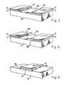
- Figs. 1-3 depict problems associated with various attempts in the prior art to form metallic contacts 11 on the surface of a semiconductor 10 and to passivate exposed semiconductor surfaces, e.g., 10a.
- a simple photodetector is depicted, the active device lying in the area between the two contacts.
- a native oxide on a compound semiconductor surface after metallic contacts have been applied has presented two problems. As shown in Fig. 1, a photoresist film 12 is processed to expose some of the contact metal 11 to ensure that the total device surface 10a is passivated.
- exposed metal portions 11a will distort or short out the electric field in the electrolyte (not shown) near the metal interface, causing non-uniform oxide growth and electrochemical attack of the metal.
- the exposed metal portions are completely etched away, yielding an oversized device-sensitive area and a rectifying junction between the device and its electrode.
- the anodically grown oxide is highly soluble in most basic or acidic solutions, it is not possible to anodize the device before metallization, because the semiconductor oxide would be undercut by many photoresist developers and metal etchants subsequently used to define the location of the contact metal.
- This condition is shown in Fig. 3, in which the exposed edges 13a, 13b of passivating oxide 13 are susceptible to chemical attack by caustic photoresist developers employed in defining photoresist film 12 and acidic etchants employed in defining subsequently deposited metal contacts (not shown).
- a metallic contact for use on compound semiconductor devices such as (Hg,Cd)Te and InSb that is compatible with a grown native oxide used to passivate semiconductor surfaces.
- the metallic contact comprises (a) a contact metal layer formed on a portion of a semiconductor surface, the contact metal layer forming a substantially non-rectifying contact with the semiconductor surface and providing a diffusion barrier and (b) an oxidizable metal layer on the contact metal layer which is selected from the group consisting of metals occupying a position between hydrogen and magnesium in the Electromotive Series.
- a suitable diffusion barrier metal include titanium, chromium and palladium
- examples of a suitable oxidizable metal include titanium, chromium, aluminum and indium.
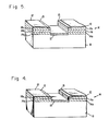
- metal contact 14 comprising at least two layers 14a and 14c.
- Layer 14a is a metal such as titanium, chromium or palladium and acts as a diffusion barrier to metals such as gold or indium which would otherwise adversely dope the semiconductor.
- Layer 14c is a metal such as aluminum, indium, titanium or chromium which oxidizes rapidly to form oxide layer 15 when exposed to an electrolytic anodizing solution (not shown). Therefore, the portion of the metal not covered with photoresist film 12 ceases to disrupt the electric field distribution in the electrolyte, and oxide 13 of substantially uniform thickness is formed. Also, the contact metal is not etched by the electrolyte, so device geometry and contact integrity are maintained.
- an intermediate metal layer 14b (shown in Fig. 5) such as gold may be used to provide a low resistance current path. The purity of all metal layers is that employed in normal commercial practice.
- the metallic contact of the invention is useful in a variety of semiconductor devices, including the fabrication of photoconductive (Hg,Cd)Te infrared detectors.
- the metallic contact of the invention provides improved yield and performance and reduced low-frequency noise by eliminating electrochemical attack of the metallic contact at the interface with the detector element. It also improves element-to-element uniformity because of the more uniform passivating oxide thickness obtained.
- the semiconductor materials to which the invention applies are compound semiconductors, especially those of classes II-VI, IV-VI and III-V; examples of such compound semiconductors include (Hg,Cd)Te, (Pb,Sn)Te, GaAs, InAs, InSb, (In,Ga)Sb and ln(As,Sb).
- the compound semiconductors which are advantageously employed in the practice of the invention are those which are anodically oxidizable to form a passivating native oxide layer on exposed surfaces. Such anodic oxidation employs procedures well-known in the art.
- the first metal layer, contact metal layer 14a, is directly in contact with the semiconductor surface; this layer provides a diffusion barrier to subsequently deposited metals and forms a substantially non-rectifying junction with the semiconductor surface.
- the non-rectifying junction ensures low noise and may be either truly ohmic or non-rectifying in the sense that conduction bands due to differences in work functions of the respective materials (metal and semiconductor) are bent upon contacting the semiconductor with metal such that tunneling of charge carriers can readily occur.
- the specific contact metal employed may differ from one compound semiconductor to another, so long as the metal possesses the foregoing properties.
- a suitable contact metal comprises a metal selected from the group consisting of titanium, chromium, nickel and palladium
- a suitable contact metal comprises a metal selected from the group consisting of titanium and palladium.
- titanium and palladium are preferred, since they provide the lowest contact noise and good adhesion to the semiconductor surface.
- Contact metal layer 14a may be deposited by any number of procedures employing process parameters well-known in the prior art, and the deposition of this layer does not form a part of this invention.
- it may be deposited by vacuum evaporation such as electron beam evaporation or RF or DC sputtering or thermal evaporation.
- it may be electroplated; for example, palladium may be electroplated on (Hg,Cd)Te and InSb.
- Yet another procedure includes ion beam deposition.
- Metal layer 14b is optional and may be employed to form a low resistance contact, such as required for 50 OlD Hg 8o Cd 2 ,Te photoconductors.
- a low resistance contact such as required for 50 OlD Hg 8o Cd 2 ,Te photoconductors.
- the first layer 14a is thin and typically has a high resistivity (e.g., in the case of titanium), then a lower resistivity would be required, which is provided by layer 14b of low resistivity metal.
- layer 14b may be used in those situations when the topography of the device is other than planar (e.g., mesa). For example, bonding contact wires directly to (Hg,Cd)Te devices formed on sapphire substrates is difficult, since the (Hg,Cd)Te is soft.
- a contact path extends across the surface of the semiconductor island, down one side and to an exposed surface of the sapphire substrate. Contact is accordingly made by wire bonding to metal supported on the harder substrate.
- a thin layer 14a could not maintain integrity under such topological contouring, and, accordingly, a thicker, low resistivity layer 14b would be suitably employed.
- a metal used for layer 14b has low resistance, physical stability (i.e., no whisker growth and no phase changes during processing) and no intermetallic alloy formation to other metals (layers 14a and 14c) which could form brittle products. That is, the low resistivity layer must be substantially metallurgically compatible with the contact metal and the oxidizable metal. Further, metal 14b should evidence good adhesion to the underlying metal 14a, be ductile and facilitate lead attachment. Gold and lead are metals that are advantageously employed as optional intermediate layer 14b; gold is preferred because of its compatability with contacting to external circuitry.
- the thickness of layer 14b ranges from about 1,000 to 20,000 ⁇ ; the particular thickness depends on specific device design. Factors influencing thickness include the final required resistance (the lower the required resistance, the thicker the metal layer), topology (the higher the contour, the thicker the layer), and device geometry (the closer the spacing, the thinner the layer). For example, for typical (Hg,Cd)Te photoconductors, gold ranging in thickness from about 15,000 to 20,000 A is preferably employed, while for typical InSb diodes, gold having a thickness of about 5,000 A is preferably employed.
- Layer 14b may be formed employing the same processes as layer 14a. However, in situations where comparatively thick films are desired, a thin film may first be evaporated, followed by electroplating to form thicker films for cost effectiveness.
- Metal layer 14c is one that is easily oxidizable, and lies above hydrogen (E>0.00 V) and below magnesium (E ⁇ 2.37 V) on the Electromotive Series. Since exposed portions of this metal layer are oxidized during passivation by electrolysis, then it must lie above hydrogen; otherwise, it will not oxidize. On the other hand, if the metal lies above magnesium, it will either oxidize too rapidly and be consumed during electrolysis or oxidize in air, forming a powdery compound.
- suitable metals include aluminum, titanium, nickel, chromium, indium, niobium, tantalum, tungsten and vanadium. Because of intermetallic formation with gold, indium and aluminum may not be desirable in certain applications. Titanium is especially preferred, since it is convenient in a metallic contact comprising Ti-Au-Ti wherein only two sources (Ti and Au) are required for vacuum deposition and etchants are readily available to selectively etch titanium but not gold for contact definition.
- the thickness of layer 14c ranges from about 500 to 1,000 A. If the layer is too thin, the electrolytic process etches through before the metal is adequately oxidized, while if the layer is too thick, internal stresses form during deposition which cause subsequent peeling of the layer. Preferably, the thickness of layer 14c ranges from about 600 to 800 A.
- Layer 14c may be deposited by any of the processes mentioned above in connection with layer 14a.
- a platinum cathode is usually employed in anodic oxidation, with anodic contact being made through the metallic contact 14 to the semiconductor; typically, aluminum wire is connected to the metallic contact.
- a metal oxide 15 is formed on portions of the surface of metal layer 14c exposed by a photoresist film 12. Once the metal oxide is formed, then the semiconductor oxide 13 is formed over the exposed surfaces of the semiconductor 10 to passivate them.
- portions of layer 14c are removed (not shown); usually these are removed in the contact bonding area only. Removal is conveniently done by chemical etching.
- a photoresist film is deposited over the semiconductor surface, including the detector sensitive areas.
- the photoresist film is processed to expose that portion of the semiconductor surface onto which metallic contacts of the invention are to be deposited.
- metallic contacts of the invention are to be deposited.
- titanium, gold and titanium within the described thickness ranges are evaporated over the entire photoresist-covered semiconductor surface.
- the photoresist is then lifted off, removing metal everywhere except in the contact areas.
- a second photoresist is then applied over the semiconductor surface, including metal contact areas, which is then processed to expose only the detector elements plus a small portion on each side.
- the detector sensitive areas are then anodically passivated.
- the photoresist mask is removed.
- a third photoresist mask is applied and processed which exposes the bonding areas, formed on a portion of the contacts. Portions of the top layer (e.g., titanium) are etched away, leaving exposed portions of the underlying low resistive contact (e.g., gold), ready for subsequent wire bonding thereto or electroplating thereof.
- devices having a metallic contact in accordance with the invention evidenced lower noise and an improved signal-to-noise ratio over those devices having a metallic contact outside the scope of the invention.
Landscapes
- Engineering & Computer Science (AREA)
- Microelectronics & Electronic Packaging (AREA)
- Power Engineering (AREA)
- Physics & Mathematics (AREA)
- Condensed Matter Physics & Semiconductors (AREA)
- General Physics & Mathematics (AREA)
- Computer Hardware Design (AREA)
- Manufacturing & Machinery (AREA)
- Ceramic Engineering (AREA)
- Electrodes Of Semiconductors (AREA)
- Formation Of Insulating Films (AREA)
- Light Receiving Elements (AREA)
Description
- This invention relates to metallic contacts to compound semiconductor devices, and, more particularly, to metallic contacts that are compatible with anodic formation of a native oxide used to passivate the semiconductor surface.
- Compound semiconductor devices include devices which are fabricated employing mixed valence semiconductor materials; examples include II-VI compounds, such as (Hg,Cd)Te, IV-VI compounds such as (Pb,Sn)Te, and III-V compounds such as GaAs, InAs, InSb, (In,Ga)Sb and ln(As,Sb). Typical devices include photoconductors and photodiodes.
- Such devices made in the past utilized either a non-oxidizing top contact metal such as gold or a rapidly diffusing metal such as indium. Following such metallization, a native oxide would be anodically grown to passivate exposed portions of the semiconductor surface. Use of the foregoing metallic contacts present many problems. For example, gold distorts or shorts out the electric field in the anodizing electrolyte, thereby causing non-uniform oxide thickness. Such non-uniform oxide thickness causes variation in the degree of accumulation or depletion of charge at the interface between the semiconductor and oxide, thus causing non-uniformity in the electrical characteristics of the device. The gold is also electrochemically attacked and often etched away during the anodization process, thereby yielding oversized devices and/or a rectifying junction at the interface between the active area of the device and the contact metal. On the other hand, it is known that indium will diffuse into and eventually destroy certain devices, such as those employing (Hg,Cd)Te.
- IBM Technical Disclosure Bulletin, Vol. 21, No. 4, Sept. 1978, Page 1753 discloses that incorporation of a layer of a transition metal between a conductive contact such as Ag or Au, and a GaAs semiconductor will provide a thermal barrier to diffusion and reduce degradation of the junction during subsequent processing or under device operating conditions where temperatures can reach 350°C.
- In accordance with the invention, a semiconductor device comprising a compound semiconductor material, which is anodically oxidizable to form a passivating native oxide on exposed surfaces, includes a metallic contact comprising a contact metal layer formed on a portion of the semiconductor surface, the contact metal layer forming a substantially non-rectifying contact with the semiconductor surface and providing a diffusion barrier to the atoms of metal layers deposited over the contact metal layer characterised in that an oxidizable metal layer is formed covering the entire top surface of the contact metal layer, the oxidizable metal selected from the group consisting of metals occupying a position between hydrogen and magnesium in the Electromotive Series. Following formation of the metal contact, exposed surfaces of the semiconductor material are then passivated by anodically forming a native oxide thereon.
- As a consequence of the metallic contact configuration of the invention, the top metal layer forms an insulating oxide when the semiconductor device is placed in an electrolytic anodizing solution to passivate exposed semiconductor surfaces. Oxide and device non-uniformities inherent with previously used metallic contact systems are eliminated, since the oxidized metal will not continue to conduct current. Thus, the electric field distribution in the electrolyte will not be disrupted by the presence of the metal.
-
- Fig. 1 is a perspective view, partly in section, of a metallic contact partially exposed by a photoresist mask to a passivating electrolyte in accordance with the prior art;
- Fig. 2 is a perspective view, partly in section, of a photoresist mask extending over the metallic contact/semiconductor interface in accordance with the prior art;
- Fig. 3 is a perspective view, partly in section, depicting anodization prior to metallization in accordance with the prior art;
- Fig. 4 is a perspective view, partly in section, depicting the multilayer metallic contact of the invention, which allows uniform passivation of semiconductor surfaces; and
- Fig. 5 is a perspective view, partly in section, depicting an alternate embodiment of the invention.
- Figs. 1-3 depict problems associated with various attempts in the prior art to form
metallic contacts 11 on the surface of asemiconductor 10 and to passivate exposed semiconductor surfaces, e.g., 10a. Here, a simple photodetector is depicted, the active device lying in the area between the two contacts. Historically, forming a native oxide on a compound semiconductor surface after metallic contacts have been applied has presented two problems. As shown in Fig. 1, aphotoresist film 12 is processed to expose some of thecontact metal 11 to ensure that the total device surface 10a is passivated. During anodic passivation, exposed metal portions 11a will distort or short out the electric field in the electrolyte (not shown) near the metal interface, causing non-uniform oxide growth and electrochemical attack of the metal. In some cases, the exposed metal portions are completely etched away, yielding an oversized device-sensitive area and a rectifying junction between the device and its electrode. - Alternately, as shown in Fig. 2, if the
photoresist film 12 completely covers themetal 11, it must also cover asmall part 10b of the semiconductor surface, thereby leaving part of the device un- passivated. This condition is also unacceptable, as it often yields a noisy, rectifying junction in series with the contact. - Since the anodically grown oxide is highly soluble in most basic or acidic solutions, it is not possible to anodize the device before metallization, because the semiconductor oxide would be undercut by many photoresist developers and metal etchants subsequently used to define the location of the contact metal. This condition is shown in Fig. 3, in which the exposed
edges 13a, 13b of passivatingoxide 13 are susceptible to chemical attack by caustic photoresist developers employed in definingphotoresist film 12 and acidic etchants employed in defining subsequently deposited metal contacts (not shown). - In accordance with the invention, a metallic contact for use on compound semiconductor devices such as (Hg,Cd)Te and InSb that is compatible with a grown native oxide used to passivate semiconductor surfaces is provided. The metallic contact comprises (a) a contact metal layer formed on a portion of a semiconductor surface, the contact metal layer forming a substantially non-rectifying contact with the semiconductor surface and providing a diffusion barrier and (b) an oxidizable metal layer on the contact metal layer which is selected from the group consisting of metals occupying a position between hydrogen and magnesium in the Electromotive Series. Examples of a suitable diffusion barrier metal include titanium, chromium and palladium, while examples of a suitable oxidizable metal include titanium, chromium, aluminum and indium. When placed in an electrolytic anodizing solution, the top layer forms an insulating oxide so that it will not continue to conduct current and disrupt the electric field distribution in the electrolyte. Consequently, oxide non-uniformities inherent with prior art contact systems are eliminated.
- As shown in Figs. 4 and 5, contact to
semiconductor 10 is made throughmetal contact 14 comprising at least twolayers 14a and 14c. Layer 14a is a metal such as titanium, chromium or palladium and acts as a diffusion barrier to metals such as gold or indium which would otherwise adversely dope the semiconductor.Layer 14c is a metal such as aluminum, indium, titanium or chromium which oxidizes rapidly to formoxide layer 15 when exposed to an electrolytic anodizing solution (not shown). Therefore, the portion of the metal not covered withphotoresist film 12 ceases to disrupt the electric field distribution in the electrolyte, andoxide 13 of substantially uniform thickness is formed. Also, the contact metal is not etched by the electrolyte, so device geometry and contact integrity are maintained. If desired, anintermediate metal layer 14b (shown in Fig. 5) such as gold may be used to provide a low resistance current path. The purity of all metal layers is that employed in normal commercial practice. - The metallic contact of the invention is useful in a variety of semiconductor devices, including the fabrication of photoconductive (Hg,Cd)Te infrared detectors. The metallic contact of the invention provides improved yield and performance and reduced low-frequency noise by eliminating electrochemical attack of the metallic contact at the interface with the detector element. It also improves element-to-element uniformity because of the more uniform passivating oxide thickness obtained.
- The semiconductor materials to which the invention applies are compound semiconductors, especially those of classes II-VI, IV-VI and III-V; examples of such compound semiconductors include (Hg,Cd)Te, (Pb,Sn)Te, GaAs, InAs, InSb, (In,Ga)Sb and ln(As,Sb). The compound semiconductors which are advantageously employed in the practice of the invention are those which are anodically oxidizable to form a passivating native oxide layer on exposed surfaces. Such anodic oxidation employs procedures well-known in the art.
- The first metal layer, contact metal layer 14a, is directly in contact with the semiconductor surface; this layer provides a diffusion barrier to subsequently deposited metals and forms a substantially non-rectifying junction with the semiconductor surface. The non-rectifying junction ensures low noise and may be either truly ohmic or non-rectifying in the sense that conduction bands due to differences in work functions of the respective materials (metal and semiconductor) are bent upon contacting the semiconductor with metal such that tunneling of charge carriers can readily occur. The specific contact metal employed may differ from one compound semiconductor to another, so long as the metal possesses the foregoing properties. In the case of (Hg,Cd)Te, a suitable contact metal comprises a metal selected from the group consisting of titanium, chromium, nickel and palladium, while in the case of InSb, a suitable contact metal comprises a metal selected from the group consisting of titanium and palladium. For (Hg,Cd)Te, titanium and palladium are preferred, since they provide the lowest contact noise and good adhesion to the semiconductor surface.
- The thickness of contact metal layer 14a ranges from about 300 to 1,000 A (1 Å=0.1 nm). If the metal layer is substantially less than about 300 A, then it will not form an adequate diffusion barrier, while if it is considerably thicker than about 1,000 A, then internal stresses are generated during deposition which cause subsequent peeling of the metal layer. Preferably, the thickness of contact metal layer 14a ranges from about 600 to 800 A.
- Contact metal layer 14a may be deposited by any number of procedures employing process parameters well-known in the prior art, and the deposition of this layer does not form a part of this invention. For example, it may be deposited by vacuum evaporation such as electron beam evaporation or RF or DC sputtering or thermal evaporation. Alternatively, it may be electroplated; for example, palladium may be electroplated on (Hg,Cd)Te and InSb. Yet another procedure includes ion beam deposition.
-
Metal layer 14b is optional and may be employed to form a low resistance contact, such as required for 50 OlD Hg8oCd2,Te photoconductors. In such a case, since the first layer 14a is thin and typically has a high resistivity (e.g., in the case of titanium), then a lower resistivity would be required, which is provided bylayer 14b of low resistivity metal. Alternatively,layer 14b may be used in those situations when the topography of the device is other than planar (e.g., mesa). For example, bonding contact wires directly to (Hg,Cd)Te devices formed on sapphire substrates is difficult, since the (Hg,Cd)Te is soft. In such cases, a contact path extends across the surface of the semiconductor island, down one side and to an exposed surface of the sapphire substrate. Contact is accordingly made by wire bonding to metal supported on the harder substrate. A thin layer 14a could not maintain integrity under such topological contouring, and, accordingly, a thicker,low resistivity layer 14b would be suitably employed. - The characteristics of a metal used for
layer 14b is that it have low resistance, physical stability (i.e., no whisker growth and no phase changes during processing) and no intermetallic alloy formation to other metals (layers 14a and 14c) which could form brittle products. That is, the low resistivity layer must be substantially metallurgically compatible with the contact metal and the oxidizable metal. Further,metal 14b should evidence good adhesion to the underlying metal 14a, be ductile and facilitate lead attachment. Gold and lead are metals that are advantageously employed as optionalintermediate layer 14b; gold is preferred because of its compatability with contacting to external circuitry. - The thickness of
layer 14b ranges from about 1,000 to 20,000 Å; the particular thickness depends on specific device design. Factors influencing thickness include the final required resistance (the lower the required resistance, the thicker the metal layer), topology (the higher the contour, the thicker the layer), and device geometry (the closer the spacing, the thinner the layer). For example, for typical (Hg,Cd)Te photoconductors, gold ranging in thickness from about 15,000 to 20,000 A is preferably employed, while for typical InSb diodes, gold having a thickness of about 5,000 A is preferably employed. -
Layer 14b may be formed employing the same processes as layer 14a. However, in situations where comparatively thick films are desired, a thin film may first be evaporated, followed by electroplating to form thicker films for cost effectiveness. -
Metal layer 14c is one that is easily oxidizable, and lies above hydrogen (E>0.00 V) and below magnesium (E<2.37 V) on the Electromotive Series. Since exposed portions of this metal layer are oxidized during passivation by electrolysis, then it must lie above hydrogen; otherwise, it will not oxidize. On the other hand, if the metal lies above magnesium, it will either oxidize too rapidly and be consumed during electrolysis or oxidize in air, forming a powdery compound. Examples of suitable metals include aluminum, titanium, nickel, chromium, indium, niobium, tantalum, tungsten and vanadium. Because of intermetallic formation with gold, indium and aluminum may not be desirable in certain applications. Titanium is especially preferred, since it is convenient in a metallic contact comprising Ti-Au-Ti wherein only two sources (Ti and Au) are required for vacuum deposition and etchants are readily available to selectively etch titanium but not gold for contact definition. - The thickness of
layer 14c ranges from about 500 to 1,000 A. If the layer is too thin, the electrolytic process etches through before the metal is adequately oxidized, while if the layer is too thick, internal stresses form during deposition which cause subsequent peeling of the layer. Preferably, the thickness oflayer 14c ranges from about 600 to 800 A. -
Layer 14c may be deposited by any of the processes mentioned above in connection with layer 14a. - Following deposition of
metallic contact 14, exposed surfaces of the semiconductor are then passivated by forming anative oxide 13 thereon. This passivation is performed anodically in an aqueous solution. There are many variations of the specific process parameters employed during anodization, and these are well-known in the prior art. - A platinum cathode is usually employed in anodic oxidation, with anodic contact being made through the
metallic contact 14 to the semiconductor; typically, aluminum wire is connected to the metallic contact. During the course of passivation, ametal oxide 15 is formed on portions of the surface ofmetal layer 14c exposed by aphotoresist film 12. Once the metal oxide is formed, then thesemiconductor oxide 13 is formed over the exposed surfaces of thesemiconductor 10 to passivate them. - Following passivation, portions of
layer 14c are removed (not shown); usually these are removed in the contact bonding area only. Removal is conveniently done by chemical etching. - In the fabrication of a typical semiconductor detector having already formed thereon detector sensitive areas, a photoresist film is deposited over the semiconductor surface, including the detector sensitive areas. The photoresist film is processed to expose that portion of the semiconductor surface onto which metallic contacts of the invention are to be deposited. In the preferred embodiment employing (Hg,Cd)Te devices, titanium, gold and titanium within the described thickness ranges are evaporated over the entire photoresist-covered semiconductor surface. The photoresist is then lifted off, removing metal everywhere except in the contact areas. A second photoresist is then applied over the semiconductor surface, including metal contact areas, which is then processed to expose only the detector elements plus a small portion on each side. This "picture frame" around each element is typically about 0.2 to 0.3 mils (1 mil=2.54×10⁻⁵ m) extra and ensures that the detector elements will be completely passivated. The detector sensitive areas are then anodically passivated. The photoresist mask is removed. A third photoresist mask is applied and processed which exposes the bonding areas, formed on a portion of the contacts. Portions of the top layer (e.g., titanium) are etched away, leaving exposed portions of the underlying low resistive contact (e.g., gold), ready for subsequent wire bonding thereto or electroplating thereof.
- From the same boule of 0.1 eV HgaaCd2oTe, adjacent wafers were processed to form photoconductors comprising linear arrays of 2x2 mil elements, with 200 elements per array and six arrays per wafer. On one wafer, a three layer metallic contact comprising 700 A titanium, 15,000 A gold and 500 A titanium, all deposited by electron beam evaporation, was formed. On the other wafer, a two layer metallic contact comprising 700 A titanium and 15,000 A gold, also deposited by electron beam evaporation, was formed. The only difference was the formation of an easily oxidizable metal layer on the first wafer. The following properties were measured at 77°K: resistance R in ohms, noise N in nV/Hz1/2, responsivity Rv in 103 V/Watt and signal-to-noise ratio D*in cm-Hz1/2/Watt. These measurements are listed in the Table below; the data associated with each sample listed represent average results of a 200 element array.

- As seen from an examination of the Table, devices having a metallic contact in accordance with the invention evidenced lower noise and an improved signal-to-noise ratio over those devices having a metallic contact outside the scope of the invention.
Claims (8)
Applications Claiming Priority (2)
| Application Number | Priority Date | Filing Date | Title |
|---|---|---|---|
| US17496380A | 1980-08-04 | 1980-08-04 | |
| US174963 | 1980-08-04 |
Publications (3)
| Publication Number | Publication Date |
|---|---|
| EP0045644A2 EP0045644A2 (en) | 1982-02-10 |
| EP0045644A3 EP0045644A3 (en) | 1984-02-08 |
| EP0045644B1 true EP0045644B1 (en) | 1987-03-18 |
Family
ID=22638251
Family Applications (1)
| Application Number | Title | Priority Date | Filing Date |
|---|---|---|---|
| EP81303521A Expired EP0045644B1 (en) | 1980-08-04 | 1981-07-31 | Metallic contacts to compound semiconductor devices |
Country Status (3)
| Country | Link |
|---|---|
| EP (1) | EP0045644B1 (en) |
| JP (1) | JPH0258787B2 (en) |
| DE (1) | DE3176025D1 (en) |
Families Citing this family (5)
| Publication number | Priority date | Publication date | Assignee | Title |
|---|---|---|---|---|
| JPS5954228A (en) * | 1982-09-22 | 1984-03-29 | Toshiba Corp | Anodic oxidation method for compound semiconductor |
| JPS60249337A (en) * | 1984-05-24 | 1985-12-10 | Fujitsu Ltd | Manufacture of semiconductor device |
| JPS6467964A (en) * | 1987-09-08 | 1989-03-14 | Mitsubishi Electric Corp | Multilayer electrode structure |
| JP3278951B2 (en) * | 1992-10-23 | 2002-04-30 | ソニー株式会社 | Method of forming ohmic electrode |
| JP2009206357A (en) * | 2008-02-28 | 2009-09-10 | Asahi Kasei Electronics Co Ltd | Compound semiconductor device and method for manufacturing compound semiconductor device |
Family Cites Families (3)
| Publication number | Priority date | Publication date | Assignee | Title |
|---|---|---|---|---|
| GB1469953A (en) * | 1973-05-18 | 1977-04-14 | Philips Electronic Associated | Semiconductor devices |
| JPS5141473A (en) * | 1974-10-01 | 1976-04-07 | Berumanto Futsuzu Nv | Merengeseihin oyobi sonoruijibutsu |
| US4000508A (en) * | 1975-07-17 | 1976-12-28 | Honeywell Inc. | Ohmic contacts to p-type mercury cadmium telluride |
-
1981
- 1981-07-31 DE DE8181303521T patent/DE3176025D1/en not_active Expired
- 1981-07-31 EP EP81303521A patent/EP0045644B1/en not_active Expired
- 1981-08-04 JP JP56122353A patent/JPH0258787B2/ja not_active Expired - Lifetime
Also Published As
| Publication number | Publication date |
|---|---|
| EP0045644A2 (en) | 1982-02-10 |
| JPS5753932A (en) | 1982-03-31 |
| JPH0258787B2 (en) | 1990-12-10 |
| EP0045644A3 (en) | 1984-02-08 |
| DE3176025D1 (en) | 1987-04-23 |
Similar Documents
| Publication | Publication Date | Title |
|---|---|---|
| Learn | Evolution and current status of aluminum metallization | |
| US3751292A (en) | Multilayer metallization system | |
| US20020020856A1 (en) | Contact electrode for n-type gallium nitride-based compound semiconductor and method for forming the same | |
| EP0156185A1 (en) | Electrode pattern of semiconductor device and method of forming thereof | |
| US4899199A (en) | Schottky diode with titanium or like layer contacting the dielectric layer | |
| CA1224886A (en) | Semiconductor device and process for producing the same | |
| KR930004717B1 (en) | Semiconductor device | |
| US4524378A (en) | Anodizable metallic contacts to mercury cadmium telleride | |
| EP0045644B1 (en) | Metallic contacts to compound semiconductor devices | |
| US8237170B2 (en) | Schottky diamond semiconductor device and manufacturing method for a Schottky electrode for diamond semiconductor device | |
| US4223327A (en) | Nickel-palladium Schottky junction in a cavity | |
| US4135998A (en) | Method for forming pt-si schottky barrier contact | |
| US3746944A (en) | Contact members for silicon semiconductor devices | |
| JPS6024074A (en) | Gallium arsenide semiconductor device and method of producing same | |
| JPH08125203A (en) | Manufacture of cdte element | |
| EP0249256B1 (en) | A semiconductor device with an aluminium interconnect layer containing a small percentage of vanadium | |
| JP3481877B2 (en) | Wiring structure and method of manufacturing the same | |
| CN1222984C (en) | Method for producing microelectronic component and component produced according to said method | |
| US20020111015A1 (en) | Method of forming metal connection elements in integrated circuits | |
| JPS63202940A (en) | Manufacture of semiconductor device | |
| EP0266093B1 (en) | Process of making a high power multi-layer semiconductive switching device with multiple parallel contacts | |
| JP4572430B2 (en) | Method for forming ohmic electrode | |
| JP2650280B2 (en) | Island-shaped thin film element | |
| JP3123217B2 (en) | Method of forming ohmic electrode | |
| JP2508060B2 (en) | Photoelectric conversion device |
Legal Events
| Date | Code | Title | Description |
|---|---|---|---|
| PUAI | Public reference made under article 153(3) epc to a published international application that has entered the european phase |
Free format text: ORIGINAL CODE: 0009012 |
|
| AK | Designated contracting states |
Designated state(s): DE FR GB IT |
|
| PUAL | Search report despatched |
Free format text: ORIGINAL CODE: 0009013 |
|
| AK | Designated contracting states |
Designated state(s): DE FR GB IT |
|
| 17P | Request for examination filed |
Effective date: 19840703 |
|
| RAP1 | Party data changed (applicant data changed or rights of an application transferred) |
Owner name: SANTA BARBARA RESEARCH CENTER |
|
| GRAA | (expected) grant |
Free format text: ORIGINAL CODE: 0009210 |
|
| AK | Designated contracting states |
Kind code of ref document: B1 Designated state(s): DE FR GB IT |
|
| REF | Corresponds to: |
Ref document number: 3176025 Country of ref document: DE Date of ref document: 19870423 |
|
| ITF | It: translation for a ep patent filed | ||
| ET | Fr: translation filed | ||
| PLBE | No opposition filed within time limit |
Free format text: ORIGINAL CODE: 0009261 |
|
| STAA | Information on the status of an ep patent application or granted ep patent |
Free format text: STATUS: NO OPPOSITION FILED WITHIN TIME LIMIT |
|
| 26N | No opposition filed | ||
| PGFP | Annual fee paid to national office [announced via postgrant information from national office to epo] |
Ref country code: GB Payment date: 19920617 Year of fee payment: 12 Ref country code: DE Payment date: 19920617 Year of fee payment: 12 |
|
| PGFP | Annual fee paid to national office [announced via postgrant information from national office to epo] |
Ref country code: FR Payment date: 19920728 Year of fee payment: 12 |
|
| ITTA | It: last paid annual fee | ||
| PG25 | Lapsed in a contracting state [announced via postgrant information from national office to epo] |
Ref country code: GB Effective date: 19930731 |
|
| GBPC | Gb: european patent ceased through non-payment of renewal fee |
Effective date: 19930731 |
|
| PG25 | Lapsed in a contracting state [announced via postgrant information from national office to epo] |
Ref country code: FR Effective date: 19940331 |
|
| PG25 | Lapsed in a contracting state [announced via postgrant information from national office to epo] |
Ref country code: DE Effective date: 19940401 |
|
| REG | Reference to a national code |
Ref country code: FR Ref legal event code: ST |