EP0041776A2 - Method of manufacturing a semiconductor device comprising an isolation structure - Google Patents
Method of manufacturing a semiconductor device comprising an isolation structure Download PDFInfo
- Publication number
- EP0041776A2 EP0041776A2 EP81302078A EP81302078A EP0041776A2 EP 0041776 A2 EP0041776 A2 EP 0041776A2 EP 81302078 A EP81302078 A EP 81302078A EP 81302078 A EP81302078 A EP 81302078A EP 0041776 A2 EP0041776 A2 EP 0041776A2
- Authority
- EP
- European Patent Office
- Prior art keywords
- layer
- groove
- substrate
- silicon
- forming
- Prior art date
- Legal status (The legal status is an assumption and is not a legal conclusion. Google has not performed a legal analysis and makes no representation as to the accuracy of the status listed.)
- Granted
Links
Images

Classifications
-
- H—ELECTRICITY
- H01—ELECTRIC ELEMENTS
- H01L—SEMICONDUCTOR DEVICES NOT COVERED BY CLASS H10
- H01L21/00—Processes or apparatus adapted for the manufacture or treatment of semiconductor or solid state devices or of parts thereof
- H01L21/02—Manufacture or treatment of semiconductor devices or of parts thereof
- H01L21/04—Manufacture or treatment of semiconductor devices or of parts thereof the devices having at least one potential-jump barrier or surface barrier, e.g. PN junction, depletion layer or carrier concentration layer
- H01L21/18—Manufacture or treatment of semiconductor devices or of parts thereof the devices having at least one potential-jump barrier or surface barrier, e.g. PN junction, depletion layer or carrier concentration layer the devices having semiconductor bodies comprising elements of Group IV of the Periodic System or AIIIBV compounds with or without impurities, e.g. doping materials
- H01L21/26—Bombardment with radiation
- H01L21/263—Bombardment with radiation with high-energy radiation
- H01L21/268—Bombardment with radiation with high-energy radiation using electromagnetic radiation, e.g. laser radiation
-
- H—ELECTRICITY
- H01—ELECTRIC ELEMENTS
- H01L—SEMICONDUCTOR DEVICES NOT COVERED BY CLASS H10
- H01L21/00—Processes or apparatus adapted for the manufacture or treatment of semiconductor or solid state devices or of parts thereof
- H01L21/02—Manufacture or treatment of semiconductor devices or of parts thereof
- H01L21/04—Manufacture or treatment of semiconductor devices or of parts thereof the devices having at least one potential-jump barrier or surface barrier, e.g. PN junction, depletion layer or carrier concentration layer
- H01L21/18—Manufacture or treatment of semiconductor devices or of parts thereof the devices having at least one potential-jump barrier or surface barrier, e.g. PN junction, depletion layer or carrier concentration layer the devices having semiconductor bodies comprising elements of Group IV of the Periodic System or AIIIBV compounds with or without impurities, e.g. doping materials
- H01L21/30—Treatment of semiconductor bodies using processes or apparatus not provided for in groups H01L21/20 - H01L21/26
- H01L21/31—Treatment of semiconductor bodies using processes or apparatus not provided for in groups H01L21/20 - H01L21/26 to form insulating layers thereon, e.g. for masking or by using photolithographic techniques; After treatment of these layers; Selection of materials for these layers
- H01L21/3205—Deposition of non-insulating-, e.g. conductive- or resistive-, layers on insulating layers; After-treatment of these layers
- H01L21/321—After treatment
- H01L21/32115—Planarisation
-
- H—ELECTRICITY
- H01—ELECTRIC ELEMENTS
- H01L—SEMICONDUCTOR DEVICES NOT COVERED BY CLASS H10
- H01L21/00—Processes or apparatus adapted for the manufacture or treatment of semiconductor or solid state devices or of parts thereof
- H01L21/70—Manufacture or treatment of devices consisting of a plurality of solid state components formed in or on a common substrate or of parts thereof; Manufacture of integrated circuit devices or of parts thereof
- H01L21/71—Manufacture of specific parts of devices defined in group H01L21/70
- H01L21/76—Making of isolation regions between components
- H01L21/762—Dielectric regions, e.g. EPIC dielectric isolation, LOCOS; Trench refilling techniques, SOI technology, use of channel stoppers
- H01L21/76224—Dielectric regions, e.g. EPIC dielectric isolation, LOCOS; Trench refilling techniques, SOI technology, use of channel stoppers using trench refilling with dielectric materials
Landscapes
- Engineering & Computer Science (AREA)
- Physics & Mathematics (AREA)
- Manufacturing & Machinery (AREA)
- Condensed Matter Physics & Semiconductors (AREA)
- General Physics & Mathematics (AREA)
- Computer Hardware Design (AREA)
- Microelectronics & Electronic Packaging (AREA)
- Power Engineering (AREA)
- High Energy & Nuclear Physics (AREA)
- Health & Medical Sciences (AREA)
- Toxicology (AREA)
- Optics & Photonics (AREA)
- Electromagnetism (AREA)
- Element Separation (AREA)
- Local Oxidation Of Silicon (AREA)
Abstract
Description
- This invention relates to a method for manufacturing a semiconductor device having a semiconductor substrate, a plurality of active elements such as bipolar transistors or Metal-Insulator-Semiconductor (MIS) type transistors formed in the substrate and an isolation region formed on the substrate for isolating the active elements from one another. More particularly, the invention relates to a method for forming a minute field isolation structure on a semiconductor substrate for an integrated circuit device.
- In a semiconductor integrated circuit device, a plurality of active elements or functional elements formed in a semiconductor substrate are electrically isolated from one another by a field isolation system. The region for the field isolation is comprised of a deep impurity diffusion region or a thermally grown thick oxide film in conventional devices. Such a conventional field isolation structure has problems that a high long temperature process hours/ is necessary for its formation and the fine patterning of the field region is difficult. The latter problem is difficult because it results from the fact that either impurity diffusion or thermal oxidation for forming the field region is controlled by a diffusion phenomenon and accordingly the width of the region can not be narrower than its depth. In order to solve these problems, insulator isolation structures in which a groove is formed on a surface of a substrate where the isolation region is to be formed and an insulator or semiconductor material is filled therein have been proposed. Such a groove, if formed by a conventional anisotropic. etching technique or a dry etching technique, can have a smaller width than its depth. This means that the isolation structure can be miniaturized to achieve a high integration density. Moreover, if a conventional chemical vapor deposition (CVD) technique is employed to form the insulator or semiconductor layer for filling the groove, a high temperature as in the impurity diffusion or thermal oxidation process is not required. For these advantages, various processes for forming the insulator isolation structure as explained above have been proposed and tried. However, most of them have not succeeded because of the fatal disadvantage that a polishing or lapping process is necessary to remove the insulator or semiconductor layer on the substrate except in the groove. This lapping process to remove only the insulator or semiconductor layer on the substrate has a poor reproducibility and is difficult to be carried out without damaging the substrate.
- An embodiment of this invention can provide a method for forming a field isolation structure having a minute width thereby to improve the integration density of an integrated circuit device.
- An embodiment of this invention can provide a method for forming a field isolation structure without a heat treatment involving a high temperature for a long time.
- An embodiment of this invention can provide a method for forming a field isolation structure by which the surface of the substrate can be made flat without any polishing or lapping process.
- An embodiment of this invention can provide a method for forming a field isolation structure on a substrate which does not cause any thermal damage due to a high temperature process to active elements formed in the substrate.
- An embodiment of the present invention provides a method for manufacturing a semiconductor device having a semiconductor substrate, a plurality of active elements formed in the substrate and a field isolation, region formed on the substrate for isolating the active elements from one another, the method comprising the steps of:
- forming a groove for forming the field isolation region in the substrate,
- covering the groove with an insulating layer,
- forming on the insulating layer at least in the groove a layer of a material capable of being fluidified when heated, and
- irradiating the layer of the material with an energy beam, preferably with a laser beam, to selectively heat the layer and let the same flow into the groove thereby to fill up the groove with the material.
- The groove for forming the field isolation region may preferably be formed by an anisotropic etching technique or a dry etching technique as is well known in the art so that the groove has a small width relative to its depth thereby to lessen the area for the field isolation structure. A conventional plasma etching, reactive sputter etching or ion beam etching technique is particularly preferable for this purpose. A sufficiently thin insulating layer relative to the depth and width of the groove is formed on the substrate to cover the surface of the substrate at least in the groove. Thereafter, the abovementioned layer of the material is formed on the substrate preferably by a conventional CVD technique. The thickness of this layer is preferably selected to be less than the depth and half of the width of the groove. This layer may be formed only in and round the groove.
- As the above material, an impurity containing glass, particularly phosphorus silicate glass (PSG), or silicon is preferable. Among these, it is preferable to use PSG as the material in conbination with a laser generating an ultra-red laser beam having a wave length of about 10 microns such as a carbon dioxide gas laser. Such an ultra-red laser beam is not substantially absorbed in the substrate silicon but in PSG thereby to selectively heat and melt the PSG layer formed in the groove on the substrate. In case silicon is employed to fill up the groove, a laser beam generated from, for example, a YAG laser or argon laser may be used to heat the silicon layer in the groove. In this case, most of the energy of the laser beam is absorbed at the surface portion of the silicon layer when the beam is irradiated thereon, and the silicon layer begins to melt at its surface portion. Thus, the silicon layer can be melted without substantially heating the silicon substrate thereunder. In any case, the insulating layer formed under the glass layer or silicon layer is useful to prevent the substrate from contacting with the melted glass or silicon so that any thermal damage to the substrate or active elements formed therein is avoided. Moreover, this insulating layer prevents the substrate from being diffused with an impurity contained in the glass layer which would otherwise produce an undesirable impurity diffusion region in the substrate. In case a silicon layer is formed in the groove, the underlying insulating layer is also useful to electrically isolate the silicon layer from the substrate so that the isolation is achieved. This insulating layer may be'a thermally grown silicon dioxide formed on the silicon substrate and have a thickness more than 500 angstrom which is sufficient to prevent the thermal damage, and to block the impurity diffusion from the glass layer in the step of fluidifying or melting the glass layer by the irradiation of a high energy beam such as a laser beam because the melting lasts only a very short period of time, for example, less than 10 micro-seconds. A silicon dioxide film having a thickness more than 500 angstrom is also sufficient to assure the isolation between the substrate and the silicon layer in the groove.
- When the glass or silicon layer in the groove is selectively heated up to a sufficiently high temperature to fluidify or melt the glass or silicon, the layer begins to flow into the groove and ultimately fills up the same to make the surface flat and smooth. In this melting step, the surface tension of the molten layer rather than gravity is dominant for the flow of the material so that the surface becomes flat and smooth very quickly. Therefore, it is sufficient to melt the layer for several micro-seconds in order to obtain a desirable flat surface. Thus a flat and smooth surface suitable for forming a wiring layer for integrated circuit thereon without a risk of disconnection of the layer is obtained without a grinding or lapping process.
- Unlike the conventional method for forming an isolation structure, the formation of the field isolation region in accordance with the present invention may be carried out even after active regions for active elements have already been formed in the substrate because these regions are not thermally damaged even in the melting step described above. Yet, the material filled in the groove has an excellent isolation property because it consists of a CVD insulator or silicon and is sufficiently annealed in the melting step to become 'dense. The isolation structure by the present invention is applicable not only to bipolar type integrated circuit devices but also to MIS type devices.
- Reference 'is made,' by way of example, to the accompanying drawings, in which:
- Figure 1 to Figure -4 are respective cross-sectional views of a semiconductor substrate, for a basic explanation of a process for forming an isolation region by an embodiment of this invention;
- Figure 5 to Figure 12 are respective cross-sectional views of a part of a substrate in the course of a preferred method embodying this invention for manufacturing a bipolar type integrated circuit;
- Figure 13 to Figure 19 are respective cross-sectional views of a part of a substrate in the course of a preferred method embodying.
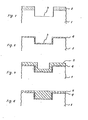
- Referring to Figs. 1 to 4, the basic process according to this invention is explained hereinafter. In the first step, a
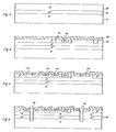
silicon substrate 1 is prepared and aphotoresist layer 2 having a predetermined pattern for forming a groove is formed thereon by a conventional photolithography technique. Thegroove 3 is formed by, for example, a conventional reactive sputter etching technique, with thephotoresist layer 2 used as an etching mask as shown in Fig. 1. The dimension of the groove depends on the type of the device to be manufactured as in the case of the conventional isolation structure. After the removal of the photoresist, the substrate is subject to a thermal oxidation treatment to form asilicon dioxide film 4 having a thickness of 500 to 1000 angstrom on the surface of thesubstrate 1 as shown in Fig. 2. Thisoxide film 4 in thegroove 3 functions as a blocking film to prevent any undesirable thermal damage or impurity diffusion in the later process steps. Thereafter, for example, aPSG layer 5 is formed on the substrate by a conventional CVD technique. The thickness of thislayer 5 should be less than the depth of thegroove 3 and also less than half of its width as shown in Fig. 3 so that thelayer 5 does not completely fill up the groove at this stage. Unnecessary portions oflayer 5 may be selectively removed so as to remain only in thegroove 3 and at its fringe. Next, a laser beam such as a carbon dioxide laser beam having a wavelength of 10.6 microns is irradiated from above onto thePSG layer 5 to melt and fluidify thePSG layer 5. The optimum condition of the irradiation energy depends on the thickness of thelayer 5. However, this condition is not critical because the laper beam is not substantially absorbed in the substrate but in thePSG layer 5 to selectively heat the same. Moreover, thePSG layer 5 tends to preferentially melt at the thick portion that is in thegroove 3 where the fluidifying of thelayer 5 is necessary because the absorption of the beam is large at this portion. Thus thePSG layer 5 is fluidified and flows into thegroove 3 due to its surface tension and its surface becomes smooth and flat as shown in Fig. 4. In this melting step, the thermally grownoxide film 4 prevents the diffusion of phosphorus which is an n type impurity into thesubstrate 1 from thePSG layer 5. In addition, any substantial thermal damage to the substrate or active elements therein by the molten PSG layer is prevented by this blockingfilm 4. - A preferred embodiment of the present invention for manufacturing a bipolar type integrated circuit device is hereinafter described with reference to Fig. 5 to Fig. 12. First of all, in a P type silicon substrate 11 having a specific resistivity of 0.1 to 0.01 ohm-cm, an
N type layer 12 having an impurity concentration of 5 x 10¹⁹ ~ 1 x 1020 cm-3 is formed by a conventional process for diffusing antimony. Thislayer 12 becomes a so-called buried diffusion layer. In contrast to a conventional process, this burieddiffusion layer 12 may be formed continuously on the entire surface of the substrate 11. Thereafter, an N typesilicon epitaxial layer 13 containing phosphorus as the N type impurity in the concentration of 5 x 1014 cm-3 is formed on the substrate by an ordinary epitaxial growth process. The resultant cross section of the substrate is shown in Fig. 1. - In the process of this embodiment, process steps for forming regions for active elements in the substrate are carried out prior to the formation of the isolation region. However, these steps are essentially the same as those in the conventional process. Referring to Fig. 6, a
silicon dioxide film 14 is formed on the substrate, Ptype base regions 15 andbase contact regions 16 of high impurity concentration are formed successively in theepitaxial layer 13 by conventional impurity diffusion processes with theoxide film 14 used as a diffusion mask. Next,emitter regions 17 andcollector regions 18 are formed by diffusion of an N type impurity in high concentration as shown in Fig. 7. Thus, the formation of active regions in the substrate for forming active elements are completed. - After the process steps described above, isolation regions are formed in the substrate as explained below. For the first step, a
groove 19 is formed in the substrate at a portion where the isolation region is to be formed as shown in Fig. 8 by a conventional reactive sputter etching technique with a photoresist film used as a mask. Thegroove 19 should be deep enough to penetrate the burieddiffusion layer 12 so as to completely isolate island-shaped N type collector regions from one another. Then, the substrate is subjected to a thermal oxidation treatment to form asilicon dioxide film 20 having a thickness of 500 to 1000 angstrom on the exposed silicon surface in thegroove 19 as shown in Fig. 9. In Fig. 10, aPSG layer 21 is formed on the substrate by a conventional CVD method. ThisPSG layer 21 should have a thickness less than the depth of thegroove 19 and also less than half of the width of thegroove 19. Typically, thegroove 19 in a bipolar type device as in this embodiment is relatively deep, for example as deep as 5 to 10 microns. On the other hand, it may be made sufficiently narrow to save area. Assuming that the width of thegroove 19 is 4 microns, the appropriate thickness of thePSG layer 21 is about 1.5 microns. - Then a laser beam generated by a carbon dioxide pulse laser is irradiated onto the
PSG layer 21 from above to melt or fluidify thelayer 21. For example, the irradiation energy is 4 to 5 joule/cm2 with the pulse width of 5 micro sec. and the diameter of the laser spot of 1 mm. The beam is preferably scanned with a pitch of 0.5 mm so that adjacent spots partially overlap one another. ThePSG layer 21 is melted instantaneously by the irradiation of the laser beam and immediately flows into thegroove 19 due to the surface tension. In this step, the blockingoxide film 20 prevents any substantial diffusion of phosphorus from the PSG layer into the substrate because the heating by the beam lasts only a very short period of time. As a result of this melting step, a smooth and flat surface as shown in Fig. 11 is obtained on the substrate. Thus the formation of the - isolation region is completed. - The succeeding process steps are the same as those in the conventional process, in which electrode windows are formed in the insulator layers on the substrate, a polycrystal silicon layer of about 400 angstrom and an aluminium layer of 5,000 to 10,000 angstrom are successively formed thereon, and patterning of the silicon and aluminium layers is carried out to form electrodes or wirings for the integrated circuit. The resultant structure is shown in Fig. 12 in which 22 is the silicon layer and 23 is the aluminium'layer. The wiring comprised of the both layers, though not shown in the Figure, extends over the
groove 19 on thePSG layer 21 without a potential risk of disconnection due to steep steps which would otherwise exist on the isolation region, i.e. on thegroove 19. - With reference to Fig. 13 to Fig. 19, a preferred embodiment of this invention for manufacturing an MIS type integrated circuit device is described hereinunder. For the first step, a
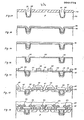
groove 32 having a depth of, for example, 1 to 2 microns is formed in a Ptype silicon substrate 31 at a portion where an field isolation region is to be formed with aphotoresist film 33 used as an etching mask. The substrate has a crystallographic surface orientation of (100) on its major surface and the abovementioned etching may be carried out by a well known unisotropic etching method so that (111) surface is exposed and the width of thegroove 32 relative to its depth can be made small. However, other etching techniques may be employed as well for the formation of thegroove 32. Thephotoresist film 33 is also used as a mask thereafter in the ion implantation process for forming a channel stop or channel cutregion 34 in thesubstrate 31 at the portion under thegroove 32. By the implantation of boron ions, the channel cutregion 34 is formed as shown in Fig. 13. - After removing the photoresist film, the substrate is subjected to a thermal oxidation treatment to form a
silicon dioxide film 35 having a thickness of 500 to 1,000 angstrom on the entire surface of the substrate. Then, apolycrystal silicon layer 36 is formed on the substrate as shown in Fig. 14. Thesilicon layer 36 has a thickness of, for example, 0.5 to 1 micron which is preferably less than half of the width of thegroove 32 as in the case of the preceeding embodiment. - Onto the silicon layer, a laser beam from a CW argon laser is irradiated to selectively heat and melt the same. An example of the optimum irradiation condition is as follows: the output power of the argon laser is 10 to 15 W, the diameter of the beam spot 50 microns, the scanning speed 10 cm/sec, the scanning pitch 25 microns. In this irradiation step, the
oxide film 35thermally insulatesthe substrate 31 from the molten silicon layer thereon so that ho part of the substrate is melted. The molten silicon flows into the groove due to surface tension so as to make its surface smooth and flat as shown in Fig. 15. - Then the
silicon layer 36 is etched until theunderlying oxide film 35 is exposed except in the groove as shown in Fig. 16. The exposed oxide film is also etched off and then the substrate is subjected to a thermal oxidation treatment to form again asilicon dioxide film 37 for a gate oxide film. The surface of the remainingsilicon layer 36 in the groove is also oxidized so that thesilicon layer 36 is completely surrounded by theoxide films oxide film 37 may be executed at this stage to adjust threshold voltage of MIS transistors to be manufactured. Another polycrystal silicon layer for forminggate electrodes 38 is formed by an ordinary CVD technique on theoxide film 37 and its patterning is carried out by a conventional photo-etching technique to formgate electrodes 38 as shown in Fig. 17. Then, phosphorus ions are implanted through theoxide film 37 to formphosphorus containing regions 39 for source or drain regions with thepolycrystal silicon layer 38 for gate used as a mask for blocking the ions. The implanted ions into thesilicon layer 38 is useful to render thelayer 38 more conductive. - A
PSG layer 40 is formed on the substrate andcontact windows 41 for source and drain are formed through thePSG layer 40 and theoxide film 37 as shown in Fig. 18. The substrate is then subjected to an annealing treatment to activate the implanted phosphorus ions to form N type source and drainregions 42. Thereafter,aluminium electrodes 43 are formed and coverPSG layer 44 is formed thereon as in the conventional device. Thus, the integrated circuit device including MIS type transistors each isolated by the field isolation structure is completed as shown in Fig. 19. - An embodiment of the present invention provides a method for forming a field isolation structure for a semiconductor device, particularly for an integrated circuit device, in which a groove is formed in a semiconductor substrate, an insulating layer is formed on the substrate at least in the groove, a glass layer or a silicon layer is formed thereon, and thereafter a high energy beam such as a laser beam is irradiated onto the glass or silicon layer to selectively heat .. the same thereby to melt or fluidify the layer and let the same flow into the groove. A smooth and flat surface is obtained through the above melting process, being effective for preventing any disconnection of wiring layers formed thereon. The method is particularly useful to obtain a minute field isolation structure effective to improve the integration density of the device.
Claims (10)
Applications Claiming Priority (2)
| Application Number | Priority Date | Filing Date | Title |
|---|---|---|---|
| JP6357380A JPS56160050A (en) | 1980-05-14 | 1980-05-14 | Semiconductor device and manufacture thereof |
| JP63573/80 | 1980-05-14 |
Publications (4)
| Publication Number | Publication Date |
|---|---|
| EP0041776A2 true EP0041776A2 (en) | 1981-12-16 |
| EP0041776A3 EP0041776A3 (en) | 1983-12-21 |
| EP0041776B1 EP0041776B1 (en) | 1986-04-16 |
| EP0041776B2 EP0041776B2 (en) | 1990-03-14 |
Family
ID=13233122
Family Applications (1)
| Application Number | Title | Priority Date | Filing Date |
|---|---|---|---|
| EP81302078A Expired - Lifetime EP0041776B2 (en) | 1980-05-14 | 1981-05-11 | Method of manufacturing a semiconductor device comprising an isolation structure |
Country Status (5)
| Country | Link |
|---|---|
| US (1) | US4404735A (en) |
| EP (1) | EP0041776B2 (en) |
| JP (1) | JPS56160050A (en) |
| DE (1) | DE3174383D1 (en) |
| IE (1) | IE51992B1 (en) |
Cited By (9)
| Publication number | Priority date | Publication date | Assignee | Title |
|---|---|---|---|---|
| EP0071010A2 (en) * | 1981-07-27 | 1983-02-09 | International Business Machines Corporation | Method for planarizing an integrated circuit structure |
| EP0071204A2 (en) * | 1981-07-27 | 1983-02-09 | International Business Machines Corporation | Method for forming recessed dielectric isolation |
| EP0071205A2 (en) * | 1981-07-27 | 1983-02-09 | International Business Machines Corporation | Method for forming high density dielectric isolation |
| EP0084265A2 (en) * | 1981-12-28 | 1983-07-27 | Fujitsu Limited | Method of producing a semiconductor device comprising a plurality of recrystallized monocrystal regions |
| EP0116789A1 (en) * | 1982-12-27 | 1984-08-29 | Fujitsu Limited | Method of producing a semiconductor device having isolation regions between elements |
| WO1986002777A1 (en) * | 1984-11-01 | 1986-05-09 | Ncr Corporation | Process for forming isolation regions in a semiconductor substrate |
| EP0208463A1 (en) * | 1985-06-24 | 1987-01-14 | GOVERNMENT OF THE UNITED STATES OF AMERICA as represented by the US department of energy | Planarization of metal films for multilevel interconnects |
| US5366905A (en) * | 1991-11-05 | 1994-11-22 | Fujitsu Limited | Method for producing conducting layers for a semiconductor device |
| EP0724291A2 (en) * | 1995-01-24 | 1996-07-31 | Nec Corporation | Semiconductor device having an improved trench isolation and method for forming the same |
Families Citing this family (26)
| Publication number | Priority date | Publication date | Assignee | Title |
|---|---|---|---|---|
| DE3279874D1 (en) * | 1981-08-21 | 1989-09-14 | Toshiba Kk | Method of manufacturing dielectric isolation regions for a semiconductor device |
| FR2513016A1 (en) * | 1981-09-14 | 1983-03-18 | Radiotechnique Compelec | HIGH VOLTAGE TRANSFORMER V MOS AND METHOD FOR MANUFACTURING THE SAME |
| JPS58210634A (en) * | 1982-05-31 | 1983-12-07 | Toshiba Corp | Preparation of semiconductor device |
| JPS59106133A (en) * | 1982-12-09 | 1984-06-19 | Nec Corp | Integrated circuit device |
| US4494303A (en) * | 1983-03-31 | 1985-01-22 | At&T Bell Laboratories | Method of making dielectrically isolated silicon devices |
| JPS6042855A (en) * | 1983-08-19 | 1985-03-07 | Hitachi Ltd | Semiconductor device |
| JPH073858B2 (en) * | 1984-04-11 | 1995-01-18 | 株式会社日立製作所 | Method for manufacturing semiconductor device |
| JPS618945A (en) * | 1984-06-25 | 1986-01-16 | Nec Corp | Semiconductor integrated circuit device |
| US4583282A (en) * | 1984-09-14 | 1986-04-22 | Motorola, Inc. | Process for self-aligned buried layer, field guard, and isolation |
| US4574469A (en) * | 1984-09-14 | 1986-03-11 | Motorola, Inc. | Process for self-aligned buried layer, channel-stop, and isolation |
| US4656497A (en) * | 1984-11-01 | 1987-04-07 | Ncr Corporation | Trench isolation structures |
| US4665010A (en) * | 1985-04-29 | 1987-05-12 | International Business Machines Corporation | Method of fabricating photopolymer isolation trenches in the surface of a semiconductor wafer |
| US4665007A (en) * | 1985-08-19 | 1987-05-12 | International Business Machines Corporation | Planarization process for organic filling of deep trenches |
| JP2584754B2 (en) * | 1986-12-01 | 1997-02-26 | キヤノン株式会社 | Communication device |
| JPH0834242B2 (en) * | 1988-12-08 | 1996-03-29 | 日本電気株式会社 | Semiconductor device and manufacturing method thereof |
| EP0459763B1 (en) | 1990-05-29 | 1997-05-02 | Semiconductor Energy Laboratory Co., Ltd. | Thin-film transistors |
| US5646450A (en) * | 1994-06-01 | 1997-07-08 | Raytheon Company | Semiconductor structures and method of manufacturing |
| US5773309A (en) * | 1994-10-14 | 1998-06-30 | The Regents Of The University Of California | Method for producing silicon thin-film transistors with enhanced forward current drive |
| US6114741A (en) * | 1996-12-13 | 2000-09-05 | Texas Instruments Incorporated | Trench isolation of a CMOS structure |
| EP0849787A1 (en) * | 1996-12-18 | 1998-06-24 | Siemens Aktiengesellschaft | Method for fabricating an integrated circuit |
| US6535535B1 (en) * | 1999-02-12 | 2003-03-18 | Semiconductor Energy Laboratory Co., Ltd. | Laser irradiation method, laser irradiation apparatus, and semiconductor device |
| US7374974B1 (en) * | 2001-03-22 | 2008-05-20 | T-Ram Semiconductor, Inc. | Thyristor-based device with trench dielectric material |
| JP3559971B2 (en) * | 2001-12-11 | 2004-09-02 | 日産自動車株式会社 | Silicon carbide semiconductor device and method of manufacturing the same |
| US7615393B1 (en) | 2008-10-29 | 2009-11-10 | Innovalight, Inc. | Methods of forming multi-doped junctions on a substrate |
| CN104170095B (en) * | 2012-03-14 | 2016-10-19 | Imec非营利协会 | For the method manufacturing the photovoltaic cell with plating contact |
| JP2014130922A (en) * | 2012-12-28 | 2014-07-10 | Toshiba Corp | Semiconductor device and manufacturing method of the same |
Citations (4)
| Publication number | Priority date | Publication date | Assignee | Title |
|---|---|---|---|---|
| DE2408402A1 (en) * | 1973-02-21 | 1974-08-22 | Raytheon Co | METHOD FOR PRODUCING INTEGRATED CIRCUITS OR INTEGRATED SEMI-CONDUCTIVE CIRCUIT UNIT MANUFACTURED BY SUCH A PROCESS |
| US3998673A (en) * | 1974-08-16 | 1976-12-21 | Pel Chow | Method for forming electrically-isolated regions in integrated circuits utilizing selective epitaxial growth |
| GB2023926A (en) * | 1978-06-22 | 1980-01-03 | Western Electric Co | Conductors for semiconductor devices |
| GB2075749A (en) * | 1980-04-28 | 1981-11-18 | Fairchild Camera Instr Co | Laser induced flow of sio-based layers in semi-conductor devices |
Family Cites Families (9)
| Publication number | Priority date | Publication date | Assignee | Title |
|---|---|---|---|---|
| JPS50118672A (en) * | 1974-03-01 | 1975-09-17 | ||
| JPS51146192A (en) * | 1975-06-11 | 1976-12-15 | Fujitsu Ltd | Diode device fabrication method |
| JPS5255877A (en) * | 1975-11-01 | 1977-05-07 | Fujitsu Ltd | Semiconductor device |
| JPS5422168A (en) * | 1977-07-20 | 1979-02-19 | Toshiba Corp | Glass coating method for semiconductor element |
| JPS54147789A (en) * | 1978-05-11 | 1979-11-19 | Matsushita Electric Ind Co Ltd | Semiconductor divice and its manufacture |
| JPS5534442A (en) * | 1978-08-31 | 1980-03-11 | Fujitsu Ltd | Preparation of semiconductor device |
| JPS5572052A (en) * | 1978-11-27 | 1980-05-30 | Fujitsu Ltd | Preparation of semiconductor device |
| US4269636A (en) * | 1978-12-29 | 1981-05-26 | Harris Corporation | Method of fabricating self-aligned bipolar transistor process and device utilizing etching and self-aligned masking |
| US4284659A (en) * | 1980-05-12 | 1981-08-18 | Bell Telephone Laboratories | Insulation layer reflow |
-
1980
- 1980-05-14 JP JP6357380A patent/JPS56160050A/en active Granted
-
1981
- 1981-05-11 DE DE8181302078T patent/DE3174383D1/en not_active Expired
- 1981-05-11 EP EP81302078A patent/EP0041776B2/en not_active Expired - Lifetime
- 1981-05-11 IE IE1040/81A patent/IE51992B1/en not_active IP Right Cessation
- 1981-05-13 US US06/263,280 patent/US4404735A/en not_active Expired - Fee Related
Patent Citations (4)
| Publication number | Priority date | Publication date | Assignee | Title |
|---|---|---|---|---|
| DE2408402A1 (en) * | 1973-02-21 | 1974-08-22 | Raytheon Co | METHOD FOR PRODUCING INTEGRATED CIRCUITS OR INTEGRATED SEMI-CONDUCTIVE CIRCUIT UNIT MANUFACTURED BY SUCH A PROCESS |
| US3998673A (en) * | 1974-08-16 | 1976-12-21 | Pel Chow | Method for forming electrically-isolated regions in integrated circuits utilizing selective epitaxial growth |
| GB2023926A (en) * | 1978-06-22 | 1980-01-03 | Western Electric Co | Conductors for semiconductor devices |
| GB2075749A (en) * | 1980-04-28 | 1981-11-18 | Fairchild Camera Instr Co | Laser induced flow of sio-based layers in semi-conductor devices |
Cited By (16)
| Publication number | Priority date | Publication date | Assignee | Title |
|---|---|---|---|---|
| EP0071205A3 (en) * | 1981-07-27 | 1986-08-20 | International Business Machines Corporation | Method for forming high density dielectric isolation |
| EP0071204A2 (en) * | 1981-07-27 | 1983-02-09 | International Business Machines Corporation | Method for forming recessed dielectric isolation |
| EP0071205A2 (en) * | 1981-07-27 | 1983-02-09 | International Business Machines Corporation | Method for forming high density dielectric isolation |
| EP0071010A2 (en) * | 1981-07-27 | 1983-02-09 | International Business Machines Corporation | Method for planarizing an integrated circuit structure |
| EP0071010A3 (en) * | 1981-07-27 | 1984-11-28 | International Business Machines Corporation | Method for planarizing an integrated circuit structure |
| EP0071204A3 (en) * | 1981-07-27 | 1986-08-20 | International Business Machines Corporation | Method for forming recessed dielectric isolation |
| EP0084265A2 (en) * | 1981-12-28 | 1983-07-27 | Fujitsu Limited | Method of producing a semiconductor device comprising a plurality of recrystallized monocrystal regions |
| EP0084265A3 (en) * | 1981-12-28 | 1985-04-17 | Fujitsu Limited | Method of producing a semiconductor device comprising a plurality of recrystallized monocrystal regions |
| EP0116789A1 (en) * | 1982-12-27 | 1984-08-29 | Fujitsu Limited | Method of producing a semiconductor device having isolation regions between elements |
| US4611386A (en) * | 1982-12-27 | 1986-09-16 | Fujitsu Limited | Method of producing a semiconductor device |
| WO1986002777A1 (en) * | 1984-11-01 | 1986-05-09 | Ncr Corporation | Process for forming isolation regions in a semiconductor substrate |
| EP0208463A1 (en) * | 1985-06-24 | 1987-01-14 | GOVERNMENT OF THE UNITED STATES OF AMERICA as represented by the US department of energy | Planarization of metal films for multilevel interconnects |
| US5366905A (en) * | 1991-11-05 | 1994-11-22 | Fujitsu Limited | Method for producing conducting layers for a semiconductor device |
| EP0724291A2 (en) * | 1995-01-24 | 1996-07-31 | Nec Corporation | Semiconductor device having an improved trench isolation and method for forming the same |
| EP0724291A3 (en) * | 1995-01-24 | 1998-03-11 | Nec Corporation | Semiconductor device having an improved trench isolation and method for forming the same |
| US5966598A (en) * | 1995-01-24 | 1999-10-12 | Nec Corporation | Semiconductor device having an improved trench isolation and method for forming the same |
Also Published As
| Publication number | Publication date |
|---|---|
| IE51992B1 (en) | 1987-05-13 |
| EP0041776A3 (en) | 1983-12-21 |
| IE811040L (en) | 1981-11-14 |
| US4404735A (en) | 1983-09-20 |
| JPH0210575B2 (en) | 1990-03-08 |
| DE3174383D1 (en) | 1986-05-22 |
| EP0041776B2 (en) | 1990-03-14 |
| EP0041776B1 (en) | 1986-04-16 |
| JPS56160050A (en) | 1981-12-09 |
Similar Documents
| Publication | Publication Date | Title |
|---|---|---|
| EP0041776B1 (en) | Method of manufacturing a semiconductor device comprising an isolation structure | |
| KR900000561B1 (en) | Manufacturing method of an ic and device | |
| US4415383A (en) | Method of fabricating semiconductor devices using laser annealing | |
| EP0037261B1 (en) | A method of manufacturing a semiconductor device, and a device, for example a bomis fet, so manufactured | |
| EP0072216B1 (en) | The production of semiconductor devices by methods involving annealing | |
| US4381201A (en) | Method for production of semiconductor devices | |
| JP4295922B2 (en) | Gas immersion laser annealing method suitable for application in the fabrication of small integrated circuits | |
| US3913211A (en) | Method of MOS transistor manufacture | |
| EP0015677B1 (en) | Method of producing semiconductor devices | |
| US5405804A (en) | Method of manufacturing a semiconductor device by laser annealing a metal layer through an insulator | |
| US4267011A (en) | Method for manufacturing a semiconductor device | |
| US4407060A (en) | Method of manufacturing a semiconductor device | |
| CA1237828A (en) | Semiconductor-on-insulator (soi) device having electrical short to avoid charge accumulation | |
| EP0038178A1 (en) | Method of manufacturing a semiconductor device containing a Schottky barrier, and device | |
| US5284794A (en) | Method of making semiconductor device using a trimmable thin-film resistor | |
| EP0045593A2 (en) | Process for producing semiconductor device | |
| US4137100A (en) | Forming isolation and device regions due to enhanced diffusion of impurities in semiconductor material by laser | |
| US4835113A (en) | Fabrication of dielectrically isolated devices with buried conductive layers | |
| US3895392A (en) | Bipolar transistor structure having ion implanted region and method | |
| US4649626A (en) | Semiconductor on insulator edge doping process using an expanded mask | |
| EP0084985A2 (en) | Laser induced flow Ge-O based materials | |
| RU1830156C (en) | Method of producing semiconducting device | |
| EP0076147A2 (en) | Method of producing a semiconductor device comprising an isolation region | |
| JPH0677155A (en) | Heat treatment method for semiconductor substrate | |
| CA1161969A (en) | Method of fabricating semiconductor devices using laser annealing |
Legal Events
| Date | Code | Title | Description |
|---|---|---|---|
| PUAI | Public reference made under article 153(3) epc to a published international application that has entered the european phase |
Free format text: ORIGINAL CODE: 0009012 |
|
| AK | Designated contracting states |
Designated state(s): DE FR GB NL |
|
| RBV | Designated contracting states (corrected) |
Designated state(s): DE FR GB NL |
|
| PUAL | Search report despatched |
Free format text: ORIGINAL CODE: 0009013 |
|
| AK | Designated contracting states |
Designated state(s): DE FR GB NL |
|
| 17P | Request for examination filed |
Effective date: 19840105 |
|
| GRAA | (expected) grant |
Free format text: ORIGINAL CODE: 0009210 |
|
| AK | Designated contracting states |
Kind code of ref document: B1 Designated state(s): DE FR GB NL |
|
| ET | Fr: translation filed | ||
| REF | Corresponds to: |
Ref document number: 3174383 Country of ref document: DE Date of ref document: 19860522 |
|
| PLBI | Opposition filed |
Free format text: ORIGINAL CODE: 0009260 |
|
| 26 | Opposition filed |
Opponent name: SIEMENS AKTIENGESELLSCHAFT, BERLIN UND MUENCHEN Effective date: 19870115 |
|
| NLR1 | Nl: opposition has been filed with the epo |
Opponent name: SIEMENS AKTIENGESELLSCHAFT |
|
| PUAH | Patent maintained in amended form |
Free format text: ORIGINAL CODE: 0009272 |
|
| STAA | Information on the status of an ep patent application or granted ep patent |
Free format text: STATUS: PATENT MAINTAINED AS AMENDED |
|
| 27A | Patent maintained in amended form |
Effective date: 19900314 |
|
| AK | Designated contracting states |
Kind code of ref document: B2 Designated state(s): DE FR GB NL |
|
| ET3 | Fr: translation filed ** decision concerning opposition | ||
| NLR2 | Nl: decision of opposition | ||
| NLR3 | Nl: receipt of modified translations in the netherlands language after an opposition procedure | ||
| PGFP | Annual fee paid to national office [announced via postgrant information from national office to epo] |
Ref country code: GB Payment date: 19930309 Year of fee payment: 13 |
|
| PGFP | Annual fee paid to national office [announced via postgrant information from national office to epo] |
Ref country code: FR Payment date: 19930526 Year of fee payment: 13 |
|
| PGFP | Annual fee paid to national office [announced via postgrant information from national office to epo] |
Ref country code: NL Payment date: 19930531 Year of fee payment: 13 |
|
| PGFP | Annual fee paid to national office [announced via postgrant information from national office to epo] |
Ref country code: DE Payment date: 19930724 Year of fee payment: 13 |
|
| PG25 | Lapsed in a contracting state [announced via postgrant information from national office to epo] |
Ref country code: GB Effective date: 19940511 |
|
| PG25 | Lapsed in a contracting state [announced via postgrant information from national office to epo] |
Ref country code: NL Effective date: 19941201 |
|
| GBPC | Gb: european patent ceased through non-payment of renewal fee |
Effective date: 19940511 |
|
| NLV4 | Nl: lapsed or anulled due to non-payment of the annual fee | ||
| PG25 | Lapsed in a contracting state [announced via postgrant information from national office to epo] |
Ref country code: FR Effective date: 19950131 |
|
| PG25 | Lapsed in a contracting state [announced via postgrant information from national office to epo] |
Ref country code: DE Effective date: 19950201 |
|
| REG | Reference to a national code |
Ref country code: FR Ref legal event code: ST |
|
| APAC | Appeal dossier modified |
Free format text: ORIGINAL CODE: EPIDOS NOAPO |
|
| APAC | Appeal dossier modified |
Free format text: ORIGINAL CODE: EPIDOS NOAPO |
|
| APAH | Appeal reference modified |
Free format text: ORIGINAL CODE: EPIDOSCREFNO |