EP0031260B1 - Procédé d'alignement de photogravures par rapport aux murs d'isolement de caisson dans des circuits intégrés - Google Patents
Procédé d'alignement de photogravures par rapport aux murs d'isolement de caisson dans des circuits intégrés Download PDFInfo
- Publication number
- EP0031260B1 EP0031260B1 EP80401616A EP80401616A EP0031260B1 EP 0031260 B1 EP0031260 B1 EP 0031260B1 EP 80401616 A EP80401616 A EP 80401616A EP 80401616 A EP80401616 A EP 80401616A EP 0031260 B1 EP0031260 B1 EP 0031260B1
- Authority
- EP
- European Patent Office
- Prior art keywords
- substrate
- isolation walls
- caissons
- layer
- conductivity type
- Prior art date
- Legal status (The legal status is an assumption and is not a legal conclusion. Google has not performed a legal analysis and makes no representation as to the accuracy of the status listed.)
- Expired
Links
Images
Classifications
-
- H10P90/191—
-
- H10P50/00—
-
- H10W10/031—
-
- H10W10/181—
-
- H10W10/30—
-
- Y—GENERAL TAGGING OF NEW TECHNOLOGICAL DEVELOPMENTS; GENERAL TAGGING OF CROSS-SECTIONAL TECHNOLOGIES SPANNING OVER SEVERAL SECTIONS OF THE IPC; TECHNICAL SUBJECTS COVERED BY FORMER USPC CROSS-REFERENCE ART COLLECTIONS [XRACs] AND DIGESTS
- Y10—TECHNICAL SUBJECTS COVERED BY FORMER USPC
- Y10S—TECHNICAL SUBJECTS COVERED BY FORMER USPC CROSS-REFERENCE ART COLLECTIONS [XRACs] AND DIGESTS
- Y10S148/00—Metal treatment
- Y10S148/085—Isolated-integrated
-
- Y—GENERAL TAGGING OF NEW TECHNOLOGICAL DEVELOPMENTS; GENERAL TAGGING OF CROSS-SECTIONAL TECHNOLOGIES SPANNING OVER SEVERAL SECTIONS OF THE IPC; TECHNICAL SUBJECTS COVERED BY FORMER USPC CROSS-REFERENCE ART COLLECTIONS [XRACs] AND DIGESTS
- Y10—TECHNICAL SUBJECTS COVERED BY FORMER USPC
- Y10S—TECHNICAL SUBJECTS COVERED BY FORMER USPC CROSS-REFERENCE ART COLLECTIONS [XRACs] AND DIGESTS
- Y10S148/00—Metal treatment
- Y10S148/117—Oxidation, selective
-
- Y—GENERAL TAGGING OF NEW TECHNOLOGICAL DEVELOPMENTS; GENERAL TAGGING OF CROSS-SECTIONAL TECHNOLOGIES SPANNING OVER SEVERAL SECTIONS OF THE IPC; TECHNICAL SUBJECTS COVERED BY FORMER USPC CROSS-REFERENCE ART COLLECTIONS [XRACs] AND DIGESTS
- Y10—TECHNICAL SUBJECTS COVERED BY FORMER USPC
- Y10S—TECHNICAL SUBJECTS COVERED BY FORMER USPC CROSS-REFERENCE ART COLLECTIONS [XRACs] AND DIGESTS
- Y10S148/00—Metal treatment
- Y10S148/151—Simultaneous diffusion
Definitions
- the present invention relates to a method of aligning photoengravings with respect to the isolation walls of boxes in integrated circuits and integrated structures incorporating such boxes. It applies more particularly to bipolar integrated circuits in which the thickness of the epitaxial layer is of the order of only a few microns.
- each elementary component of the integrated circuit is formed inside a box intended to ensure the operation of this component independently of the phenomena which can occur in the zones corresponding to the neighboring components.
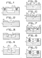
- FIG. 1 represents a bipolar integrated circuit box obtained in a conventional manner.
- This box is formed on a semiconductor substrate, commonly silicon designated by the reference 1. It is delimited laterally by a zone 2 of type P + having a closed contour, commonly of square or rectangular shape. Between the lower part of the box and the substrate 1 is often formed a buried layer 3 of the same type of conductivity as the box, and of the type of conductivity opposite to that of the substrate, for example of type N + if the substrate is of type P and the N type box.
- this box of type N, is formed by initially implanting in the substrate P, substantially at the locations of the layer intended to become the buried layer 3, doping impurities at high concentration, then by growing an epitaxial layer 4 on the substrate and finally by diffusing through an appropriate mask to form the isolation walls 2 of the box.
- One of the known methods consists, as shown in FIG. 2, of etching in an oxide layer 10 formed on the surface of the substrate 1 of the openings 11 in which the buried layers 12 of the N + type will be implanted.
- heat treatment is carried out at elevated temperature in a slightly oxidizing atmosphere.
- the growth of the faster silica layer at the level of the apparent silicon of the buried layer causes a depression in the surface of the silicon above this buried layer.
- This unevenness shows a step 13 which delimits the periphery of the buried layer.
- the orientation of this step being different from the rest of the surface of the substrate and the epitaxial growth being anisotropic, the growth of the silicon will take place obliquely with respect to the step.
- Another prior art method for positioning the isolation mask with respect to the buried layer consists in taking a mark on the rear face of the substrate. This mark produced during the etching of the buried layer requires an optical polished rear face to that its geometrical definition is sufficient during alignment. But with the methods used, the precision is even less good than previously and is all the worse when the plate is thick, which limits its use to small diameter plates or to power devices whose alignment is not very critical.
- an object of the present invention is to alleviate the above-mentioned drawbacks of the prior art and to provide a box-forming method allowing extremely precise alignment of the isolation walls with respect to the buried layer of a integrated circuit.
- the present invention provides a method of aligning the photo-engravings carried out in each box with respect to the isolation walls of boxes in integrated circuits, these boxes being formed.
- this method consisting in implanting doping impurities (26) of the second type of conductivity in the substrate along the contour of the isolation walls, then, after formation of the epitaxial layer, in diffusing these impurities towards and up to the surface of the epitaxial layer, further comprising the step of making the surface outcrop area of the isolation walls visible.
- One embodiment consists in anodizing the wafers to transform the isolation walls into doped monocrystalline silicon of the same type of conductivity as the substrate in porous silicon, then in carrying out an oxidizing treatment to transform the porous silicon into silica (Fig. 11 ).
- Another embodiment consists in subjecting the surface of the wafer to a chemical attack, selective according to the type of conductivity (FIG. 10).
- openings 21 are engraved in the silica layer 10, in one operation, instead of one.
- the openings 21 will be diffused the buried layers N + and in the openings 22 the foundations of the isolation walls will be formed later.
- the photographic mask used includes the patterns corresponding to the buried layers and the isolation walls.
- the relative position of the two regions is therefore defined by the photographic definition of the mask; it is currently around 0.1 ⁇ .
- a layer 23 of a photo-sensitive lacquer or resin is spread over the silica layer 10 and its openings 21 and 22, this layer is then impressed through a mask comprising only the patterns of the buried layer. These patterns are slightly enlarged, by 2 ⁇ for example, so as to allow their alignment with respect to the previously engraved patterns.
- the resin then developed, releases the openings 21 while obstructing the openings 22.
- the implantation of the dopant is then carried out to form the buried layer 12.
- the implantation of a dose of arsenic of 5 ⁇ 10 15 at / cm 2 with an energy of 100 keV allows, after diffusion, to obtain layer resistances of 10 necessary for this kind of item.
- the diffusion providing the buried layer 3 is carried out so as to restore the defects caused by the implantation and to form a thin oxide layer 24, a layer which prevents the loss of arsenic (see FIG. 7).
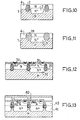
- Figure 7 shows the wafer in the next step, a layer of photosensitive resin 25 covers the buried layer regions so as to limit the implantation of boron at the openings 22 of the wall foundations.
- the photographic mask used for this operation includes the patterns of the isolation walls slightly enlarged as before; an enlargement of 2 p. allows a positioning tolerance of ⁇ 1 ⁇ , but requires that on the first mask the patterns of the buried layers be more than 2 ⁇ from those of the isolation walls. This constraint however allows the isolation foundations to come into contact with the buried layer by lateral diffusion if it is necessary to reduce the dimension of the caissons as much as possible.
- foundations 26 doped with boron is then carried out, with an energy chosen so that the ions do not pass through either the resin layer or the thicker oxide layer which has grown initially.
- An oxide layer of 1 ⁇ and an energy of 200 keV allow the boron to be placed deep enough to avoid its exodiffusion during epitaxy.
- the thin oxide layer (50 nm) created during the annealing of the buried layer can be eliminated either before or after implantation depending on the dose of boron implanted, it is in any case of thickness too small to mask the implantation under the chosen conditions.
- a boron dose of 5 x lo ' S at./C M 2 @ for example, will be sufficient to obtain by diffusion a complete crossing of the epitaxial layer unless the buried layer rises in a too sensitive way.
- FIG. 8 represents the plate after the growth of the epitaxial layer and the isolation diffusions.
- the foundations 26 have given rise to P-type isolation walls 30 which delimit insulated caissons in the N-type epitaxial layer.
- the distance between the isolation walls and the buried layer can therefore be closely controlled: these walls can be arranged as shown schematically in Figure 8, or they can be strictly added to the layer buried, or alternatively, as illustrated in FIG. 9, the junctions of the isolation walls can penetrate symmetrically into the lateral diffusion of the buried layer.
- the ridge of the walls one can proceed in two ways: either by digging, by selective chemical attack according to the type of conductivity, the ridge of the isolation walls P (Fig. 10), or by transforming the silicon which constitutes them made of porous silicon by anodic attack. Both methods have been successfully tried.
- the second method is particularly useful in the case of structures such as that of FIG. 9. It is then desirable to transform the porous silicon of the walls into oxide 28 (Fig. 11) if one does not want to reduce in a way excessive the insulation voltage withstand of the box.
- the method described therefore makes it possible in particular to obtain a lateral dielectric isolation aligned with the periphery of the buried layers; this arrangement makes it possible in particular to produce devices simultaneously comprising boxes whose bottom is isolated either by the junction between the substrate and the epitaxial layer, or by that of the buried layer described above and the substrate.
- FIG. 12 represents two adjacent boxes 30 and 31 formed according to the present invention.
- the well 30 does not include a buried layer and contains a PNP transistor - conventional substrate.
- the box 31 comprises a buried layer 32 whose edges come into contact with the foundations of silica isolation walls.
- the well 31 contains a conventional NPN transistor.
- the gain of the PNP parasitic transistor thus formed depends largely on the distance between the isolation foundation and the buried layer since in this space the operation is identical to that of an authentic PNP transistor substrate. It is then obvious that all relative variations in the insulation and the buried layer will lead to significant variations in the gain of this parasitic element and therefore to malfunctions of the integrated circuit itself.
- the method described above makes it possible to exactly control this isolation distance / buried layer and therefore the gain of the parasitic transistors.
- FIG. 13 represents the caissons 40 provided with buried layers 41, adjacent to isolation walls 33 made of silicon oxide.
- the element leading to a parasitic current in the substrate can be a metal / semiconductor diode (42/43) called a Schottky diode.
- a Schottky diode This kind of arrangement is frequently encountered in programmable bipolar memories. These memories consist of a matrix of Schottky diodes, matrix in which the access to each diode is formed by a metal connection not shown and which can be melted for a high intensity.
- the exemplary embodiment which is proposed is not limiting: it could for example for boxes of very small thickness ( ⁇ 1 ⁇ ) instead of depositing the epitaxial layer at high temperature by chemical decomposition d '' a hydrogenated or chlorinated silicon compound, deposit this silicon in an amorphous form to many lower temperature, a surface annealing thanks to a laser or an electron beam leading simultaneously to an epitaxial recrystallization of the layer and to the diffusion of isolations.
Landscapes
- Element Separation (AREA)
Applications Claiming Priority (2)
| Application Number | Priority Date | Filing Date | Title |
|---|---|---|---|
| FR7931483A FR2472268A1 (fr) | 1979-12-21 | 1979-12-21 | Procede de formation de caisson dans des circuits integres |
| FR7931483 | 1979-12-21 |
Publications (3)
| Publication Number | Publication Date |
|---|---|
| EP0031260A2 EP0031260A2 (fr) | 1981-07-01 |
| EP0031260A3 EP0031260A3 (en) | 1981-07-22 |
| EP0031260B1 true EP0031260B1 (fr) | 1983-11-23 |
Family
ID=9233091
Family Applications (1)
| Application Number | Title | Priority Date | Filing Date |
|---|---|---|---|
| EP80401616A Expired EP0031260B1 (fr) | 1979-12-21 | 1980-11-12 | Procédé d'alignement de photogravures par rapport aux murs d'isolement de caisson dans des circuits intégrés |
Country Status (4)
| Country | Link |
|---|---|
| US (1) | US4369561A (OSRAM) |
| EP (1) | EP0031260B1 (OSRAM) |
| DE (1) | DE3065715D1 (OSRAM) |
| FR (1) | FR2472268A1 (OSRAM) |
Families Citing this family (3)
| Publication number | Priority date | Publication date | Assignee | Title |
|---|---|---|---|---|
| US4532700A (en) * | 1984-04-27 | 1985-08-06 | International Business Machines Corporation | Method of manufacturing semiconductor structures having an oxidized porous silicon isolation layer |
| US4627883A (en) * | 1985-04-01 | 1986-12-09 | Gte Laboratories Incorporated | Method of forming an isolated semiconductor structure |
| JPH01179342A (ja) * | 1988-01-05 | 1989-07-17 | Toshiba Corp | 複合半導体結晶体 |
Family Cites Families (7)
| Publication number | Priority date | Publication date | Assignee | Title |
|---|---|---|---|---|
| US3713908A (en) * | 1970-05-15 | 1973-01-30 | Ibm | Method of fabricating lateral transistors and complementary transistors |
| DE2044863A1 (de) * | 1970-09-10 | 1972-03-23 | Siemens Ag | Verfahren zur Herstellung von Schottkydioden |
| GB1501114A (en) * | 1974-04-25 | 1978-02-15 | Rca Corp | Method of making a semiconductor device |
| US3919060A (en) * | 1974-06-14 | 1975-11-11 | Ibm | Method of fabricating semiconductor device embodying dielectric isolation |
| US3954523A (en) * | 1975-04-14 | 1976-05-04 | International Business Machines Corporation | Process for fabricating devices having dielectric isolation utilizing anodic treatment and selective oxidation |
| GB1503223A (en) * | 1975-07-26 | 1978-03-08 | Int Computers Ltd | Formation of buried layers in a substrate |
| US4016017A (en) * | 1975-11-28 | 1977-04-05 | International Business Machines Corporation | Integrated circuit isolation structure and method for producing the isolation structure |
-
1979
- 1979-12-21 FR FR7931483A patent/FR2472268A1/fr active Granted
-
1980
- 1980-11-12 DE DE8080401616T patent/DE3065715D1/de not_active Expired
- 1980-11-12 EP EP80401616A patent/EP0031260B1/fr not_active Expired
- 1980-12-04 US US06/212,974 patent/US4369561A/en not_active Expired - Lifetime
Also Published As
| Publication number | Publication date |
|---|---|
| DE3065715D1 (en) | 1983-12-29 |
| FR2472268A1 (fr) | 1981-06-26 |
| EP0031260A3 (en) | 1981-07-22 |
| US4369561A (en) | 1983-01-25 |
| FR2472268B1 (OSRAM) | 1983-10-14 |
| EP0031260A2 (fr) | 1981-07-01 |
Similar Documents
| Publication | Publication Date | Title |
|---|---|---|
| EP0179693B1 (fr) | Structure de circuit intégré comportant des transistors CMOS à tenue en tension élevée, et son procédé de fabrication | |
| EP0038238B1 (fr) | Procédé de fabrication d'un dispositif semiconducteur à grille profonde accessible par la surface | |
| EP0462882A1 (fr) | Transistor à effet de champ en couche mince avec grille enterrée et son procédé de fabrication | |
| EP0057126B1 (fr) | Procédé de fabrication d'une structure de transistors | |
| EP0203836B1 (fr) | Procédé de fabrication de transistors à effet de champ, et transistors bipolaires latéraux sur un même substrat | |
| EP0164281A1 (fr) | Procédé de fabrication d'une couche isolante enterrée dans un substrat semiconducteur, par implantation ionique | |
| JPH0797625B2 (ja) | 半導体記憶装置 | |
| EP0004292A2 (fr) | Procédé de fabrication d'un transistor bipolaire de type MESA présentant des régions d'émetteur et de base auto-alignées | |
| US3948694A (en) | Self-aligned method for integrated circuit manufacture | |
| EP0031260B1 (fr) | Procédé d'alignement de photogravures par rapport aux murs d'isolement de caisson dans des circuits intégrés | |
| FR3067516A1 (fr) | Realisation de regions semiconductrices dans une puce electronique | |
| US5147809A (en) | Method of producing a bipolar transistor with a laterally graded emitter (LGE) employing a refill method of polycrystalline silicon | |
| FR2475293A1 (fr) | Procede de fabrication de transistor bipolaire lateral auto-aligne | |
| FR2483685A1 (fr) | Transistor de puissance a effet de champ (fet) du type v-mos a grille maillee | |
| FR3040538A1 (fr) | Transistor mos et son procede de fabrication | |
| FR2548831A1 (fr) | Procede de realisation d'au moins une couche profonde dans un dispositif a semi-conducteur | |
| US6599817B1 (en) | Semiconductor constructions, and methods of forming semiconductor constructions | |
| FR2790867A1 (fr) | Procede de fabrication de transistor bipolaire | |
| EP0401135A1 (fr) | Procédé de fabrication simultanée de transistors MOS à canal N et de transistors bipolaires verticaux PNP | |
| JP2007129033A (ja) | アバランシェフォトダイオードおよびその製造方法 | |
| EP1291922A1 (fr) | Structure de contact sur une région profonde formée dans un substrat semiconducteur | |
| EP0024222B1 (fr) | Procédé de fabrication d'un transistor à effet de champ à grille SCHOTTKY autoalignée | |
| FR2854276A1 (fr) | Dispositif semiconducteur comprenant des extensions realisees en un materiau a faible temperature de fusion. | |
| EP0230824B1 (fr) | Procédé de fabrication d'un caisson et éventuellement de zones d'isolation électriques d'un circuit intégré, notamment de type MOS | |
| EP1146554A1 (fr) | Procédé de formation de couches enterrées |
Legal Events
| Date | Code | Title | Description |
|---|---|---|---|
| PUAI | Public reference made under article 153(3) epc to a published international application that has entered the european phase |
Free format text: ORIGINAL CODE: 0009012 |
|
| PUAL | Search report despatched |
Free format text: ORIGINAL CODE: 0009013 |
|
| AK | Designated contracting states |
Designated state(s): DE FR GB IT |
|
| AK | Designated contracting states |
Designated state(s): DE FR GB IT |
|
| 17P | Request for examination filed |
Effective date: 19810807 |
|
| ITF | It: translation for a ep patent filed | ||
| RBV | Designated contracting states (corrected) |
Designated state(s): DE FR GB IT |
|
| GRAA | (expected) grant |
Free format text: ORIGINAL CODE: 0009210 |
|
| AK | Designated contracting states |
Designated state(s): DE FR GB IT |
|
| REF | Corresponds to: |
Ref document number: 3065715 Country of ref document: DE Date of ref document: 19831229 |
|
| PLBE | No opposition filed within time limit |
Free format text: ORIGINAL CODE: 0009261 |
|
| STAA | Information on the status of an ep patent application or granted ep patent |
Free format text: STATUS: NO OPPOSITION FILED WITHIN TIME LIMIT |
|
| 26N | No opposition filed | ||
| ITTA | It: last paid annual fee | ||
| PGFP | Annual fee paid to national office [announced via postgrant information from national office to epo] |
Ref country code: FR Payment date: 19991109 Year of fee payment: 20 |
|
| PGFP | Annual fee paid to national office [announced via postgrant information from national office to epo] |
Ref country code: GB Payment date: 19991110 Year of fee payment: 20 |
|
| PGFP | Annual fee paid to national office [announced via postgrant information from national office to epo] |
Ref country code: DE Payment date: 19991115 Year of fee payment: 20 |
|
| REG | Reference to a national code |
Ref country code: FR Ref legal event code: D6 |
|
| PG25 | Lapsed in a contracting state [announced via postgrant information from national office to epo] |
Ref country code: GB Free format text: LAPSE BECAUSE OF EXPIRATION OF PROTECTION Effective date: 20001111 |
|
| REG | Reference to a national code |
Ref country code: GB Ref legal event code: PE20 Effective date: 20001111 |