EP0030168B1 - Dispositif de mise en parallèle de transistors de puissance en très haute fréquence - Google Patents
Dispositif de mise en parallèle de transistors de puissance en très haute fréquence Download PDFInfo
- Publication number
- EP0030168B1 EP0030168B1 EP80401449A EP80401449A EP0030168B1 EP 0030168 B1 EP0030168 B1 EP 0030168B1 EP 80401449 A EP80401449 A EP 80401449A EP 80401449 A EP80401449 A EP 80401449A EP 0030168 B1 EP0030168 B1 EP 0030168B1
- Authority
- EP
- European Patent Office
- Prior art keywords
- transistors
- plate
- electrodes
- high frequency
- terminals
- Prior art date
- Legal status (The legal status is an assumption and is not a legal conclusion. Google has not performed a legal analysis and makes no representation as to the accuracy of the status listed.)
- Expired
Links
Images
Classifications
-
- H—ELECTRICITY
- H01—ELECTRIC ELEMENTS
- H01L—SEMICONDUCTOR DEVICES NOT COVERED BY CLASS H10
- H01L23/00—Details of semiconductor or other solid state devices
- H01L23/02—Containers; Seals
- H01L23/04—Containers; Seals characterised by the shape of the container or parts, e.g. caps, walls
- H01L23/053—Containers; Seals characterised by the shape of the container or parts, e.g. caps, walls the container being a hollow construction and having an insulating or insulated base as a mounting for the semiconductor body
- H01L23/057—Containers; Seals characterised by the shape of the container or parts, e.g. caps, walls the container being a hollow construction and having an insulating or insulated base as a mounting for the semiconductor body the leads being parallel to the base
-
- H—ELECTRICITY
- H01—ELECTRIC ELEMENTS
- H01L—SEMICONDUCTOR DEVICES NOT COVERED BY CLASS H10
- H01L23/00—Details of semiconductor or other solid state devices
- H01L23/52—Arrangements for conducting electric current within the device in operation from one component to another, i.e. interconnections, e.g. wires, lead frames
- H01L23/538—Arrangements for conducting electric current within the device in operation from one component to another, i.e. interconnections, e.g. wires, lead frames the interconnection structure between a plurality of semiconductor chips being formed on, or in, insulating substrates
-
- H—ELECTRICITY
- H01—ELECTRIC ELEMENTS
- H01L—SEMICONDUCTOR DEVICES NOT COVERED BY CLASS H10
- H01L23/00—Details of semiconductor or other solid state devices
- H01L23/58—Structural electrical arrangements for semiconductor devices not otherwise provided for, e.g. in combination with batteries
- H01L23/64—Impedance arrangements
- H01L23/66—High-frequency adaptations
-
- H—ELECTRICITY
- H01—ELECTRIC ELEMENTS
- H01L—SEMICONDUCTOR DEVICES NOT COVERED BY CLASS H10
- H01L25/00—Assemblies consisting of a plurality of semiconductor or other solid state devices
- H01L25/03—Assemblies consisting of a plurality of semiconductor or other solid state devices all the devices being of a type provided for in a single subclass of subclasses H10B, H10D, H10F, H10H, H10K or H10N, e.g. assemblies of rectifier diodes
- H01L25/04—Assemblies consisting of a plurality of semiconductor or other solid state devices all the devices being of a type provided for in a single subclass of subclasses H10B, H10D, H10F, H10H, H10K or H10N, e.g. assemblies of rectifier diodes the devices not having separate containers
- H01L25/07—Assemblies consisting of a plurality of semiconductor or other solid state devices all the devices being of a type provided for in a single subclass of subclasses H10B, H10D, H10F, H10H, H10K or H10N, e.g. assemblies of rectifier diodes the devices not having separate containers the devices being of a type provided for in group subclass H10D
- H01L25/072—Assemblies consisting of a plurality of semiconductor or other solid state devices all the devices being of a type provided for in a single subclass of subclasses H10B, H10D, H10F, H10H, H10K or H10N, e.g. assemblies of rectifier diodes the devices not having separate containers the devices being of a type provided for in group subclass H10D the devices being arranged next to each other
-
- H—ELECTRICITY
- H01—ELECTRIC ELEMENTS
- H01L—SEMICONDUCTOR DEVICES NOT COVERED BY CLASS H10
- H01L2223/00—Details relating to semiconductor or other solid state devices covered by the group H01L23/00
- H01L2223/58—Structural electrical arrangements for semiconductor devices not otherwise provided for
- H01L2223/64—Impedance arrangements
- H01L2223/66—High-frequency adaptations
- H01L2223/6644—Packaging aspects of high-frequency amplifiers
-
- H—ELECTRICITY
- H01—ELECTRIC ELEMENTS
- H01L—SEMICONDUCTOR DEVICES NOT COVERED BY CLASS H10
- H01L2924/00—Indexing scheme for arrangements or methods for connecting or disconnecting semiconductor or solid-state bodies as covered by H01L24/00
- H01L2924/0001—Technical content checked by a classifier
- H01L2924/0002—Not covered by any one of groups H01L24/00, H01L24/00 and H01L2224/00
Definitions
- the invention relates to a device for paralleling transistors, at very high frequency, in particular those intended to be placed between an input line and an output line with two parallel conducting planes.
- the invention also relates to a very high frequency and high power amplifier, for example of 500 watts, using such a device.
- the bipolar transistors are frequently mounted in the circuits of use by isolating the collector from the ground. This results in practice in the need to isolate from the ground the rear face of the substrate of the transistor (that which is opposite to the face comprising the base and emitter electrodes).
- the invention makes it possible to resolve a large part of these difficulties.
- a device for paralleling 2n transistors (n being an integer equal to or greater than one) intended to operate at high power, at very high frequency, of the type comprising a first plate serving as an electrical ground plane and thermal and a second electrically insulating plate, supporting two metallized areas, each transistor being placed on one of 2n electrically insulating and thermally conductive plates soldered to the first plate, the transistors, arranged in n columns, being inserted between the first and the second plate, is characterized in that the insulating plates supporting the different transistors are provided with at least three terminals respectively connected to each of the electrodes of the transistors, one of which is grounded and the other two support pins constituting conductors passing through the second plate and coming respectively to connect one or the other of the metallized areas.
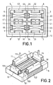
- the collector of the transistor is produced in a region of the substrate which is flush with the rear face of the latter.
- the substrate is itself welded by this face to a metallized area 51 of the wafer 5.
- This area has a surface which extends beyond the chip and extends under the terminals 13 and 14, one or the other of which can serve as collector terminal.
- the metallized area 51 is visible in FIG. 2 between the chip 1 and the terminals 13 and 14.
- the terminal used for the electrical connection with the circuit external to the transistor is for example the terminal 14 occupying, as seen in FIG. 1, a more central in the box tier than terminal 13.
- terminal 12 is connected to the bottom of the housing by means of a metallized pad 52 deposited on the edge of the wafer and projecting over the two large faces of the latter.
- the four terminals 11 to 14 of the same transistor are for example formed using golden copper bands folded in a U shape and soldered on the wafer 5.
- the terminals 11 and 14 support cylindrical pins (such as 111 for terminal 11) with axes perpendicular to the bottom of the housing. Terminals 12 and 13 do not have such pins.
- the pins of terminals 14, 24, 34 and 44 occupy a more central position than the pins of terminals 11, 21, 31 and 41.
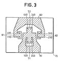
- Figure 3 shows a ceramic plate 15 serving as a cover for the housing 10 at the same time as the electrical connection surface of the input and output circuits of an amplifier whose active component consists of all four transistors .
- the starting and / or arrival areas of these circuits are materialized on the upper face of the housing cover, for example by metal conductors 60 and 70 which are, for example, strips of copper or golden nickel welded to the plate 15.
- This plate 15 itself comprises eight perforations passing right through the ceramic and the corresponding metal area. These perforations have been assigned marks 110, 210, 310 and 410 to recall those of the terminals of the base pins intended to pass through them, and marks 140, 240, 340 and 440 to recall those of the terminals of the collector pins intended for cross them, when the housing is closed using the plate 15 for this purpose.
- the latter also comprises, on the periphery of its face opposite to the conductors 60 and 70, a metallization intended to allow welding with the edge of the housing 10 so as to seal the housing.
- the conductors 60 and 70 have complementary shapes, studied so as to group the pins into two sets of four: the perforations 110 to 410 are grouped two by two on two metal areas 61 and 62 symmetrical with respect to the center of the plate 15 and surround the conductor 70 where two areas 71 and 72 group the perforations 140 to 440 in pairs. This thus ensures the best possible reduction of the parasitic inductances in the case of a group of four transistors.
- the invention is applicable to power amplifiers, at very high frequency, using 2n transistors. It suffices to store the transistors in n columns arranged on the first plate on individual plates provided with terminals and pins similar to those of the device with 4 transistors.
- the metal pads are arranged analogously to that of FIG. 3.
- the invention is applicable to field effect transistors in which the electrodes placed in parallel are on the one hand the grids and on the other hand the drains, the sources being brought to the
Landscapes
- Engineering & Computer Science (AREA)
- Power Engineering (AREA)
- Microelectronics & Electronic Packaging (AREA)
- Physics & Mathematics (AREA)
- Condensed Matter Physics & Semiconductors (AREA)
- General Physics & Mathematics (AREA)
- Computer Hardware Design (AREA)
- Microwave Amplifiers (AREA)
- Lead Frames For Integrated Circuits (AREA)
- Cooling Or The Like Of Semiconductors Or Solid State Devices (AREA)
- Bipolar Transistors (AREA)
Applications Claiming Priority (2)
| Application Number | Priority Date | Filing Date | Title |
|---|---|---|---|
| FR7928692A FR2470445A1 (fr) | 1979-11-21 | 1979-11-21 | Dispositif de mise en parallele de transistors bipolaires de puissance en tres haute frequence et amplificateur utilisant ce dispositif |
| FR7928692 | 1979-11-21 |
Publications (2)
| Publication Number | Publication Date |
|---|---|
| EP0030168A1 EP0030168A1 (fr) | 1981-06-10 |
| EP0030168B1 true EP0030168B1 (fr) | 1983-05-11 |
Family
ID=9231942
Family Applications (1)
| Application Number | Title | Priority Date | Filing Date |
|---|---|---|---|
| EP80401449A Expired EP0030168B1 (fr) | 1979-11-21 | 1980-10-09 | Dispositif de mise en parallèle de transistors de puissance en très haute fréquence |
Country Status (5)
| Country | Link |
|---|---|
| US (1) | US4408219A (OSRAM) |
| EP (1) | EP0030168B1 (OSRAM) |
| JP (1) | JPS5683960A (OSRAM) |
| DE (1) | DE3063167D1 (OSRAM) |
| FR (1) | FR2470445A1 (OSRAM) |
Families Citing this family (6)
| Publication number | Priority date | Publication date | Assignee | Title |
|---|---|---|---|---|
| NL8601743A (nl) * | 1985-07-05 | 1987-02-02 | Acrian Inc | Transistorpakket. |
| US4639760A (en) * | 1986-01-21 | 1987-01-27 | Motorola, Inc. | High power RF transistor assembly |
| JPH088269B2 (ja) * | 1986-10-22 | 1996-01-29 | シーメンス、アクチエンゲゼルシヤフト | 半導体デバイス |
| USRE34395E (en) * | 1989-06-15 | 1993-10-05 | Cray Research, Inc. | Method of making a chip carrier with terminating resistive elements |
| US6297700B1 (en) * | 2000-02-18 | 2001-10-02 | Ultrarf, Inc. | RF power transistor having cascaded cells with phase matching between cells |
| EP1596436A1 (en) * | 2004-05-12 | 2005-11-16 | Seiko Epson Corporation | Electronic circuit and method for manufacturing an electronic circuit |
Family Cites Families (4)
| Publication number | Priority date | Publication date | Assignee | Title |
|---|---|---|---|---|
| BE760031A (fr) * | 1969-12-11 | 1971-05-17 | Rca Corp | Boitier pour module de puissance hybride a semiconducteurs |
| DE7512573U (de) * | 1975-04-19 | 1975-09-04 | Semikron Gesellschaft Fuer Gleichri | Halbleitergleichrichteranordnung |
| DE2731211A1 (de) * | 1977-07-11 | 1979-01-25 | Semikron Gleichrichterbau | Halbleiterbaueinheit |
| US4296456A (en) * | 1980-06-02 | 1981-10-20 | Burroughs Corporation | Electronic package for high density integrated circuits |
-
1979
- 1979-11-21 FR FR7928692A patent/FR2470445A1/fr active Granted
-
1980
- 1980-10-09 EP EP80401449A patent/EP0030168B1/fr not_active Expired
- 1980-10-09 DE DE8080401449T patent/DE3063167D1/de not_active Expired
- 1980-11-18 US US06/208,006 patent/US4408219A/en not_active Expired - Lifetime
- 1980-11-20 JP JP16400280A patent/JPS5683960A/ja active Pending
Also Published As
| Publication number | Publication date |
|---|---|
| FR2470445A1 (fr) | 1981-05-29 |
| FR2470445B1 (OSRAM) | 1983-04-29 |
| JPS5683960A (en) | 1981-07-08 |
| EP0030168A1 (fr) | 1981-06-10 |
| DE3063167D1 (en) | 1983-06-16 |
| US4408219A (en) | 1983-10-04 |
Similar Documents
| Publication | Publication Date | Title |
|---|---|---|
| EP0228953B1 (fr) | Boîtier d'encapsulation d'un circuit électronique | |
| US7335835B2 (en) | Solar cell structure with by-pass diode and wrapped front-side diode interconnection | |
| FR2621173A1 (fr) | Boitier pour circuit integre de haute densite | |
| EP0133125B1 (fr) | Boîtier de composant électronique muni d'un condensateur | |
| US3958195A (en) | R.f. transistor package having an isolated common lead | |
| FR2609841A1 (fr) | Dispositif de circuit integre a semi-conducteurs | |
| FR2606206A1 (fr) | Condensateur de decouplage pour module a reseau d'ergots en grille | |
| US4209347A (en) | Mounting for solar cell | |
| US3965568A (en) | Process for fabrication and assembly of semiconductor devices | |
| FR2816112A1 (fr) | Moule a semi-conducteurs | |
| EP0030168B1 (fr) | Dispositif de mise en parallèle de transistors de puissance en très haute fréquence | |
| US4881117A (en) | Semiconductor power device formed of a multiplicity of identical parallel-connected elements | |
| EP0353114B1 (fr) | Dispositif d'interconnexion entre un circuit intégré et un circuit électrique et procédé de fabrication du dispositif | |
| US3479570A (en) | Encapsulation and connection structure for high power and high frequency semiconductor devices | |
| US4241360A (en) | Series capacitor voltage multiplier circuit with top connected rectifiers | |
| EP0446125B1 (fr) | Composant semi-conducteur de puissance | |
| EP0166634B1 (fr) | Dispositif de répartition de potentiel électrique, et boîtier de composant électronique incorporant un tel dispositif | |
| FR2693031A1 (fr) | Dispositif à semiconducteurs, substrat et cadre de montage pour ce dispositif. | |
| FR2632477A1 (fr) | Connecteur actif pour carte de circuits imprimes | |
| US4859851A (en) | Thermal-radiation imaging devices and systems, and the manufacture of such imaging devices | |
| FR2618944A1 (fr) | Dispositif a semi-conducteur encapsule dans un boitier comprenant un support metallique et un corps en resine synthetique | |
| EP0079265A1 (fr) | Procédé de réalisation d'un socle pour le montage d'une pastille semiconductrice sur l'embase d'un boîtier d'encapsulation | |
| FR2790905A1 (fr) | Composant electrique de puissance a montage par brasage sur un support et procede de montage correspondant | |
| EP0282396A1 (fr) | Structure de circuit hybride complexe et procédé de fabrication | |
| EP0020787B1 (en) | High frequency semiconductor unit |
Legal Events
| Date | Code | Title | Description |
|---|---|---|---|
| PUAI | Public reference made under article 153(3) epc to a published international application that has entered the european phase |
Free format text: ORIGINAL CODE: 0009012 |
|
| AK | Designated contracting states |
Designated state(s): DE GB IT NL |
|
| 17P | Request for examination filed |
Effective date: 19810624 |
|
| ITF | It: translation for a ep patent filed | ||
| GRAA | (expected) grant |
Free format text: ORIGINAL CODE: 0009210 |
|
| AK | Designated contracting states |
Designated state(s): DE GB IT NL |
|
| REF | Corresponds to: |
Ref document number: 3063167 Country of ref document: DE Date of ref document: 19830616 |
|
| PLBE | No opposition filed within time limit |
Free format text: ORIGINAL CODE: 0009261 |
|
| STAA | Information on the status of an ep patent application or granted ep patent |
Free format text: STATUS: NO OPPOSITION FILED WITHIN TIME LIMIT |
|
| 26N | No opposition filed | ||
| PGFP | Annual fee paid to national office [announced via postgrant information from national office to epo] |
Ref country code: NL Payment date: 19901031 Year of fee payment: 11 |
|
| ITTA | It: last paid annual fee | ||
| PG25 | Lapsed in a contracting state [announced via postgrant information from national office to epo] |
Ref country code: NL Effective date: 19920501 |
|
| NLV4 | Nl: lapsed or anulled due to non-payment of the annual fee | ||
| PGFP | Annual fee paid to national office [announced via postgrant information from national office to epo] |
Ref country code: GB Payment date: 19991006 Year of fee payment: 20 |
|
| PGFP | Annual fee paid to national office [announced via postgrant information from national office to epo] |
Ref country code: DE Payment date: 19991008 Year of fee payment: 20 |
|
| PG25 | Lapsed in a contracting state [announced via postgrant information from national office to epo] |
Ref country code: GB Free format text: LAPSE BECAUSE OF EXPIRATION OF PROTECTION Effective date: 20001008 |
|
| REG | Reference to a national code |
Ref country code: GB Ref legal event code: PE20 Effective date: 20001008 |