EP0029923B1 - Circuit de commande de mémoire tampon - Google Patents
Circuit de commande de mémoire tampon Download PDFInfo
- Publication number
- EP0029923B1 EP0029923B1 EP80106693A EP80106693A EP0029923B1 EP 0029923 B1 EP0029923 B1 EP 0029923B1 EP 80106693 A EP80106693 A EP 80106693A EP 80106693 A EP80106693 A EP 80106693A EP 0029923 B1 EP0029923 B1 EP 0029923B1
- Authority
- EP
- European Patent Office
- Prior art keywords
- counter
- count
- input
- buffer
- control circuit
- Prior art date
- Legal status (The legal status is an assumption and is not a legal conclusion. Google has not performed a legal analysis and makes no representation as to the accuracy of the status listed.)
- Expired
Links
Images

Classifications
-
- G—PHYSICS
- G06—COMPUTING OR CALCULATING; COUNTING
- G06K—GRAPHICAL DATA READING; PRESENTATION OF DATA; RECORD CARRIERS; HANDLING RECORD CARRIERS
- G06K7/00—Methods or arrangements for sensing record carriers, e.g. for reading patterns
- G06K7/10—Methods or arrangements for sensing record carriers, e.g. for reading patterns by electromagnetic radiation, e.g. optical sensing; by corpuscular radiation
- G06K7/10544—Methods or arrangements for sensing record carriers, e.g. for reading patterns by electromagnetic radiation, e.g. optical sensing; by corpuscular radiation by scanning of the records by radiation in the optical part of the electromagnetic spectrum
- G06K7/10821—Methods or arrangements for sensing record carriers, e.g. for reading patterns by electromagnetic radiation, e.g. optical sensing; by corpuscular radiation by scanning of the records by radiation in the optical part of the electromagnetic spectrum further details of bar or optical code scanning devices
- G06K7/10851—Circuits for pulse shaping, amplifying, eliminating noise signals, checking the function of the sensing device
-
- G—PHYSICS
- G06—COMPUTING OR CALCULATING; COUNTING
- G06K—GRAPHICAL DATA READING; PRESENTATION OF DATA; RECORD CARRIERS; HANDLING RECORD CARRIERS
- G06K7/00—Methods or arrangements for sensing record carriers, e.g. for reading patterns
- G06K7/01—Details
- G06K7/016—Synchronisation of sensing process
- G06K7/0166—Synchronisation of sensing process by means of clock-signals derived from the code marks, e.g. self-clocking code
Definitions
- the present invention relates to a buffer memory control circuit as defined by claim 1 and, more particularly, such a circuit usable in an optical analyzer.
- a well-known type of analyzer which makes it possible to read labels comprising information coded by means of a bar code such as that called in the Anglo-Saxon literature "Universal Product Code” (UPC), repeatedly scans the product on which the label is located by means of a coherent beam of light when the product passes in front of an appropriate window.
- the light which is reflected inside this window changes intensity depending on the reflecting power of the part of the surface which is struck by the beam.
- an irregular sinusoid is obtained having positive and negative peaks.
- the length of the positive and negative parts of the signal is proportional to the width of the light and dark bars that the label contains when the latter is actually struck by the beam.
- the analysis of a label containing information thus coded is made more complicated by the fact that the surface of the product which is located near the label generally comprises printed symbols or designs which, when scanned by the light beam, cause the generation of irregular sinusoidal signals. It is therefore necessary for the analyzer to be able to distinguish between these latter signals, which are irrelevant from the point of view of decoding, and the sinusoidal signals which are representative of the coded data which the label contains.
- the devices of the prior art In order to minimize the amount of raw data that it is necessary to decode, the devices of the prior art generally include selection or discrimination circuits which examine the signals generated by the analyzer, one word at a time, as the data represented by these signals are loaded into a buffer memory. When it results from this examination that the buffer contains data which probably relate to the content of the label, this data is transmitted to a processor, generally by means of an interrupt routine, for the purposes of analysis. more detailed. The buffer memory thus freed of its content can then receive new signals generated by the analyzer.
- the logic tests carried out by the logic selection circuits are of a crude nature, that is to say less rigorous than those carried out by the processor.
- Another solution would be to carry out a minimum of coarse tests or not to carry out any coarse test, almost all of the raw data supplied by the analyzer then being transmitted to a processor for the purpose of a rigorous analysis.
- the disadvantage of this solution is that it would require a very large part of the total operating time of the processor to be spent sorting through considerable amounts of raw data generated during the operation of the analyzer so as to separate relatively few data that actually relate to the content of a label from other data, which is meaningless. Since the processor is generally used for supervision or calculation purposes, this would necessarily result in a degradation of the system response time. To obtain an acceptable response time, it would probably be necessary to use an expensive and more powerful processor.
- the present invention relates to a buffer memory control circuit which makes it possible to save, with a view to their subsequent transfer to a processor, all the data identified by logical selection circuits as being potentially valid data, that is to say capable of relating to the content of a label, while rejecting most of the other raw data generated by the 'analyzer. Said circuit also makes it possible to reduce the time that the processor must devote to a more detailed analysis and to the decoding of the data.
- a control circuit produced in accordance with the present invention is used with several data storage devices, one of which is chosen to be always active, that is to say set to store data elements received in series .
- the control circuit comprises means making it possible to examine these elements and to generate a so-called “potentially valid data” (DPV) signal when a first number of said elements satisfies predetermined criteria; it also includes means for counting the data elements until a value corresponding to this first number is reached and for maintaining this value unless or until a DPV signal is generated.
- a switching device allows, when a second number of data elements greater than said first number is reached, to put a data storage device, previously rendered inactive, in a state to receive subsequent data elements. The data in the storage device previously made active is transferred to a processor for detailed analysis.
- a label reading device in which the present invention can be used and which comprises an analyzer 10.
- the latter which may be of a conventional type, preferably comprises a laser, elements beam deflection which make it possible to generate a scanning configuration by means of the laser beam, conversion circuits making it possible to obtain an electrical signal which varies according to the intensity of the reflected light, as well as threshold circuits or other pulse shaping circuits which make it possible to obtain a train of square pulses from an irregular sinusoidal signal.
- This train of pulses is applied both to a transition detector 12 and to a counter 14.
- the function of the detector 12 is to provide a chronological signal coinciding with the appearance of the front edge of each positive pulse and of each negative pulse.
- the counter 14 generates a binary word whose value is a function of the width of each pulse.
- This counter preferably consists of a binary counter excited by an HF clock. The excitation of the counter coincides with the appearance of the front edge of each pulse and ends when the rear edge appears.
- the value of the counter output signal is directly proportional to the width of the pulses.
- the signals or binary words obtained at the output of the counter 14 are applied in parallel via a cable 16 to a logic selection circuit 18.
- the function of the latter is to examine the data it receives and to provide a potentially valid data signal (DPV) each time a predetermined number of successive words pass rough logic tests. Circuits of this type are described in particular in documents US-A-3,909,787 and 4,086,477.
- the DPV signal generated by circuit 18 is preferably multi-bit and indicates not only that potentially valid data has been found, but also the direction in which the label was scanned. This signal is added to one of the data words transmitted on the cable 16.
- said signal is not added to the last word in the potentially valid data block, but is separated from it by one or more data words. For example, if such a block consists of 20 words, said signal is added to the second word which follows this block, that is to say to the 22nd word. The value of this offset is fixed during the design of the device.
- the word thus obtained which consists of the combined outputs of the counter 14 and of the logic circuit 18, is applied to a pair of buffer memory control circuits 20 and 22 which will be described later.
- the function of each of these circuits is to control the storage of the data words received via the cable 16 in one or the other of two buffer memories, which are preferably identical, 24 and 26, is stored being carried out under the control of a buffer selection circuit 28.
- the latter which will be described later, operates itself even under the control of the input signals which it receives from circuit 18 and from detector 12.
- the selection circuit 28 also generates an output signal which is applied to a processor 30 when it turns out that one of the buffer memories is completely filled and contains potentially valid data.
- the circuit 28 while transmitting said signal to the processor 30, causes the storage of the data that is being received in the buffer memory which was previously inactive.
- the processor 30 controls a multiplexing circuit 32 so as to transport the data contained in the fully filled buffer memory.
- the data words received are directed via one of the control circuits 20, 22 to an active buffer memory while being examined by the selection circuit 18. If the active buffer memory is filled, the older data is replaced by newly received data.
- the logic circuit 28 finds that the active buffer memory is full and contains a potentially valid data block, the data words received are loaded into the buffer memory which was previously inactive and the processor 30 is informed accordingly, so that it can then begin to transfer the data from the fully loaded buffer memory via the multiplexer 32.
- the processor 30 then performs a more rigorous analysis of the data in order to definitively determine whether the latter actually relates to the content of a label.
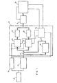
- FIG. 2 shows in more detail the buffer control circuits and the buffer selection circuit 28.
- This figure essentially comprises all the elements contained inside the dotted frame 34 of Figure 1.
- the signals whose l he origin lies outside this framework are identified by reference to the components from which they emanate.
- the buffer memories 24 and 26 are of the selective access or directly addressable type and include several memory positions, each of which can be addressed separately and contain a word of several bits.
- the number of memory positions in each buffer is greater than the number of words required to constitute a potentially valid block of data.
- the control circuit 20 relating to the buffer memory 24 comprises an address counter 36, the maximum value of which corresponds to the number of memory positions that the buffer memory comprises 24.
- the counter 36 is energized by means of the output of a door AND 38 with two inputs, one of which receives the output of a bistable device such as a flip-flop 40, which changes state each time a pulse is applied to its clock input (C), the other input of the AND gate 38 receiving the output of the transition detector 12.
- each transition of the signal supplied by the analyzer 10 makes the AND gate 38 pass. Therefore, the value of counter 36 is incremented by one so as to designate a new storage position for buffer memory 24.
- the inverted output of flip-flop 40 is also applied to one of the inputs of each.
- the AND gate assembly 42 transmits any which word supplied by the counter 14 and by the logic circuit 18 as long as the flip-flop 40 is in its restored state. The memory position to which the word is directed depends on the current output of counter 36.
- control circuit associated with the second buffer memory 26 is practically identical to the control circuit already described. More specifically, the control circuit of the buffer memory 26 comprises a self-restoring address counter 44 which is excited by the output of an AND gate 46 with two inputs, as well as a set 48 of AND gates each of which is connected to a different conductor contained in the cable 16 and has a common connection with the flip-flop 40.
- circuits 20 and 22 are controlled by the complementary outputs of the flip-flop 40.
- the AND gate 38 and the AND gates which the all 42 are turned on so that the data can be stored in the buffer memory 24 in sequentially addressed positions.
- the AND gates of the assembly 48 and the AND gate 46 are blocked by a low level signal emanating from the flip-flop 40 so that the buffer memory 26 cannot receive the data.
- the flip-flop 40 is in its opposite state (engaged)
- the AND gates associated with the buffer memory 26 are turned on and therefore the received data can be stored in positions of this buffer memory which are addressed in a manner sequential.
- the AND gates associated with the buffer memory 24 are blocked by a low level signal obtained at the inverted output of the flip-flop 40.
- the flip-flop 40 is one of the components of the buffer selection circuit 28.
- the state of this flip-flop is determined by a control counter 50, which is preferably a binary auto counter. restoration capable of reaching a maximum value corresponding to the number of memory positions that each of the buffer memories 24 and 26 comprises.
- the counter 50 is excited by means of pulses provided by an AND gate 52 with two inputs, one of which receives a pulse each time the transition detector 12 detects the leading edge of a positive or negative pulse emanating from the analyzer, the second input of AND gate 52 receiving, under conditions which will be specified later, the output of an OR gate 54 forming part of the buffer memory selection circuit 28.
- the output of the counter 50 is transmitted to two logic circuits 56 and 58.
- the latter can consist of sets of AND gates connected to particular stages of the counter 50 so that positive logic output signals are only generated when a first value and a second value of the counter are reached respectively.
- the logic circuit 56 has the function of recognizing the instant when the counter 50 has reached said first value, which corresponds to the number of words constituting the whole of a potentially valid data block plus the number of words representing the delay of the said signal. potentially valid data (DPV) and separating the generation of this from the last word of the block.
- DUV potentially valid data
- the logic 56 would be designed so as to detect the instant when the value forty-two would be reached.
- logic circuit 58 The function of logic circuit 58 is to detect a second value, corresponding to the maximum word storage capacity presented by the buffer memories 24 and 26. For example, if each of these memories had a capacity of 64 words of several bits, logic circuit 58 would provide a positive output when value 64 is reached.
- a restoration loop 60 makes it possible to reset the counter 50 to an initial value (preferably zero) once said second value has been detected.
- the output of logic circuit 58 is applied to the clock input (C) of the flip-flop 40, to the switching inputs (S) of two flip-flops 62 and 64, respectively, and to the restoration input ( R) of another flip-flop 66. As will be seen below, the counter 50 does not reach the second value until one of the buffer memories 24 and 26 is completely filled and contains a potentially block of data.
- the flip-flop 62 responds to the detection of said second value by transmitting an interrupt request signal to the processor 30 in order to cause the transfer of the data contained in the buffer memory to the processor via the multiplexer 32.
- the flip- flop 62 is restored by processor 30 when this transfer has been made.
- the flip-flop 64 is restored by the output generated by the logic circuit 56 when the first value is reached by the control counter 50, and is triggered by the output generated by the logic circuit 58 when the second value is reached. As a result, the flip-flop 64 provides a high level signal each time the value of the output of the counter 50 varies between the unit and said first value. If the values given above are used as examples, the flip-flop 64 generates a high level signal at all values from 1 to 42, and a low level signal at all values from 43 to 64. The output flip-flop 64 is applied to one of the inputs of an OR gate 54.
- the flip-flop 66 is triggered each time the selection logic circuit 18 detects a potentially valid data block and is restored when the second value is reached.
- the time interval during which the flip-flop 66 is activated or restored is undefined and can vary considerably from one operating cycle to another, depending solely on the moment when the block is detected.
- the logic components associated with counter 50 allow it to count until the first value is reached, if no potentially valid data block has been obtained.
- the counter is kept at this first value while the data corresponding to the signals that are being received continues to be loaded into the active buffer memory.
- the logic circuit 18 detects such a block, the counter 50 is incremented by one unit per word received until the second value has been reached, the flip-flop 40 then changing state to direct the words subsequently received. to the buffer that was previously inactive.
- the flip-flop 62 is triggered so that a signal is transmitted to the processor 30 so that the data is transferred to the latter, from the fully filled buffer memory, via the multi p lexer 32.
- the maximum capacity of each of the buffer memories 24 and 26 is 64 words, which corresponds to the second value, or maximum value, that the command counter 50 can reach. It is also assumed that a block of potentially valid data consists of forty words and that the DPV signal is separated from this block by two words, the first value therefore being equal to 42.
- the flip-flop 40 is initially restored in such a way that the AND gate 38 and the AND doors of the assembly 42 are partially passable.
- the address counter 36 is initially set to 1 in order to address the first memory position that comprises the buffer memory 24.
- the transition detector 12 When the circuit is energized, the transition detector 12 continuously seeks to determine the appearance of a transition. None happens until a transition has been detected. Otherwise, the word received is transmitted via the set 42 of AND gates to the first memory position of the buffer memory 26. The transition thus detected is also transmitted via the AND gate 38 to the address counter 36 of so as to increment the value of the address by one.
- the command counter 50 If the value of the command counter 50 is less than 42, this value is incremented by one and the process begins again. After the first transition, the counters 50 and 36 are at the value 1 and a word is stored in the buffer memory 24.
- This process is repeated at each transition of the received signal until it has been determined that the value of the counter 50 is at least equal to 42. It is then determined whether this value is greater than or equal to 42, but less than 64 If the value is between these limits, a check is made to determine if a potentially valid block of data has been found. If not, the process starts again. If, on the contrary, such a block was found during the current counting cycle (i.e. from 1 to the current value), the value of counter 50 is incremented before the process starts again.
- the steps which have just been described are repeated until the verification of the value of the counter 50 indicates that it is equal to 64, which indicates that one of the buffer memories is completely filled and contains at least a few words constituting potentially valid data.
- the counter 50 is then reset to 1 by means of the restoration loop 60.
- the flip-flop 40 is engaged so as to make active the control circuit 22 associated with the buffer memory 26.
- the flip flop 62 is engaged and transmits to the processor 30 a signal which causes the transfer to the processor of the data contained in the buffer memory 24.
- the buffer loading cycle is repeated as described, whether the active buffer is buffer 24 or 26. It will however be noted that, although the command counter 50 stops at the value 42 or is held at this value unless a potentially valid data selection pulse has been generated before the counter 50 has reached this value, the data words continue to be written to the buffer 26 cyclically, the most data are written to the memory location that contains the oldest data. The counter 50 can only exceed the value 42 when a pulse for selecting potentially valid data is generated during the current counting cycle.
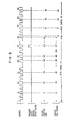
- Figure 3 shows the words received, a potentially valid data selection pulse, and the values of the control counter 50 and the buffer address counter during a single buffer load cycle.
- each positive pulse represents a black bar used on a label for data coding purposes and that each negative pulse represents a white bar (or space) on the same label.
- the value of the command counter and that of the address counter associated with the chosen buffer memory follow the number of data words received until the command counter reaches the first value, that is to say 42. If no potentially valid data selection pulse has been generated in the meantime, the two signals applied to the inputs of the OR gate 54 go to low level, which has the effect of blocking the AND gate 52 and preventing the application of other pulses to the counter 50.
- the address counter associated with the buffer memory 24 continues to be incremented at each transition so that the oldest data contained in the buffer memory can be replaced by the most recently received data .
- the flip-flop 66 When a potentially valid data selection pulse is finally generated, the flip-flop 66 is triggered and changes the output of the OR gate 54 to a high level. The command counter 50 then resumes counting the transitions, starting at the value 42. As long as the value 64 has not been reached, the data words received continue to be loaded into the buffer memory, the words stored most old ones being replaced by new words. When the value 64 is reached, the flip-flop 40 changes state and applies a signal to the AND gates associated with the buffer memory 26 which was previously inactive, these doors being turned on, while a signal is applied to the AND gates associated with the buffer memory 24, which is now completely filled, so as to block these latter doors.
- the address counter associated with the buffer memory 26 has been set to 1 either during startup, or after the last transfer of the content of the buffer memory to the processor 30.
- the command counter is also reset to 1 by the signal supplied by through its restore loop 60.
- the value of the command counter and that of the buffer address counter progress in an identical manner during the loading of the first 42 words of data into the buffer memory 26.
- the content of the buffer memory 34 is transferred to the processor 30 via the multiplexer 32.
- the storage control process relating to the buffer memory 26 is practically identical to that already described in the case of the buffer memory 24.
- the command counter 50 counts up to the value 42 and remains at this latter value unless the logic selection circuit 18 does not cause the flip-flop 66 to be triggered at a value between 1 and 42 to indicate that the buffer memory that is being loaded contains potentially valid data. If no potentially valid data signal is generated by the circuit 18 before the value 42 is reached, 42, the counter 50 remains at this value although the data words continue to be written in the buffer memory 26, the words the most recent ones replacing the oldest words. Counting resumes only when a pulse of potentially valid data causes the flip-flop 66 to engage.
- the advantage of this arrangement with two buffer memories is obvious.
- the processor 30 is only interrupted for the purpose of decoding when one of the buffer memories is completely filled and contains potentially valid data. No interruption occurs and a fully filled buffer does not contain potentially valid data or if a partially filled buffer contains such data.
- the data received is directed to another buffer memory when it has been found that the first contains potentially valid data, there is no loss of data even if the potentially valid data overlap or are nested.
Landscapes
- Physics & Mathematics (AREA)
- Engineering & Computer Science (AREA)
- Electromagnetism (AREA)
- Computer Vision & Pattern Recognition (AREA)
- General Physics & Mathematics (AREA)
- Theoretical Computer Science (AREA)
- Artificial Intelligence (AREA)
- Health & Medical Sciences (AREA)
- General Health & Medical Sciences (AREA)
- Toxicology (AREA)
- Complex Calculations (AREA)
- Time-Division Multiplex Systems (AREA)
- Synchronisation In Digital Transmission Systems (AREA)
Applications Claiming Priority (2)
| Application Number | Priority Date | Filing Date | Title |
|---|---|---|---|
| US06/098,461 US4344152A (en) | 1979-11-29 | 1979-11-29 | Buffer memory control circuit for label scanning system |
| US98461 | 1979-11-29 |
Publications (2)
| Publication Number | Publication Date |
|---|---|
| EP0029923A1 EP0029923A1 (fr) | 1981-06-10 |
| EP0029923B1 true EP0029923B1 (fr) | 1985-02-06 |
Family
ID=22269373
Family Applications (1)
| Application Number | Title | Priority Date | Filing Date |
|---|---|---|---|
| EP80106693A Expired EP0029923B1 (fr) | 1979-11-29 | 1980-10-31 | Circuit de commande de mémoire tampon |
Country Status (5)
| Country | Link |
|---|---|
| US (1) | US4344152A (enExample) |
| EP (1) | EP0029923B1 (enExample) |
| JP (1) | JPS5679371A (enExample) |
| CA (1) | CA1148259A (enExample) |
| DE (1) | DE3070126D1 (enExample) |
Families Citing this family (8)
| Publication number | Priority date | Publication date | Assignee | Title |
|---|---|---|---|---|
| US4500880A (en) * | 1981-07-06 | 1985-02-19 | Motorola, Inc. | Real time, computer-driven retail pricing display system |
| US4914623A (en) * | 1986-09-18 | 1990-04-03 | Hudson-Allen Limited | Digital processing of sensor signals for reading binary storage media |
| JPS63135827U (enExample) * | 1987-02-26 | 1988-09-06 | ||
| JP3313362B2 (ja) * | 1990-10-04 | 2002-08-12 | 日本電気株式会社 | 音声処理装置のメモリーアドレス発生器 |
| WO1993003455A1 (en) * | 1991-08-02 | 1993-02-18 | Intermec Corporation | Method and apparatus for scanning symbols |
| EP0831418B1 (en) * | 1991-10-21 | 2002-03-13 | Canon Kabushiki Kaisha | Method and apparatus for character recognition |
| AU3497497A (en) | 1996-06-21 | 1998-01-07 | Norand Corporation | Too long code reader performing coded image decoding |
| US20040064455A1 (en) * | 2002-09-26 | 2004-04-01 | Eastman Kodak Company | Software-floating palette for annotation of images that are viewable in a variety of organizational structures |
Family Cites Families (9)
| Publication number | Priority date | Publication date | Assignee | Title |
|---|---|---|---|---|
| US3752958A (en) * | 1971-12-07 | 1973-08-14 | Ncr | Field detection logic |
| US3868634A (en) | 1972-11-03 | 1975-02-25 | Scanner | Reading of contrasting data by means of continuously attempting to decode read signals |
| US3868636A (en) * | 1973-06-18 | 1975-02-25 | Isotec Inc | Optical character reader having feature recognition capability |
| US3909787A (en) * | 1974-07-01 | 1975-09-30 | Ibm | Candidate selection processor |
| JPS586982B2 (ja) * | 1976-08-18 | 1983-02-07 | 株式会社デンソー | バ−コ−ド読取方法および装置 |
| US4125765A (en) * | 1977-06-27 | 1978-11-14 | International Business Machines Corporation | Label find method and circuit |
| US4086477A (en) * | 1977-06-27 | 1978-04-25 | International Business Machines Corporation | Decoding method and circuit |
| US4162035A (en) * | 1977-09-23 | 1979-07-24 | General Signal Corporation | High resolution optical position code detector for information recorded on record carrier partially in humanly intelligible form |
| US4298954A (en) * | 1979-04-30 | 1981-11-03 | International Business Machines Corporation | Alternating data buffers when one buffer is empty and another buffer is variably full of data |
-
1979
- 1979-11-29 US US06/098,461 patent/US4344152A/en not_active Expired - Lifetime
-
1980
- 1980-09-12 JP JP12619380A patent/JPS5679371A/ja active Granted
- 1980-09-26 CA CA000361883A patent/CA1148259A/en not_active Expired
- 1980-10-31 EP EP80106693A patent/EP0029923B1/fr not_active Expired
- 1980-10-31 DE DE8080106693T patent/DE3070126D1/de not_active Expired
Also Published As
| Publication number | Publication date |
|---|---|
| JPS6113636B2 (enExample) | 1986-04-14 |
| DE3070126D1 (en) | 1985-03-21 |
| EP0029923A1 (fr) | 1981-06-10 |
| US4344152A (en) | 1982-08-10 |
| CA1148259A (en) | 1983-06-14 |
| JPS5679371A (en) | 1981-06-29 |
Similar Documents
| Publication | Publication Date | Title |
|---|---|---|
| EP0023271B1 (fr) | Clavier d'entrée de données à touches à impédance variable contrôlé par microprocesseur | |
| FR92366E (enExample) | ||
| CA2191787C (fr) | Procede d'interrogation a distance d'etiquettes, station et etiquette pour sa mise en oeuvre | |
| EP0104293B1 (fr) | Dispositif pour le chargement et la lecture de différentes chaînes de bascules dans un système de traitement de données | |
| EP0967573B1 (fr) | Dispositif de traitement de données d'acquisition, notamment de données d'image | |
| EP0022004B1 (fr) | Procédé pour la commande de rapprochement à effectuer entre des entités logiques de référence et des entités logiques issues d'un fichier | |
| EP0020983B1 (fr) | Système de mémoire comportant un dispositif d'emmagasinage sérié | |
| EP0029923B1 (fr) | Circuit de commande de mémoire tampon | |
| BE897586A (fr) | Circuit parallele de controle de redondance cyclique | |
| FR2635207A1 (fr) | Procede et dispositif de traitement d'un signal electrique analogique en vue d'obtenir un signal binaire parametrable representatif de sa composante significative | |
| CH629319A5 (fr) | Installation de traitement de donnees. | |
| FR2533091A1 (fr) | Systeme de detection et de correction d'erreurs de transmission d'un message binaire utilisant un code cyclique detecteur et correcteur d'erreurs de type reed-solomon entrelace | |
| FR2666425A1 (fr) | Procede et dispositif de mise a jour d'informations dans une memoire et leur utilisation dans les cartes a memoire. | |
| FR2602070A1 (fr) | Systeme et procede d'acces a une memoire d'ordinateur. | |
| FR2572823A1 (fr) | Dispositif de lecture pour code a barres | |
| WO2010070594A2 (fr) | Capteur matriciel | |
| FR2468240A1 (fr) | Relais de telecommande | |
| FR2473753A1 (fr) | Dispositif pour fournir des groupes de donnees corriges a un circuit de destination | |
| EP0400520B1 (fr) | Dispositif de détection de perte de signal de réception pour récepteur de signaux numériques | |
| EP0367345B1 (fr) | Analyseur logique avec double déclenchement | |
| EP0633457A1 (fr) | Elément photosensible et dispositif pour la détection d'impulsions lumineuses | |
| EP0833346B1 (fr) | Mémoire à accès série avec sécurisation de l'écriture | |
| EP0012880A1 (fr) | Procédé de décodage de données binaires codées en phase, modulation de fréquence et modulation de fréquence modifiée | |
| FR2599525A1 (fr) | Unite a clavier de securite, en particulier pour la composition d'un code confidentiel | |
| FR2569068A1 (fr) | Appareil de decodage de codes d'image obtenus par un processus de compression |
Legal Events
| Date | Code | Title | Description |
|---|---|---|---|
| PUAI | Public reference made under article 153(3) epc to a published international application that has entered the european phase |
Free format text: ORIGINAL CODE: 0009012 |
|
| AK | Designated contracting states |
Designated state(s): CH DE FR GB IT NL |
|
| 17P | Request for examination filed |
Effective date: 19810706 |
|
| ITF | It: translation for a ep patent filed | ||
| GRAA | (expected) grant |
Free format text: ORIGINAL CODE: 0009210 |
|
| AK | Designated contracting states |
Designated state(s): CH DE FR GB IT LI NL |
|
| PG25 | Lapsed in a contracting state [announced via postgrant information from national office to epo] |
Ref country code: NL Effective date: 19850206 |
|
| REF | Corresponds to: |
Ref document number: 3070126 Country of ref document: DE Date of ref document: 19850321 |
|
| NLV1 | Nl: lapsed or annulled due to failure to fulfill the requirements of art. 29p and 29m of the patents act | ||
| PG25 | Lapsed in a contracting state [announced via postgrant information from national office to epo] |
Ref country code: LI Effective date: 19851031 Ref country code: CH Effective date: 19851031 |
|
| PLBE | No opposition filed within time limit |
Free format text: ORIGINAL CODE: 0009261 |
|
| STAA | Information on the status of an ep patent application or granted ep patent |
Free format text: STATUS: NO OPPOSITION FILED WITHIN TIME LIMIT |
|
| 26N | No opposition filed | ||
| REG | Reference to a national code |
Ref country code: CH Ref legal event code: PL |
|
| PGFP | Annual fee paid to national office [announced via postgrant information from national office to epo] |
Ref country code: GB Payment date: 19900911 Year of fee payment: 11 |
|
| PGFP | Annual fee paid to national office [announced via postgrant information from national office to epo] |
Ref country code: DE Payment date: 19901027 Year of fee payment: 11 |
|
| PGFP | Annual fee paid to national office [announced via postgrant information from national office to epo] |
Ref country code: FR Payment date: 19911001 Year of fee payment: 12 |
|
| ITTA | It: last paid annual fee | ||
| PG25 | Lapsed in a contracting state [announced via postgrant information from national office to epo] |
Ref country code: GB Effective date: 19911031 |
|
| GBPC | Gb: european patent ceased through non-payment of renewal fee | ||
| PG25 | Lapsed in a contracting state [announced via postgrant information from national office to epo] |
Ref country code: DE Effective date: 19920701 |
|
| PG25 | Lapsed in a contracting state [announced via postgrant information from national office to epo] |
Ref country code: FR Effective date: 19930630 |
|
| REG | Reference to a national code |
Ref country code: FR Ref legal event code: ST |