EP0029923B1 - Buffer memory control circuit - Google Patents
Buffer memory control circuit Download PDFInfo
- Publication number
- EP0029923B1 EP0029923B1 EP80106693A EP80106693A EP0029923B1 EP 0029923 B1 EP0029923 B1 EP 0029923B1 EP 80106693 A EP80106693 A EP 80106693A EP 80106693 A EP80106693 A EP 80106693A EP 0029923 B1 EP0029923 B1 EP 0029923B1
- Authority
- EP
- European Patent Office
- Prior art keywords
- counter
- count
- input
- buffer
- control circuit
- Prior art date
- Legal status (The legal status is an assumption and is not a legal conclusion. Google has not performed a legal analysis and makes no representation as to the accuracy of the status listed.)
- Expired
Links
Images

Classifications
-
- G—PHYSICS
- G06—COMPUTING; CALCULATING OR COUNTING
- G06K—GRAPHICAL DATA READING; PRESENTATION OF DATA; RECORD CARRIERS; HANDLING RECORD CARRIERS
- G06K7/00—Methods or arrangements for sensing record carriers, e.g. for reading patterns
- G06K7/10—Methods or arrangements for sensing record carriers, e.g. for reading patterns by electromagnetic radiation, e.g. optical sensing; by corpuscular radiation
- G06K7/10544—Methods or arrangements for sensing record carriers, e.g. for reading patterns by electromagnetic radiation, e.g. optical sensing; by corpuscular radiation by scanning of the records by radiation in the optical part of the electromagnetic spectrum
- G06K7/10821—Methods or arrangements for sensing record carriers, e.g. for reading patterns by electromagnetic radiation, e.g. optical sensing; by corpuscular radiation by scanning of the records by radiation in the optical part of the electromagnetic spectrum further details of bar or optical code scanning devices
- G06K7/10851—Circuits for pulse shaping, amplifying, eliminating noise signals, checking the function of the sensing device
-
- G—PHYSICS
- G06—COMPUTING; CALCULATING OR COUNTING
- G06K—GRAPHICAL DATA READING; PRESENTATION OF DATA; RECORD CARRIERS; HANDLING RECORD CARRIERS
- G06K7/00—Methods or arrangements for sensing record carriers, e.g. for reading patterns
- G06K7/01—Details
- G06K7/016—Synchronisation of sensing process
- G06K7/0166—Synchronisation of sensing process by means of clock-signals derived from the code marks, e.g. self-clocking code
Definitions
- the present invention relates to a buffer memory control circuit as defined by claim 1 and, more particularly, such a circuit usable in an optical analyzer.
- a well-known type of analyzer which makes it possible to read labels comprising information coded by means of a bar code such as that called in the Anglo-Saxon literature "Universal Product Code” (UPC), repeatedly scans the product on which the label is located by means of a coherent beam of light when the product passes in front of an appropriate window.
- the light which is reflected inside this window changes intensity depending on the reflecting power of the part of the surface which is struck by the beam.
- an irregular sinusoid is obtained having positive and negative peaks.
- the length of the positive and negative parts of the signal is proportional to the width of the light and dark bars that the label contains when the latter is actually struck by the beam.
- the analysis of a label containing information thus coded is made more complicated by the fact that the surface of the product which is located near the label generally comprises printed symbols or designs which, when scanned by the light beam, cause the generation of irregular sinusoidal signals. It is therefore necessary for the analyzer to be able to distinguish between these latter signals, which are irrelevant from the point of view of decoding, and the sinusoidal signals which are representative of the coded data which the label contains.
- the devices of the prior art In order to minimize the amount of raw data that it is necessary to decode, the devices of the prior art generally include selection or discrimination circuits which examine the signals generated by the analyzer, one word at a time, as the data represented by these signals are loaded into a buffer memory. When it results from this examination that the buffer contains data which probably relate to the content of the label, this data is transmitted to a processor, generally by means of an interrupt routine, for the purposes of analysis. more detailed. The buffer memory thus freed of its content can then receive new signals generated by the analyzer.
- the logic tests carried out by the logic selection circuits are of a crude nature, that is to say less rigorous than those carried out by the processor.
- Another solution would be to carry out a minimum of coarse tests or not to carry out any coarse test, almost all of the raw data supplied by the analyzer then being transmitted to a processor for the purpose of a rigorous analysis.
- the disadvantage of this solution is that it would require a very large part of the total operating time of the processor to be spent sorting through considerable amounts of raw data generated during the operation of the analyzer so as to separate relatively few data that actually relate to the content of a label from other data, which is meaningless. Since the processor is generally used for supervision or calculation purposes, this would necessarily result in a degradation of the system response time. To obtain an acceptable response time, it would probably be necessary to use an expensive and more powerful processor.
- the present invention relates to a buffer memory control circuit which makes it possible to save, with a view to their subsequent transfer to a processor, all the data identified by logical selection circuits as being potentially valid data, that is to say capable of relating to the content of a label, while rejecting most of the other raw data generated by the 'analyzer. Said circuit also makes it possible to reduce the time that the processor must devote to a more detailed analysis and to the decoding of the data.
- a control circuit produced in accordance with the present invention is used with several data storage devices, one of which is chosen to be always active, that is to say set to store data elements received in series .
- the control circuit comprises means making it possible to examine these elements and to generate a so-called “potentially valid data” (DPV) signal when a first number of said elements satisfies predetermined criteria; it also includes means for counting the data elements until a value corresponding to this first number is reached and for maintaining this value unless or until a DPV signal is generated.
- a switching device allows, when a second number of data elements greater than said first number is reached, to put a data storage device, previously rendered inactive, in a state to receive subsequent data elements. The data in the storage device previously made active is transferred to a processor for detailed analysis.
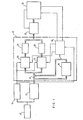
- a label reading device in which the present invention can be used and which comprises an analyzer 10.
- the latter which may be of a conventional type, preferably comprises a laser, elements beam deflection which make it possible to generate a scanning configuration by means of the laser beam, conversion circuits making it possible to obtain an electrical signal which varies according to the intensity of the reflected light, as well as threshold circuits or other pulse shaping circuits which make it possible to obtain a train of square pulses from an irregular sinusoidal signal.
- This train of pulses is applied both to a transition detector 12 and to a counter 14.
- the function of the detector 12 is to provide a chronological signal coinciding with the appearance of the front edge of each positive pulse and of each negative pulse.
- the counter 14 generates a binary word whose value is a function of the width of each pulse.
- This counter preferably consists of a binary counter excited by an HF clock. The excitation of the counter coincides with the appearance of the front edge of each pulse and ends when the rear edge appears.
- the value of the counter output signal is directly proportional to the width of the pulses.
- the signals or binary words obtained at the output of the counter 14 are applied in parallel via a cable 16 to a logic selection circuit 18.
- the function of the latter is to examine the data it receives and to provide a potentially valid data signal (DPV) each time a predetermined number of successive words pass rough logic tests. Circuits of this type are described in particular in documents US-A-3,909,787 and 4,086,477.
- the DPV signal generated by circuit 18 is preferably multi-bit and indicates not only that potentially valid data has been found, but also the direction in which the label was scanned. This signal is added to one of the data words transmitted on the cable 16.
- said signal is not added to the last word in the potentially valid data block, but is separated from it by one or more data words. For example, if such a block consists of 20 words, said signal is added to the second word which follows this block, that is to say to the 22nd word. The value of this offset is fixed during the design of the device.
- the word thus obtained which consists of the combined outputs of the counter 14 and of the logic circuit 18, is applied to a pair of buffer memory control circuits 20 and 22 which will be described later.
- the function of each of these circuits is to control the storage of the data words received via the cable 16 in one or the other of two buffer memories, which are preferably identical, 24 and 26, is stored being carried out under the control of a buffer selection circuit 28.
- the latter which will be described later, operates itself even under the control of the input signals which it receives from circuit 18 and from detector 12.
- the selection circuit 28 also generates an output signal which is applied to a processor 30 when it turns out that one of the buffer memories is completely filled and contains potentially valid data.
- the circuit 28 while transmitting said signal to the processor 30, causes the storage of the data that is being received in the buffer memory which was previously inactive.
- the processor 30 controls a multiplexing circuit 32 so as to transport the data contained in the fully filled buffer memory.
- the data words received are directed via one of the control circuits 20, 22 to an active buffer memory while being examined by the selection circuit 18. If the active buffer memory is filled, the older data is replaced by newly received data.
- the logic circuit 28 finds that the active buffer memory is full and contains a potentially valid data block, the data words received are loaded into the buffer memory which was previously inactive and the processor 30 is informed accordingly, so that it can then begin to transfer the data from the fully loaded buffer memory via the multiplexer 32.
- the processor 30 then performs a more rigorous analysis of the data in order to definitively determine whether the latter actually relates to the content of a label.
- FIG. 2 shows in more detail the buffer control circuits and the buffer selection circuit 28.
- This figure essentially comprises all the elements contained inside the dotted frame 34 of Figure 1.
- the signals whose l he origin lies outside this framework are identified by reference to the components from which they emanate.
- the buffer memories 24 and 26 are of the selective access or directly addressable type and include several memory positions, each of which can be addressed separately and contain a word of several bits.
- the number of memory positions in each buffer is greater than the number of words required to constitute a potentially valid block of data.
- the control circuit 20 relating to the buffer memory 24 comprises an address counter 36, the maximum value of which corresponds to the number of memory positions that the buffer memory comprises 24.
- the counter 36 is energized by means of the output of a door AND 38 with two inputs, one of which receives the output of a bistable device such as a flip-flop 40, which changes state each time a pulse is applied to its clock input (C), the other input of the AND gate 38 receiving the output of the transition detector 12.
- each transition of the signal supplied by the analyzer 10 makes the AND gate 38 pass. Therefore, the value of counter 36 is incremented by one so as to designate a new storage position for buffer memory 24.
- the inverted output of flip-flop 40 is also applied to one of the inputs of each.
- the AND gate assembly 42 transmits any which word supplied by the counter 14 and by the logic circuit 18 as long as the flip-flop 40 is in its restored state. The memory position to which the word is directed depends on the current output of counter 36.
- control circuit associated with the second buffer memory 26 is practically identical to the control circuit already described. More specifically, the control circuit of the buffer memory 26 comprises a self-restoring address counter 44 which is excited by the output of an AND gate 46 with two inputs, as well as a set 48 of AND gates each of which is connected to a different conductor contained in the cable 16 and has a common connection with the flip-flop 40.
- circuits 20 and 22 are controlled by the complementary outputs of the flip-flop 40.
- the AND gate 38 and the AND gates which the all 42 are turned on so that the data can be stored in the buffer memory 24 in sequentially addressed positions.
- the AND gates of the assembly 48 and the AND gate 46 are blocked by a low level signal emanating from the flip-flop 40 so that the buffer memory 26 cannot receive the data.
- the flip-flop 40 is in its opposite state (engaged)
- the AND gates associated with the buffer memory 26 are turned on and therefore the received data can be stored in positions of this buffer memory which are addressed in a manner sequential.
- the AND gates associated with the buffer memory 24 are blocked by a low level signal obtained at the inverted output of the flip-flop 40.
- the flip-flop 40 is one of the components of the buffer selection circuit 28.
- the state of this flip-flop is determined by a control counter 50, which is preferably a binary auto counter. restoration capable of reaching a maximum value corresponding to the number of memory positions that each of the buffer memories 24 and 26 comprises.
- the counter 50 is excited by means of pulses provided by an AND gate 52 with two inputs, one of which receives a pulse each time the transition detector 12 detects the leading edge of a positive or negative pulse emanating from the analyzer, the second input of AND gate 52 receiving, under conditions which will be specified later, the output of an OR gate 54 forming part of the buffer memory selection circuit 28.
- the output of the counter 50 is transmitted to two logic circuits 56 and 58.
- the latter can consist of sets of AND gates connected to particular stages of the counter 50 so that positive logic output signals are only generated when a first value and a second value of the counter are reached respectively.
- the logic circuit 56 has the function of recognizing the instant when the counter 50 has reached said first value, which corresponds to the number of words constituting the whole of a potentially valid data block plus the number of words representing the delay of the said signal. potentially valid data (DPV) and separating the generation of this from the last word of the block.
- DUV potentially valid data
- the logic 56 would be designed so as to detect the instant when the value forty-two would be reached.
- logic circuit 58 The function of logic circuit 58 is to detect a second value, corresponding to the maximum word storage capacity presented by the buffer memories 24 and 26. For example, if each of these memories had a capacity of 64 words of several bits, logic circuit 58 would provide a positive output when value 64 is reached.
- a restoration loop 60 makes it possible to reset the counter 50 to an initial value (preferably zero) once said second value has been detected.
- the output of logic circuit 58 is applied to the clock input (C) of the flip-flop 40, to the switching inputs (S) of two flip-flops 62 and 64, respectively, and to the restoration input ( R) of another flip-flop 66. As will be seen below, the counter 50 does not reach the second value until one of the buffer memories 24 and 26 is completely filled and contains a potentially block of data.
- the flip-flop 62 responds to the detection of said second value by transmitting an interrupt request signal to the processor 30 in order to cause the transfer of the data contained in the buffer memory to the processor via the multiplexer 32.
- the flip- flop 62 is restored by processor 30 when this transfer has been made.
- the flip-flop 64 is restored by the output generated by the logic circuit 56 when the first value is reached by the control counter 50, and is triggered by the output generated by the logic circuit 58 when the second value is reached. As a result, the flip-flop 64 provides a high level signal each time the value of the output of the counter 50 varies between the unit and said first value. If the values given above are used as examples, the flip-flop 64 generates a high level signal at all values from 1 to 42, and a low level signal at all values from 43 to 64. The output flip-flop 64 is applied to one of the inputs of an OR gate 54.
- the flip-flop 66 is triggered each time the selection logic circuit 18 detects a potentially valid data block and is restored when the second value is reached.
- the time interval during which the flip-flop 66 is activated or restored is undefined and can vary considerably from one operating cycle to another, depending solely on the moment when the block is detected.
- the logic components associated with counter 50 allow it to count until the first value is reached, if no potentially valid data block has been obtained.
- the counter is kept at this first value while the data corresponding to the signals that are being received continues to be loaded into the active buffer memory.
- the logic circuit 18 detects such a block, the counter 50 is incremented by one unit per word received until the second value has been reached, the flip-flop 40 then changing state to direct the words subsequently received. to the buffer that was previously inactive.
- the flip-flop 62 is triggered so that a signal is transmitted to the processor 30 so that the data is transferred to the latter, from the fully filled buffer memory, via the multi p lexer 32.
- the maximum capacity of each of the buffer memories 24 and 26 is 64 words, which corresponds to the second value, or maximum value, that the command counter 50 can reach. It is also assumed that a block of potentially valid data consists of forty words and that the DPV signal is separated from this block by two words, the first value therefore being equal to 42.
- the flip-flop 40 is initially restored in such a way that the AND gate 38 and the AND doors of the assembly 42 are partially passable.
- the address counter 36 is initially set to 1 in order to address the first memory position that comprises the buffer memory 24.
- the transition detector 12 When the circuit is energized, the transition detector 12 continuously seeks to determine the appearance of a transition. None happens until a transition has been detected. Otherwise, the word received is transmitted via the set 42 of AND gates to the first memory position of the buffer memory 26. The transition thus detected is also transmitted via the AND gate 38 to the address counter 36 of so as to increment the value of the address by one.
- the command counter 50 If the value of the command counter 50 is less than 42, this value is incremented by one and the process begins again. After the first transition, the counters 50 and 36 are at the value 1 and a word is stored in the buffer memory 24.
- This process is repeated at each transition of the received signal until it has been determined that the value of the counter 50 is at least equal to 42. It is then determined whether this value is greater than or equal to 42, but less than 64 If the value is between these limits, a check is made to determine if a potentially valid block of data has been found. If not, the process starts again. If, on the contrary, such a block was found during the current counting cycle (i.e. from 1 to the current value), the value of counter 50 is incremented before the process starts again.
- the steps which have just been described are repeated until the verification of the value of the counter 50 indicates that it is equal to 64, which indicates that one of the buffer memories is completely filled and contains at least a few words constituting potentially valid data.
- the counter 50 is then reset to 1 by means of the restoration loop 60.
- the flip-flop 40 is engaged so as to make active the control circuit 22 associated with the buffer memory 26.
- the flip flop 62 is engaged and transmits to the processor 30 a signal which causes the transfer to the processor of the data contained in the buffer memory 24.
- the buffer loading cycle is repeated as described, whether the active buffer is buffer 24 or 26. It will however be noted that, although the command counter 50 stops at the value 42 or is held at this value unless a potentially valid data selection pulse has been generated before the counter 50 has reached this value, the data words continue to be written to the buffer 26 cyclically, the most data are written to the memory location that contains the oldest data. The counter 50 can only exceed the value 42 when a pulse for selecting potentially valid data is generated during the current counting cycle.
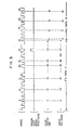
- Figure 3 shows the words received, a potentially valid data selection pulse, and the values of the control counter 50 and the buffer address counter during a single buffer load cycle.
- each positive pulse represents a black bar used on a label for data coding purposes and that each negative pulse represents a white bar (or space) on the same label.
- the value of the command counter and that of the address counter associated with the chosen buffer memory follow the number of data words received until the command counter reaches the first value, that is to say 42. If no potentially valid data selection pulse has been generated in the meantime, the two signals applied to the inputs of the OR gate 54 go to low level, which has the effect of blocking the AND gate 52 and preventing the application of other pulses to the counter 50.
- the address counter associated with the buffer memory 24 continues to be incremented at each transition so that the oldest data contained in the buffer memory can be replaced by the most recently received data .
- the flip-flop 66 When a potentially valid data selection pulse is finally generated, the flip-flop 66 is triggered and changes the output of the OR gate 54 to a high level. The command counter 50 then resumes counting the transitions, starting at the value 42. As long as the value 64 has not been reached, the data words received continue to be loaded into the buffer memory, the words stored most old ones being replaced by new words. When the value 64 is reached, the flip-flop 40 changes state and applies a signal to the AND gates associated with the buffer memory 26 which was previously inactive, these doors being turned on, while a signal is applied to the AND gates associated with the buffer memory 24, which is now completely filled, so as to block these latter doors.
- the address counter associated with the buffer memory 26 has been set to 1 either during startup, or after the last transfer of the content of the buffer memory to the processor 30.
- the command counter is also reset to 1 by the signal supplied by through its restore loop 60.
- the value of the command counter and that of the buffer address counter progress in an identical manner during the loading of the first 42 words of data into the buffer memory 26.
- the content of the buffer memory 34 is transferred to the processor 30 via the multiplexer 32.
- the storage control process relating to the buffer memory 26 is practically identical to that already described in the case of the buffer memory 24.
- the command counter 50 counts up to the value 42 and remains at this latter value unless the logic selection circuit 18 does not cause the flip-flop 66 to be triggered at a value between 1 and 42 to indicate that the buffer memory that is being loaded contains potentially valid data. If no potentially valid data signal is generated by the circuit 18 before the value 42 is reached, 42, the counter 50 remains at this value although the data words continue to be written in the buffer memory 26, the words the most recent ones replacing the oldest words. Counting resumes only when a pulse of potentially valid data causes the flip-flop 66 to engage.
- the advantage of this arrangement with two buffer memories is obvious.
- the processor 30 is only interrupted for the purpose of decoding when one of the buffer memories is completely filled and contains potentially valid data. No interruption occurs and a fully filled buffer does not contain potentially valid data or if a partially filled buffer contains such data.
- the data received is directed to another buffer memory when it has been found that the first contains potentially valid data, there is no loss of data even if the potentially valid data overlap or are nested.
Description
La présente invention concerne un circuit de commande de mémoire tampon tel que définit par la revendication 1 et, plus particulièrement, un tel circuit utilisable dans un analyseur optique.The present invention relates to a buffer memory control circuit as defined by
Un type bien connu d'analyseur qui permet de lire des étiquettes comportant des informations codées au moyen d'un code à barres tel que celui appelé dans la littérature anglo-saxonne "Universal Product Code" (UPC), balaie de façon répétée le produit sur lequel se trouve l'étiquette au moyen d'un faisceau de lumière cohérente lorsque le produit passe devant une fenêtre appropriée. La lumière qui est réfléchie à l'intérieur de cette fenêtre change d'intensité en fonction du pouvoir réfléchissant de la partie de la surface qui est frappée par le faisceau. Après avoir procédé à une conversion électrique de la lumière ainsi réfléchie, en utilisant un tube photo-multiplicateur ou une photodiode, on obtient une sinusoïde irrégulière présentant des crêtes positives et négatives. La longueur des parties positives et négatives du signal est proportionnelle à la largeur des barres claires et sombres que comporte l'étiquette lorsque cette dernière est effectivement frappée par le faisceau.A well-known type of analyzer which makes it possible to read labels comprising information coded by means of a bar code such as that called in the Anglo-Saxon literature "Universal Product Code" (UPC), repeatedly scans the product on which the label is located by means of a coherent beam of light when the product passes in front of an appropriate window. The light which is reflected inside this window changes intensity depending on the reflecting power of the part of the surface which is struck by the beam. After having carried out an electrical conversion of the light thus reflected, by using a photo-multiplier tube or a photodiode, an irregular sinusoid is obtained having positive and negative peaks. The length of the positive and negative parts of the signal is proportional to the width of the light and dark bars that the label contains when the latter is actually struck by the beam.
L'analyse d'une étiquette comportant des informations ainsi codées est rendue plus compliquée par le fait que la surface du produit qui se trouve à proximité de l'étiquette comporte généralement des symboles imprimés ou des dessins qui, lorsqu'ils sont balayés par le faisceau lumineux, provoquent la génération de signaux sinusoïdaux irréguliers. Il est donc nécessaire que l'analyseur puisse établir une distinction entre ces derniers signaux, qui sont sans intérêt du point de vue du décodage, et les signaux sinusoïdaux qui sont représentatifs des données codées que comporte l'étiquette.The analysis of a label containing information thus coded is made more complicated by the fact that the surface of the product which is located near the label generally comprises printed symbols or designs which, when scanned by the light beam, cause the generation of irregular sinusoidal signals. It is therefore necessary for the analyzer to be able to distinguish between these latter signals, which are irrelevant from the point of view of decoding, and the sinusoidal signals which are representative of the coded data which the label contains.
Afin de réduire au minimum la quantité de données brutes qu'il est nécessaire de décoder, les dispositifs de l'art antérieur comportent généralement des circuits de sélection ou de discrimination qui examinent les signaux engendrés par l'analyseur, un mot à la fois, au fur et à mesure que les données représentées par ces signaux sont chargées dans une mémoire tampon. Lorsqu'il résulte de cet examen que la mémoire tampon contient des données qui se rapportent vraisemblablement au contenu de l'étiquette, ces données sont transmises à un processeur, généralement au moyen d'une routine d'interruption, aux fins d'une analyse plus détaillée. La mémoire tampon ainsi débarrassée de son contenu peut alors recevoir de nouveaux signaux engendrés par l'analyseur. Les tests logiques effectués par les circuits logiques de sélection sont d'une nature grossière, c'est-à-dire moins rigoureux que ceux qui sont effectués par le processeur. Si l'on restreint la fonction de ces circuits logiques à l'exêcution de tests logiques grossiers, il devient possible de réduire le coût du matériel requis aux fins de mise en oeuvre de cette sélection. Chose plus importante, il y a moins de chances, dès lors que l'on procède à des tests grossiers, pour que des données se rapportant effectivement au contenu d'une étiquette ne soient pas détectées.In order to minimize the amount of raw data that it is necessary to decode, the devices of the prior art generally include selection or discrimination circuits which examine the signals generated by the analyzer, one word at a time, as the data represented by these signals are loaded into a buffer memory. When it results from this examination that the buffer contains data which probably relate to the content of the label, this data is transmitted to a processor, generally by means of an interrupt routine, for the purposes of analysis. more detailed. The buffer memory thus freed of its content can then receive new signals generated by the analyzer. The logic tests carried out by the logic selection circuits are of a crude nature, that is to say less rigorous than those carried out by the processor. If the function of these logic circuits is limited to the execution of rough logic tests, it becomes possible to reduce the cost of the material required for the purposes of implementing this selection. More importantly, there is less chance that when coarse testing is done, data that actually relates to the content of a label will not be detected.
Toutefois, le processus de sélection étant d'une nature grossière, il peut arriver que des données soient identifiées à tort comme se rapportant au contenu d'une étiquette, ou qu'un conflit existe à cet égard entre différents ensembles de données.However, the selection process being of a crude nature, it may happen that data is wrongly identified as relating to the content of a label, or that a conflict exists in this respect between different sets of data.
Si l'analyseur ne doit être employé que pour lire un unique type de données codées sur les étiquettes, il est possible de réaliser des circuits de sélection capables de résoudre ce dernier type de problème. Il existe d'ailleurs différents types de codes à barre actuellement utilisés ou dont l'on envisage l'emploi, y compris différentes versions du code UPC et du code appelé dans la littérature anglo-saxonne "European Article Number" (EAN).If the analyzer should only be used to read a single type of data coded on the labels, it is possible to make selection circuits capable of solving the latter type of problem. There are, moreover, different types of bar codes currently in use or which are envisaged for use, including different versions of the UPC code and of the code called in the Anglo-Saxon literature "European Article Number" (EAN).
Bien qu'il soit théoriquement possible de réaliser différents circuits de sélection dont chacun serait consacré à l'exécution de tests afférents à un unique code, cette solution serait d'un prix prohibitif.Although it is theoretically possible to carry out different selection circuits, each of which would be devoted to the execution of tests relating to a single code, this solution would be prohibitively expensive.
Une autre solution consisterait à effecteur un minimum de tests grossiers ou à n'effectuer aucun test grossier, la quasi totalité des données brutes fournies par l'analyseur étant alors transmise à un processeur aux fins d'une analyse rigoureuse. L'inconvénient de cette solution réside dans le fait qu'elle exigerait qu'une partie très importante de la totalité du temps de fonctionnement du processeur soit consacrée à trier des quantités considérables de données brutes engendrées pendant le fonctionnement de l'analyseur de manière à séparer les données relativement peu nombreuses qui se rapportent effectivement au contenu d'une étiquette des autres données, lesquelles sont dépourvues de signification. Etant donné que le processeur est généralement utilisé à des fins de supervision ou de calcul, il en résulterait nécessairement une dégradation du temps de réponse du système. Pour obtenir un temps de réponse acceptable, il faudrait vraisemblablement utiliser un processeur coûteux et plus puissant.Another solution would be to carry out a minimum of coarse tests or not to carry out any coarse test, almost all of the raw data supplied by the analyzer then being transmitted to a processor for the purpose of a rigorous analysis. The disadvantage of this solution is that it would require a very large part of the total operating time of the processor to be spent sorting through considerable amounts of raw data generated during the operation of the analyzer so as to separate relatively few data that actually relate to the content of a label from other data, which is meaningless. Since the processor is generally used for supervision or calculation purposes, this would necessarily result in a degradation of the system response time. To obtain an acceptable response time, it would probably be necessary to use an expensive and more powerful processor.
Enfin il est également commun, d'après le document US-A-3 868 636 d'utiliser dans un dispositif de reconnaissance de caractères, deux registres à décalage destinés a emmagasiner les données résultant de la partition du caractère balayé.Finally, it is also common, according to document US-A-3 868 636 to use in a character recognition device, two shift registers intended to store the data resulting from the partition of the scanned character.
La présente invention concerne un circuit de commande de mémoire tampon qui permet de sauvegarder, en vue de leur transfert ultérieur à un processeur, toutes les données identifiées par des circuits logiques de sélection comme étant des données potentiellement valides, c-est-à-dire susceptibles de se rapporter au contenu d'une étiquette, tout en rejetant la plupart des autres données brutes engendrées par l'analyseur. Ledit circuit permet également de diminuer le temps que le processeur doit consacrer à une analyse plus détaillée et au décodage des données.The present invention relates to a buffer memory control circuit which makes it possible to save, with a view to their subsequent transfer to a processor, all the data identified by logical selection circuits as being potentially valid data, that is to say capable of relating to the content of a label, while rejecting most of the other raw data generated by the 'analyzer. Said circuit also makes it possible to reduce the time that the processor must devote to a more detailed analysis and to the decoding of the data.
Un circuit de commande réalisé conformément à la présente invention est utilisé avec plusieurs dispositifs d'emmagasinage de données, l'un desquels est choisi toujours actif, c'est-à-dire mis en état d'emmagasiner des éléments de données reçus en série. Le circuit de commande comprend des moyens permettant d'examiner ces éléments et d'engendrer un signal dit de "données potentiellement valides" (DPV) lorsqu'un permier nombre desdits éléments satisfait à des critères prédéterminés; il comprend également des moyens permettant de compter les éléments de données jusqu'à ce qu'une valeur correspondant à ce premier nombre soit atteinte et de maintenir cette valeur à moins que ou jusqu'à ce qu'un signal DPV soit engendré. Un dispositif de commutation permet, lorsqu'un second nombre d'éléments de données supérieur audit premier nombre est atteint, de mettre un dispositif d'emmagasinage de données, précédemment rendu inactif, en état de recevoir des éléments de données ultérieurs. Les données contenues dans le dispositif d'emmagasinage précédemment rendus actif sont transférées à un processeur aux fins d'une analyse détaillée.A control circuit produced in accordance with the present invention is used with several data storage devices, one of which is chosen to be always active, that is to say set to store data elements received in series . The control circuit comprises means making it possible to examine these elements and to generate a so-called "potentially valid data" (DPV) signal when a first number of said elements satisfies predetermined criteria; it also includes means for counting the data elements until a value corresponding to this first number is reached and for maintaining this value unless or until a DPV signal is generated. A switching device allows, when a second number of data elements greater than said first number is reached, to put a data storage device, previously rendered inactive, in a state to receive subsequent data elements. The data in the storage device previously made active is transferred to a processor for detailed analysis.
D'autres objets, caractéristiques et avantages de la présente invention ressortiront mieux de l'exposé qui suit, fait en référence aux dessins annexés à ce texte, qui représentent un mode de réalisation préféré de celle-ci.Other objects, characteristics and advantages of the present invention will emerge more clearly from the following description, made with reference to the drawings appended to this text, which represent a preferred embodiment thereof.
- La Figure 1 est un schéma synoptique d'un dispositif d'analyse comprenant le présente invention.Figure 1 is a block diagram of an analysis device comprising the present invention.
- La Figure 2 est un schéma synoptique plus détaillé des éléments d'un circuit de commande de mémoire tampon réalisé conformément à la présente invention.Figure 2 is a more detailed block diagram of the elements of a buffer control circuit constructed in accordance with the present invention.
- La Figure 3 représente schématiquement les signaux et les valeurs engendrés lors de la détection d'un unique ensemble de données potentiellement valides.Figure 3 schematically represents the signals and values generated during the detection of a single set of potentially valid data.
On a schématiquement représenté sur la Figure 1 un dispositif de lecture d'étiquettes dans lequel la présente invention peut être utilisée et qui comprend un analyseur 10. Ce dernier, qui peut être d'un type classique, comprend de préférence un laser, des éléments de déviation de faisceau qui permettent d'engendrer une configuration de balayage au moyen du faisceau laser, des circuits de conversion permettant d'obtenir un signal électrique qui varie en fonction de l'intensité de la lumière réfléchie, ainsi que des circuits de seuil ou d'autres circuits de mise en forme d'impulsions qui permettent d'obtenir un train d'impulsions carrées à partir d'un signal sinusoïdal irrégulier.Schematically shown in Figure 1 a label reading device in which the present invention can be used and which comprises an
Ce train d'impulsions est appliqué à la fois à un détecteur de transitions 12 et à un compteur 14. La fonction du détecteur 12 est de fournir un signal chronologique coïncidant avec l'apparition du front avant de chaque impulsion positive et de chaque impulsion négative. Le compteur 14 engendre un mot binaire dont la valeur est fonction de la largeur de chaque impulsion. Ce compteur se compose de préférence d'un compteur binaire excité par une horloge HF. L'excitation du compteur coïncide avec l'apparition du front avant de chaque impulsion et prend fin lors de l'apparition du front arrière. La valeur du signal de sortie du compteur est directement proportionnelle à la largeur des impulsions.This train of pulses is applied both to a
Les signaux ou les mots binaires obtenus à la sortie du compteur 14 sont appliqués en parallèle par l'intermédiaire d'un câble 16 à un circuit logique de sélection 18. La fonction de ce dernier est d'examiner les données qu'il reçoit et de fournir un signal de données potentiellement valides (DPV) chaque fois qu'un nombre prédéterminé de mots successifs satisfait à des tests logiques grossiers. Des circuits de ce type sont décrits notamment dans les documents US-A-3 909 787 et 4 086 477. Le signal DPV engendré par le circuit 18 est de préférence a bits multiples et indique non seulement que des données potentiallement valides ont été trouvées, mais aussi la direction dans laquelle l'étiquette a fait l'objet d'un balayage. Ce signal est ajouté à l'un des mots de données transmis sur le câble 16. Etant donné qu'un intervalle de temps fini est nécessaire pour mener à bonne fin les tests logiques grossiers effectués par le circuit 18, ledit signal n'est pas ajouté au denier mot du bloc de données potentiellement valides, mais est séparé de celui-ci par un ou plusieurs mots de données. Par exemple, si un tel bloc est constitué par 20 mots, ledit signal est ajouté au second mot qui fait suite à ce bloc, c'est-à-dire au 22ème mot. La valeur de ce décalage est fixée lors de la conception du dispositif.The signals or binary words obtained at the output of the
Le mot ainsi obtenu, qui se compose des sorties combinées du compteur 14 et du circuit logique 18, est appliqué à une paire de circuits de commande de mémoire tampon 20 et 22 qui seront décrits plus loin. D'une façon générale, la fonction de chacun de ces circuits est de commander l'emmagasinage des mots de données reçus par l'intermédiaire du câble 16 dans l'une ou l'autre de deux mémoires tampons, qui sont de préférence identiques, 24 et 26, est emmagasinage étant effectué sous le contrôle d'un circuit de sélection de mémoire tampon 28. Ce dernier, qui sera décrit plus loin, fonctionne lui- même sous le contrôle des signaux d'entrée qu'il reçoit du circuit 18 et du détecteur 12.The word thus obtained, which consists of the combined outputs of the
Le circuit de sélection 28 engendre également un signal de sortie qui est appliqué à un processeur 30 lorsqu'il s'avère que l'une des mémoires tampons est complètement rempole et contient des données potentiellement valides. Afin d'éviter toute parte de données, le circuit 28, tout en transmettant ledit signal au processeur 30, provoque l'emmagasinage des données que l'on est en train de recevoir dans la mémoire tampon qui était précédemment inactive. En réponse, le processeur 30 commande un circuit de multiplexage 32 de manière à assurer le transfort des données contenues dans la mémoire tampon compètement remplie.The
En résumé, les mots de données reçus sont dirigés par l'intermédiaire de l'un des circuits de commande 20, 22 vers une mémoire tampon active tout en étant examinés par le circuit de sélection 18. Si la mémoire tampon active est remplie, les données les plus anciennes sont remplacées par les données nouvellement reçues. Lorsque le circuit logique 28 constate que la mémoire tampon active est remplie et contient un bloc de données potentiellement valides, les mots de données reçus sont chargés dans la mémoire tampon qui était précédemment inactive et le processeur 30 est informé en conséquence, de telle sorte qu'il puisse alors commencer à transférer les données depuis la mémoire tampon complètement chargée par l'intermédiaire du multiplexeur 32. Le processeur 30 effectue alors une analyse plus rigoureuse des données afin de déterminer de façon définitive si ces dernières se rapportent effectivement au contenu d'une étiquette.In summary, the data words received are directed via one of the
La Figure 2 représente de façon plus détaillée les circuits de commande de mémoire tampon et le circuit de sélection de mémoire tampon 28. Cette figure comprend essentiellement tous les éléments contenus à l'intérieur du cadre pointillé 34 de la Figure 1. Les signaux dont l'origine se situe à l'extérieur de ce cadre sont identifiés au moyen d'une référence aux composants dont ils émanent.Figure 2 shows in more detail the buffer control circuits and the
Dans une réalisation préférée de l'invention, les mémoires tampons 24 et 26 sont du type à accès sélectif ou directement adressable et comportent plusieurs positions de mémoire dont chacune peut être adressée séparément et contenir un mot de plusieurs bits. Le nombre de positions de mémoire de chaque mémoire tampon est supérieur au nombre de mots requis pout constituer un bloc de données potentiellement valides. Le circuit de commande 20 afférent à la mémoire tampon 24 comprend un compteur d'adresse 36 dont la valeur maximale correspond au nombre de positions de mémoire que comporte la mémoire tampon 24. Le compteur 36 est excité au moyen de la sortie d'une porte ET 38 à deux entrées, l'une desquelles reçoit la sortie d'un dispositif bistable tel qu'un flip-flop 40, qui change d'état chaque fois qu'une impulsion est appliquée à son entrée d'horloge (C), l'autre entrée de la porte ET 38 recevant la sortie du détecteur de transitions 12. Lorsque le flip-flop 40 est restauré, chaque transition du signal fourni par l'analyseur 10 rend la porte ET 38 passante. De ce fait, la valeur du compteur 36 est incrémentée d'une unité de façon à désigner une nouvelle position d'emmagasinage de la mémoire tampon 24. La sortie inversée du flip-flop 40 est également appliquée à l'une des entrées de chacune des portes ET que comporte un ensemble 42, la seconde entrée de chacune desdites portes recevant la sortie transmise par l'intermédiaire de l'un des conducteurs contenus dans le câble d'entrée 16. L'ensemble de portes ET 42 transmet n'importe quel mot fourni par le compteur 14 et par le circuit logique 18 tant que le flip-flop 40 se trouve dans son état restauré. La position de mémoire vers laquelle le mot est dirigé est fonction de la sortie actuelle du compteur 36.In a preferred embodiment of the invention, the
Le circuit de commande associé à la seconde mémoire tampon 26 est pratiquement identique au circuit de commande déjà décrit. De façon plus précise, le circuit de commande de la mémoire tampon 26 comprend un compteur d'adresses 44 à autorestauration qui est excité par la sortie d'une porte ET 46 à deux entrées, ainsi qu'un ensemble 48 de portes ET dont chacune est connectée à un conducteur différent contenu dans le câble 16 et possède une connexion commune avec le flip-flop 40.The control circuit associated with the
La seule différence entre les circuits 20 et 22 réside dans le fait qu'ils sont commandés par les sorties complémentaires du flip-flop 40. Lorsque ce dernier se trouve dans son état restauré, la porte ET 38 et les portes ET que comporte l'ensemble 42 sont rendues passantes de telle sorte que les données puissent être emmagasinées dans la mémoire tampon 24 dans des positions adressées de façon séquentielle. Pendant ce temps, les portes ET de l'ensemble 48 et la porte ET 46 sont bloquées par un signal de niveau bas émanant du flip-flop 40 de telle sorte que la mémoire tampon 26 ne puisse pas recevoir les données. Lorsque le flip-flop 40 se trouve dans son état opposé (enclenché), les portes ET associées à la mémoire tampon 26 sont rendues passantes et de ce fait les données reçues peuvent être emmagasinées dans des positions de cette mémoire tampon qui sont adressées de façon séquentielle. Dans le même temps, les portes ET associées à la mémoire tampon 24 sont bloquées par un signal de niveau bas obtenu à la sortie inversée du flip-flop 40.The only difference between
Le flip-flop 40 est l'un des composants du circuit de sélection de mémoire tampon 28. L'état de ce flip-flop est déterminé par un compteur de commande 50, qui est de préfé- ren.çe un compteur binaire à auto-restauration capable d'atteindre une valeur maximale correspondant au nombre de positions de mémoire que comporte chacune des mémoires tampons 24 et 26. Le compteur 50 est excité au moyen d'impulsions fournies par une porte ET 52 à deux entrées, l'une desquelles reçoit une impulsion chaque fois que le détecteur de transition 12 détecte le front avant d'une impulsion positive ou d'une impulsion négative émanant de l'analyseur, la seconde entrée de la porte ET 52 recevant, dans des conditions qui seront précisées ultérieurement, la sortie d'une porte OU 54 faisant partie du circuit de sélection de mémoire tampon 28.The flip-
La sortie du compteur 50 est transmise à deux circuits logiques 56 et 58. Ces derniers peuvent se composer d'ensembles de portes ET connectées à des étages particuliers du compteur 50 de telle sorte que des signaux logiques de sortie positifs ne soient engendrés que lorsqu'une première valeur et une seconde valeur du compteur sont respectivement atteintes. Le circuit logique 56 a pour fonction de reconnaître l'instant où le compteur 50 a atteint ladite première valeur, qui correspond au nombre de mots constituant la totalité d'un bloc de données potentiellement valides plus le nombre de mots représentant le retard du signal dit de données potentiellement valides (DPV) et séparant la génération de celui-di du dernier mot du bloc. Par example, si un tel bloc nécessitait l'emmagasinage de 40 mots dans l'une des mémoires tampons 24 et 26 et si le retard dudit signal correspondait à deux unités de comptage ou à deux mots, la logique 56 serait conçue de manière à détecter l'instant où la valeur quarante-deux serait atteinte.The output of the
La fonction du circuit logique 58 est de détecter une seconde valeur, correspondant à la capacité maximale d'emmagasinage de mots que présentent les mémoires tampons 24 et 26. Par exemple, si chacune de ces mémoires avait une capacité de 64 mots de plusieurs bits, le circuit logique 58 fournirait une sortie positive lorsque la valeur 64 serait atteinte. Une boucle de restauration 60 permet de remettre le compteur 50 à une valeur initiale (de préférence zéro) une fois que ladite seconde valeur a été détectée. La sortie du circuit logique 58 est appliquée à l'entrée d'horloge (C) du flip-flop 40, aux entrées d'enclenchement (S) respectives de deux flip-flop 62 et 64, et à l'entrée de restauration (R) d'un autre flip-flop 66. Ainsi qu'on le verra plus loin, le compteur 50 n'atteint la seconde valeur que lorsque l'une des mémoires tampon 24 et 26 est complètement remplie et contient un bloc de données potentiellement valides. Le flip-flop 62 répond à la détection de ladite seconde valeur en transmettant un signal de demande d'interruption au processeur 30 afin de provoquer le transfert des données contenues dans la mémoire tampon au processeur par l'intermédiaire du multiplexeur 32. Le flip-flop 62 est restauré par le processeur 30 lorsque ce transfert a été effectué.The function of
Le flip-flop 64 est restauré par la sortie engendrée par le circuit logique 56 lorsque la première valeur est atteinte par le compteur de commande 50, et est enclenché par la sortie engendrée par le circuit logique 58 lorsque la seconde valeur est atteinte. De ce fait, le flip-flop 64 fournit un signal de niveau haut chaque fois que la valeur de la sortie du compteur 50 varie entre l'unité et ladite première valeur. Si l'on utilise les valeurs données plus haut comme exemples, le flip-flop 64 engendre un signal de niveau haut à toutes les valeurs de 1 à 42, et un signal de niveau bas à toutes les valeurs de 43 à 64. La sortie du flip-flop 64 est appliquée à l'une des entrées d'une porte OU 54.The flip-
Le flip-flop 66 est enclenché chaque fois que le circuit logique de sélection 18 détecte un bloc de données potentiellement valides et est restauré lorsque la seconde valeur est atteinte. L'intervalle de temps pendant lequel le flip-flop 66 est enclenché ou restauré est indéfini et peut varier considérablement d'un cycle de fonctionnement à l'autre, en fonction uniquement de l'instant où le bloc est détecté.The flip-
D'une façon générale, les composante logiques associés au compteur 50 permettent à celui-ci de compter jusqu'à ce que la première valeur soit atteinte, si aucun bloc de données potentiellement valides n'a été obtenu. Le compteur est maintenu à cette première valeur pendant que les données correspondant aux signaux que l'on est en train de recevoir continuent à être chargées dans la mémoire tampon active. Lorsque le circuit logique 18 détecte un tel bloc, le compteur 50 est incrémenté d'une unité par mot reçu jusqu'à ce que la seconde valeur ait été atteinte, le flip-flop 40 changeant alors d'état pour diriger les mots ultérieurement reçus vers la mémoire tampon qui était précédemment inactive. Le flip-flop 62 est enclenché de manière à ce qu'un signal soit transmis au processeur 30 afin que les données soient transférées à ce dernier, depuis la mémoire tampon complètement remplie, par l'intermédiaire du multiplexeur 32.Generally, the logic components associated with
Pour les besoins de la description du mode de fonctionnement du circuit, on suppose l'existence de certaines conditions initiales. Tout d'abord, on suppose que la capacité maximale de chacune des mémoires tampons 24 et 26 est de 64 mots, ce qui correspond à le seconde valeur, ou valeur maximum, que le compteur de commande 50 peut atteindre. On suppose également qu'un bloc de données potentiellement valides se compose de quarante mots et que le signal DPV est séparé de ce bloc par deux mots, la première valeur étant donc égale à 42. Le flip-flop 40 est initialement restauré de telle sorte que la porte ET 38 et les portes ET de l'ensemble 42 soient partiellement passantes. Le compteur d'adresses 36 est initialement mis à 1 afin d'adresser la première position de mémoire que comporte la mémoire tampon 24.For the purposes of describing the operating mode of the circuit, we assume the existence of certain initial conditions. First of all, it is assumed that the maximum capacity of each of the
Lorsque le circuit est mis sous tension, le détecteur de transitions 12 cherche de façon continue à déterminer l'apparition d'une transition. Rien ne se passe tant qu'une transition n'a pas été détectée. Dans le cas contraire, le mot reçu est transmis par l'intermédiaire de l'ensemble 42 de portes ET à la première position de mémoire de la mémoire tampon 26. La transition ainsi détectée est également transmise par l'intermédiaire de la porte ET 38 au compteur d'adresses 36 de manière à incré- menter d'une unité la valeur de l'adresse.When the circuit is energized, the
Si la valeur du compteur de commande 50 est inférieure à 42 cette valeur est incrémentée d'une unité et le processus recommence. Après la première transition, les compteurs 50 et 36 se trouvent à la valeur 1 et un mot est emmagasiné dans la mémoire tampon 24.If the value of the
Ce processus est répété a chaque transition du signal reçu jusqu'à ce que l'on ait déterminé que la valeur du compteur 50 est au moins égale à 42. On détermine alors si cette valeur est supérieure ou égale à 42, mais inférieure à 64. Si la valeur est comprise entre ces limites, on procède à une vérification pour déterminer si un bloc de données potentiellement valides a été trouvé. Si tel n'est pas le cas, le processus recommence. Si, au contraire, un tel bloc a été trouvé pendant le cycle de comptage en cours (c'est-à-dire de 1 à la valeur actuelle), la valeur du compteur 50 est incrémentée avant que le processus ne recommence.This process is repeated at each transition of the received signal until it has been determined that the value of the
Les étapes qui viennent d'être décrites sont répétées jusqu'à ce que la vérification de la valeur du compteur 50 indique que celle-ci est égale à 64, ce qui indique que l'une des mémoires tampons est complètement remplie et contient au moins quelques mots constituant des données potentiellement valides. Le compteur 50 est alors remis à 1 par l'intermédiaire de la boucle de restauration 60. Le flip-flop 40 est enclenché de manière à rendre actif le circuit de commande 22 associé à la mémoire tampon 26. Dans le même temps, le flip-flop 62 est enclenché et transmet au processeur 30 un signal qui provoque le transfert au processeur des données contenues dans la mémoire tampon 24.The steps which have just been described are repeated until the verification of the value of the
Le cycle de chargement de mémoire tampon est répété de la façon décrite, que la mémoire tampon active soit la mémoire tampon 24 ou 26. On notera cependant que, bien que le compteur de commande 50 s'arrête à la valeur 42 ou soit maintenu à cette valeur à moins qu'une impulsion de sélection de données potentiellement valides n'ait été engendrée avant que le compteur 50 ait atteint cette valeur, les mots de données continuent à être écrits dans la mémoire tampon 26 de façon cyclique, les données les plus récentes étant écrites dans la position de mémoire qui contient les données les plus anciennes. Le compteur 50 ne peut dépasser la valeur 42 que lorsqu'une impulsion de sélection de données potentiallement valides est engendrée pendant le cycle de comptage en cours.The buffer loading cycle is repeated as described, whether the active buffer is
On a supposé dans un but de clarté que toutes les opérations étaient effectuées de façon séquentielle. Cette supposition serait vraie si l'invention devait être mise en oeuvre en programmant un processeur à usage multiples, ce qui se trouve effectivement dans le domaine d'application de l'invention. Toutefois, si l'invention est mise en oeuvre sous la forme d'éléments matériels, les opérations peuvent être effectuées simultanément et non plus séquen- tiellement. Par exemple, les vérifications effectuées aux blocs 74 et 78 seraient séquentielles dans un système logiciel, mais simultanées dans un système composé d'éléments matériels.It has been assumed for the sake of clarity that all operations are carried out sequentially. This assumption would be true if the invention were to be implemented by programming a multi-use processor, which is effectively within the scope of the invention. However, if the invention is implemented in the form of material elements, the operations can be carried out simultaneously and no longer sequentially. For example, the checks performed at blocks 74 and 78 would be sequential in a software system, but simultaneous in a system composed of hardware elements.
La Figure 3 représente les mots reçus, une impulsion de sélection de données potentiellement valides et les valeurs du compteur de commande 50 et du compteur d'adresses de mémoire tampon lors d'un unique cycle de chargement de mémoire tampon. Sur la Figure 3, on peut supposer que chaque impulsion positive représente une barre noire utilisée sur une étiquette aux fins du codage de données et que chaque impulsion négative représente une barre blanche (ou un espace) sur la même étiquette. La valeur du compteur de commande et celle du compteur d'adresses associé à la mémoire tampon choisie suivent le nombre de mots de données reçus jusqu'à ce que le compteur de commande atteigne la première valeur, c'est-à-dire 42. Si aucune impulsion de sélection de données potentiellement valides n'a été engendrée entre-temps, les deux signaux appliqués aux entrées de la porte OU 54 passent au niveau bas, ce qui a pour effet de bloquer la porte ET 52 et d'empêcher l'application d'autres impulsions au compteur 50. Le compteur d'adresses associé à la mémoire tampon 24 continue à être incrémenté à chaque transition afin que les données les plus anciennes contenues dans la mémoire tampon puissent être remplacées par les données les plus récemment reçues.Figure 3 shows the words received, a potentially valid data selection pulse, and the values of the
Lorsqu'une impulsion de sélection de données potentiellement valides est finalement engendrée, le flip-flop 66 est enclenché et fait passer la sortie de la porte OU 54 à un niveau haut. Le compteur de commande 50 reprend alors le comptage des transitions, en commençant à la valeur 42. Tant que la valeur 64 n'a pas été atteinte, les mots de données reçus continuent à être chargés dans la mémoire tampon, les mots emmagasinés les plus anciens étant remplacés par de nouveaux mots. Lorsque la valeur 64 est atteinte, le flip-flop 40 change d'état et applique un signal aux portes ET associées à la mémoire tampon 26 qui était précédemment inactive, ces portes étant rendues passantes, cependant qu'un signal est appliqué aux portes ET associées à la mémoire tampon 24, qui se trouve à présent complètement remplie, de manière à bloquer ces dernières portes. Le compteur d'adresses associé à la mémoire tampon 26 a été mis à 1 soit pendant le démarrage, soit après le dernier transfert du contenu de la mémoire tampon au processeur 30. Le compteur de commande est également remis à 1 par le signal fourni par l'intermédiaire de sa boucle de restauration 60. De ce fait, la valeur du compteur de commande et celle du compteur d'adresses de mémoire tampon progressent de façon identique pendant le chargement des 42 premiers mots de données dans la mémoire tampon 26. Pendant que ce chargement est effectué, le contenu de la mémoire tampon 34 est transféré au processeur 30 par l'intermédiaire du multiplexeur 32.When a potentially valid data selection pulse is finally generated, the flip-
Le processus de commande d'emmagasinage afférent à la mémoire tampon 26 est pratiquement identique à celui déjà décrit dans le cas de la mémoire tampon 24. Le compteur de commande 50 compte jusqu'à la valeur 42 et reste à cette dernière valeur à moins que le circuit logique de sélection 18 ne provoque l'enclenchement du flip-flop 66 à une valeur comprise entre 1 et 42 pour indiquer que la mémoire tampon que l'on est en train de charger contient des données potentiellement valides. Si aucun signal de données potentiellement valides n'est engendré par le circuit 18 avant que la valeur 42 soit atteinte, 42, le compteur 50 reste à cette valeur bien que les mots de données continuent à être écrits dans la mémoire tampon 26, les mots les plus récents remplaçant les mots les plus anciens. Le comptage reprend seulement lorsqu'une impulsion de données potentiellement valides provoque l'enclenchement du flip-flop 66.The storage control process relating to the
L'avantage que présente cet agencement à deux mémoires tampon est évident. Le processeur 30 ne fait l'objet d'une interruption aux fins d'un décodage que lorsque l'une des mémoires tampon est complètement remplie et contient des données potentiellement valides. Aucune interruption ne se produit et une mémoire tampon complètement remplie ne contient pas de données potentiellement valides ou si une mémoire tampon partiellement remplie contient de telles données. D'autre part, comme les données reçues sont dirigées vers une autre mémoire tampon lorsqu'on a constaté que la première contenait des donnée potentiellement valides, il ne se produit aucune perte de données même si les données potentiellement valides se chevauchent ou sont emboîtées.The advantage of this arrangement with two buffer memories is obvious. The
Bien que l'on ait décrit dans ce qui précède et représenté sur les dessins les caractéristiques essentielles de l'invention appliquées à un mode de réalisation préféré de celle-ci, il est évident que l'homme de l'art peut y apporter toutes modifications de forme ou de détail qu'il juge utiles, sans pour autant sortir du cadre de ladite invention.Although the essential characteristics of the invention applied to a preferred embodiment of the invention have been described in the foregoing and represented in the drawings, it is obvious that a person skilled in the art can provide all of them. modifications of form or detail which he judges useful, without departing from the scope of said invention.
Claims (8)
Applications Claiming Priority (2)
| Application Number | Priority Date | Filing Date | Title |
|---|---|---|---|
| US98461 | 1979-11-29 | ||
| US06/098,461 US4344152A (en) | 1979-11-29 | 1979-11-29 | Buffer memory control circuit for label scanning system |
Publications (2)
| Publication Number | Publication Date |
|---|---|
| EP0029923A1 EP0029923A1 (en) | 1981-06-10 |
| EP0029923B1 true EP0029923B1 (en) | 1985-02-06 |
Family
ID=22269373
Family Applications (1)
| Application Number | Title | Priority Date | Filing Date |
|---|---|---|---|
| EP80106693A Expired EP0029923B1 (en) | 1979-11-29 | 1980-10-31 | Buffer memory control circuit |
Country Status (5)
| Country | Link |
|---|---|
| US (1) | US4344152A (en) |
| EP (1) | EP0029923B1 (en) |
| JP (1) | JPS5679371A (en) |
| CA (1) | CA1148259A (en) |
| DE (1) | DE3070126D1 (en) |
Families Citing this family (8)
| Publication number | Priority date | Publication date | Assignee | Title |
|---|---|---|---|---|
| US4500880A (en) * | 1981-07-06 | 1985-02-19 | Motorola, Inc. | Real time, computer-driven retail pricing display system |
| JPH02500062A (en) * | 1986-09-18 | 1990-01-11 | ハドソン‐アレン リミテッド | Digital processing of sensor signals for reading binary storage media |
| JPS63135827U (en) * | 1987-02-26 | 1988-09-06 | ||
| JP3313362B2 (en) * | 1990-10-04 | 2002-08-12 | 日本電気株式会社 | Memory address generator for voice processing unit |
| WO1993003455A1 (en) * | 1991-08-02 | 1993-02-18 | Intermec Corporation | Method and apparatus for scanning symbols |
| DE69232493T2 (en) * | 1991-10-21 | 2003-01-09 | Canon Kk | Method and device for character recognition |
| AU3497497A (en) | 1996-06-21 | 1998-01-07 | Norand Corporation | Too long code reader performing coded image decoding |
| US20040064455A1 (en) * | 2002-09-26 | 2004-04-01 | Eastman Kodak Company | Software-floating palette for annotation of images that are viewable in a variety of organizational structures |
Family Cites Families (9)
| Publication number | Priority date | Publication date | Assignee | Title |
|---|---|---|---|---|
| US3752958A (en) * | 1971-12-07 | 1973-08-14 | Ncr | Field detection logic |
| US3868634A (en) * | 1972-11-03 | 1975-02-25 | Scanner | Reading of contrasting data by means of continuously attempting to decode read signals |
| US3868636A (en) * | 1973-06-18 | 1975-02-25 | Isotec Inc | Optical character reader having feature recognition capability |
| US3909787A (en) * | 1974-07-01 | 1975-09-30 | Ibm | Candidate selection processor |
| JPS586982B2 (en) * | 1976-08-18 | 1983-02-07 | 株式会社デンソー | Barcode reading method and device |
| US4086477A (en) * | 1977-06-27 | 1978-04-25 | International Business Machines Corporation | Decoding method and circuit |
| US4125765A (en) * | 1977-06-27 | 1978-11-14 | International Business Machines Corporation | Label find method and circuit |
| US4162035A (en) * | 1977-09-23 | 1979-07-24 | General Signal Corporation | High resolution optical position code detector for information recorded on record carrier partially in humanly intelligible form |
| US4298954A (en) * | 1979-04-30 | 1981-11-03 | International Business Machines Corporation | Alternating data buffers when one buffer is empty and another buffer is variably full of data |
-
1979
- 1979-11-29 US US06/098,461 patent/US4344152A/en not_active Expired - Lifetime
-
1980
- 1980-09-12 JP JP12619380A patent/JPS5679371A/en active Granted
- 1980-09-26 CA CA000361883A patent/CA1148259A/en not_active Expired
- 1980-10-31 EP EP80106693A patent/EP0029923B1/en not_active Expired
- 1980-10-31 DE DE8080106693T patent/DE3070126D1/en not_active Expired
Also Published As
| Publication number | Publication date |
|---|---|
| US4344152A (en) | 1982-08-10 |
| JPS5679371A (en) | 1981-06-29 |
| EP0029923A1 (en) | 1981-06-10 |
| CA1148259A (en) | 1983-06-14 |
| JPS6113636B2 (en) | 1986-04-14 |
| DE3070126D1 (en) | 1985-03-21 |
Similar Documents
| Publication | Publication Date | Title |
|---|---|---|
| EP0023271B1 (en) | Microprocessor-controlled data-input keyboard with variable-impedance keys | |
| CA2191787C (en) | Remote label reading method and station and label used in said method | |
| EP0108655B1 (en) | System for the detection and correction of transmission errors in a binary message using an error detecting and correcting interleaved reed-solomon cyclic code | |
| EP0104293B1 (en) | Device for loading and reading different chains of bistable circuits in a data processing system | |
| EP0029923B1 (en) | Buffer memory control circuit | |
| BE897586A (en) | PARALLEL CIRCUIT FOR CYCLIC REDUNDANCY CONTROL | |
| FR2627004A1 (en) | MEMORY DEVICE HAVING THE FUNCTION OF DETECTING AND CORRECTING AN ERROR IN STORED INFORMATION | |
| FR2635207A1 (en) | Method and device for processing an analog electrical signal with a view to obtaining a binary signal whose parameters can be analysed which is representative of its significant component | |
| EP0022004A1 (en) | Method of controlling comparison between reference logical entities and logical entities of a file | |
| EP1080431A1 (en) | Ques | |
| CH629319A5 (en) | DATA PROCESSING FACILITY. | |
| WO2010070594A2 (en) | Matrix sensor | |
| FR2511528A1 (en) | OPTICAL MULTIPLEXING ENCODER DEVICE | |
| FR2631724A1 (en) | COLONY COUNTING APPARATUS | |
| FR2672709A1 (en) | Command status machine | |
| BE897587A (en) | PARALLEL CIRCUIT FOR CYCLIC REDUNDANCY CONTROL | |
| EP0517335A1 (en) | Frequency-divider circuit | |
| FR2473753A1 (en) | DEVICE FOR PROVIDING CORRECTED DATA GROUPS TO A DESTINATION CIRCUIT | |
| EP0400520B1 (en) | Receiving signal drop-out detecting device for digital signal receiver | |
| EP0633457B1 (en) | Photosensitive element and apparatus for the detection of light pulses | |
| EP0004520A1 (en) | Keyboard with an array of light beam splitters | |
| EP0833346B1 (en) | Serial access memory with secured writing | |
| EP0367345A1 (en) | Logic analyser with double triggering | |
| EP0248712A1 (en) | Security keyboard unit, in particular for the composition of a confidential code | |
| EP0112429A1 (en) | System for the transmission of data by repetitive sequences |
Legal Events
| Date | Code | Title | Description |
|---|---|---|---|
| PUAI | Public reference made under article 153(3) epc to a published international application that has entered the european phase |
Free format text: ORIGINAL CODE: 0009012 |
|
| AK | Designated contracting states |
Designated state(s): CH DE FR GB IT NL |
|
| 17P | Request for examination filed |
Effective date: 19810706 |
|
| ITF | It: translation for a ep patent filed |
Owner name: IBM - DR. ARRABITO MICHELANGELO |
|
| GRAA | (expected) grant |
Free format text: ORIGINAL CODE: 0009210 |
|
| AK | Designated contracting states |
Designated state(s): CH DE FR GB IT LI NL |
|
| PG25 | Lapsed in a contracting state [announced via postgrant information from national office to epo] |
Ref country code: NL Effective date: 19850206 |
|
| REF | Corresponds to: |
Ref document number: 3070126 Country of ref document: DE Date of ref document: 19850321 |
|
| NLV1 | Nl: lapsed or annulled due to failure to fulfill the requirements of art. 29p and 29m of the patents act | ||
| PG25 | Lapsed in a contracting state [announced via postgrant information from national office to epo] |
Ref country code: LI Effective date: 19851031 Ref country code: CH Effective date: 19851031 |
|
| PLBE | No opposition filed within time limit |
Free format text: ORIGINAL CODE: 0009261 |
|
| STAA | Information on the status of an ep patent application or granted ep patent |
Free format text: STATUS: NO OPPOSITION FILED WITHIN TIME LIMIT |
|
| 26N | No opposition filed | ||
| REG | Reference to a national code |
Ref country code: CH Ref legal event code: PL |
|
| PGFP | Annual fee paid to national office [announced via postgrant information from national office to epo] |
Ref country code: GB Payment date: 19900911 Year of fee payment: 11 |
|
| PGFP | Annual fee paid to national office [announced via postgrant information from national office to epo] |
Ref country code: DE Payment date: 19901027 Year of fee payment: 11 |
|
| PGFP | Annual fee paid to national office [announced via postgrant information from national office to epo] |
Ref country code: FR Payment date: 19911001 Year of fee payment: 12 |
|
| ITTA | It: last paid annual fee | ||
| PG25 | Lapsed in a contracting state [announced via postgrant information from national office to epo] |
Ref country code: GB Effective date: 19911031 |
|
| GBPC | Gb: european patent ceased through non-payment of renewal fee | ||
| PG25 | Lapsed in a contracting state [announced via postgrant information from national office to epo] |
Ref country code: DE Effective date: 19920701 |
|
| PG25 | Lapsed in a contracting state [announced via postgrant information from national office to epo] |
Ref country code: FR Effective date: 19930630 |
|
| REG | Reference to a national code |
Ref country code: FR Ref legal event code: ST |