EP0028367A2 - Ausrichtverfahren in einer Druckeinrichtung - Google Patents
Ausrichtverfahren in einer Druckeinrichtung Download PDFInfo
- Publication number
- EP0028367A2 EP0028367A2 EP80106470A EP80106470A EP0028367A2 EP 0028367 A2 EP0028367 A2 EP 0028367A2 EP 80106470 A EP80106470 A EP 80106470A EP 80106470 A EP80106470 A EP 80106470A EP 0028367 A2 EP0028367 A2 EP 0028367A2
- Authority
- EP
- European Patent Office
- Prior art keywords
- receptor
- holes
- image
- printing
- printing surface
- Prior art date
- Legal status (The legal status is an assumption and is not a legal conclusion. Google has not performed a legal analysis and makes no representation as to the accuracy of the status listed.)
- Granted
Links
Images
Classifications
-
- G—PHYSICS
- G03—PHOTOGRAPHY; CINEMATOGRAPHY; ANALOGOUS TECHNIQUES USING WAVES OTHER THAN OPTICAL WAVES; ELECTROGRAPHY; HOLOGRAPHY
- G03F—PHOTOMECHANICAL PRODUCTION OF TEXTURED OR PATTERNED SURFACES, e.g. FOR PRINTING, FOR PROCESSING OF SEMICONDUCTOR DEVICES; MATERIALS THEREFOR; ORIGINALS THEREFOR; APPARATUS SPECIALLY ADAPTED THEREFOR
- G03F9/00—Registration or positioning of originals, masks, frames, photographic sheets or textured or patterned surfaces, e.g. automatically
-
- H—ELECTRICITY
- H05—ELECTRIC TECHNIQUES NOT OTHERWISE PROVIDED FOR
- H05K—PRINTED CIRCUITS; CASINGS OR CONSTRUCTIONAL DETAILS OF ELECTRIC APPARATUS; MANUFACTURE OF ASSEMBLAGES OF ELECTRICAL COMPONENTS
- H05K3/00—Apparatus or processes for manufacturing printed circuits
- H05K3/02—Apparatus or processes for manufacturing printed circuits in which the conductive material is applied to the surface of the insulating support and is thereafter removed from such areas of the surface which are not intended for current conducting or shielding
- H05K3/06—Apparatus or processes for manufacturing printed circuits in which the conductive material is applied to the surface of the insulating support and is thereafter removed from such areas of the surface which are not intended for current conducting or shielding the conductive material being removed chemically or electrolytically, e.g. by photo-etch process
- H05K3/061—Etching masks
- H05K3/065—Etching masks applied by electrographic, electrophotographic or magnetographic methods
-
- H—ELECTRICITY
- H05—ELECTRIC TECHNIQUES NOT OTHERWISE PROVIDED FOR
- H05K—PRINTED CIRCUITS; CASINGS OR CONSTRUCTIONAL DETAILS OF ELECTRIC APPARATUS; MANUFACTURE OF ASSEMBLAGES OF ELECTRICAL COMPONENTS
- H05K2203/00—Indexing scheme relating to apparatus or processes for manufacturing printed circuits covered by H05K3/00
- H05K2203/05—Patterning and lithography; Masks; Details of resist
- H05K2203/0502—Patterning and lithography
- H05K2203/052—Magnetographic patterning
-
- H—ELECTRICITY
- H05—ELECTRIC TECHNIQUES NOT OTHERWISE PROVIDED FOR
- H05K—PRINTED CIRCUITS; CASINGS OR CONSTRUCTIONAL DETAILS OF ELECTRIC APPARATUS; MANUFACTURE OF ASSEMBLAGES OF ELECTRICAL COMPONENTS
- H05K2203/00—Indexing scheme relating to apparatus or processes for manufacturing printed circuits covered by H05K3/00
- H05K2203/05—Patterning and lithography; Masks; Details of resist
- H05K2203/0502—Patterning and lithography
- H05K2203/0537—Transfer of pre-fabricated insulating pattern
Definitions
- This invention relates to registration of a printed image on a receptor surface.
- the receptor in the case of a printed circuit board, can have tooling and other holes drilled therein, and the transferred image has to be in precise register with these holes.
- the present invention provides a process which solves the aforesaid registration problem.
- the process can be described as follows:
- the process of the invention provides for "first article” registration, i.e., upon mounting the image upon the printing plate and preparing the receptor with the registration targets as described above, the first receptor as well as all subsequent receptors, is in precise registration without the necessity of trial and error adjustments.
- the receptor is a printed circuit board comprising a dielectric support and an electrically conductive layer adhered thereto
- the printing medium is a magnetic printing plate and the latent magnetic image in the printing plate is developed by magnetic toner.
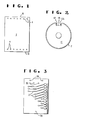
- FIG. 1 shows a magnetic film 2 which can be a layer of permanent magnetic material such as Cr0 2 particles dispersed in a binder matrix coated on a support film such as oriented polyethylene terephthalate.
- the film 2 has rows of a plurality of holes 4 adjacent the leading edge 6 and trailing edge 8 for mounting the film on a rotatable printing drum of a printing press.
- FIG. 2 shows magnetic film 2 mounted to the surface of rotatable printing drum 10 by a plurality of registration pins 12 and 12A extending from the sides of a longitudinal groove 14 in the periphery of the printing drum.
- the pins 12 and 12A are in rows, only the end pins of which are visible in FIG. 2.
- the spacing of the pins corresponds to the spacing between holes 4 in the film 2.
- These holes are conveniently punched in the magnetic film printing plate 2 by a punch which has been pre-set according to the spacing of pins 12 in each row.
- the rows of pins on the trailing edge 12A can be spring loaded so as to hold the film securely against the surface of the drum.
- the pins 12 when inserted in holes 4 in the film thus provide a predetermined positioning of the magnetic film printing plate 2 on the drum 10.
- the next step is to properly locate the latent magnetic image in the magnetic film so that registration with the receptor is ultimately achieved.
- the latent image is located in the film by sensing the position of the plurality of holes 4 in the film 2 and forming the latent image in the film at a predetermined location in response to the sensing. The location of the holes and latent image thus have a fixed known spatial relationship to each other.
- the magnetic film 2 receives its latent image of a circuit pattern either before or after mounting on the printing drum 10 by using artwork having regions of different transparency to radiation forming the desired image in the artwork.
- the artwork will be a photographic negative in which the image is defined by opaque areas and transparent areas.
- a plurality of holes 26 (See FIG. 3) is formed in the artwork corresponding to the plurality of holes 4 in film 2. This can be done by using the same punch that punched holes 4 in film 2 to punch the same or fewer holes in the artwork, which thereby registers the artwork with the film.
- FIG. 3 shows the above-described preferred embodiment of the resultant artwork 20 having a plurality of holes 26 which correspond to a plurality of holes 4 of film 2 and a plurality of additional holes 30 at a predetermined location relative to holes 26.
- the holes 26 form a row which is adjacent the corresponding leading edge of the artwork. If desired, one or more holes, indicated in phantom lines as hole 28, can be punched in the trailing edge of the artwork to correspond with a hole 4 in film 2.
- the latent image in artwork 20 can then be formed in film 2 by aligning the artwork with the film by registering holes 4 and 26, such as by the use of pins, and transferring the artwork image to the printing medium. This is accomplished by radiating the film through the artwork sufficiently to exceed the Curie temperature, which is 118°C for the preferred Cr0 2 permanent magnetic material in the film, whereby the film loses its magnetism in the area exposed to the heating up provided by the radiation.
- the relatively unheated area of the film is still magnetic and thus forms in the film a latent magnetic image of a circuit pattern 22 (schematically represented) in the artwork. This image is developed by contacting the image with magnetic toner, which adheres to the latent magnetic image.
- a computer is programmed with the image desired and the predetermined location of this image relative to a plurality of holes 4 in the film.
- This electronically stored image is then imparted to the film in conventional fashion such as by use of a scanning magnetic write head traversing the film 2 to form the latent image in the film.
- the next step in the preferred embodiment is to sense the location of holes 30 in the artwork 20 relative to pattern 22 and form a plurality of registration holes in the receptor in response to this sensing.
- holes 30 are translated by computer-controlled drilling to registration holes in the printed circuit board.
- Computer-controlled drilling is a conventional drilling operation, typically called numerically controlled (NC) drilling.
- NC numerically controlled
- An operator scans the artwork and wherever the image calls for a hole, the operator enters its coordinates in a tape, which can be a punched tape or a magnetic tape, which is the program for the drilling operation. At the time of this scan, the operator also registers the registration holes 30 in the tape. Holes 30 are then drilled in the same orientation relative to the pattern as the punched holes 30 have to image 22.
- the holes drilled in the printed circuit board which correspond to holes 30 are registration holes 38 for positioning the printed circuit board in the feeding arrangement of the printing apparatus, to thereby achieve registration between the developed image from film 2 and the printed circuit board, particularly the holes drilled therein. All these holes are at a predetermined location relative to the latent image in the film so that registration of the printed circuit board and the developed latent image is eventually possible.
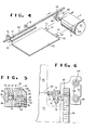
- FIG. 4 shows a stationary loading platen 40 which can be used in the feeding arrangement of the printing apparatus as the receiver for a printed circuit board.
- Platen 40 has a registration pin 42 mounted on a stationary block 41 corresponding to the location of one of the holes 30 in the artwork and one of the holes in the printed circuit board and a registration pin 44 mounted on a block 45 which can be moved laterally to correspond to another of the holes 30 in the artwork and holes of the board.
- the location of pins 42 and 44 precisely corresponds to the registration holes drilled in the printed circuit board. Accordingly, pins 42 and 44 establish a fixed known spatial relationship for the printed circuit board located on the platen by the pins and the latent image in the magnetic film.
- Block 45 is movable by virtue of a wedge-shaped (cross-section) bar 46 mounted to the downstream edge of platen 40, and block 45 having a corresponding wedge-shaped groove 48 for slidable mounting to the bar as best shown in FIG. 5.
- Block 45 also has groove 50 extending into the block from groove 48.
- a rubber strip 52 mounted in a grooved space 54.
- Cam 56 is rotatably positioned along groove 50.
- the cam has a flat face 58 and a lever 60 mounted to one end outside of block 45.
- the rubber strip 52 is compressed by the rotary position of the cam; the strip thereby biases the cam against bar 46 to lock block 45 in place. Movement of the lever 60, however, to place face 58 against the corresponding surface of spacer 54 relieves the compression thereby biasing the force of strip 52 to permit the block 45 to be relocated along bar 46.
- FIG. 4 also shows the printing drum 62 of the printing apparatus, having magnetic film 2 secured thereto by rows of pins 12 and 12A extending through corresponding holes in the film.
- Drum 62 is rotatably mounted by conventional means (not shown) and has projection 64 extending from one end and a drive gear 66 mounted to this projection. Mating with the drive gear 66 and extending to the feed position of the apparatus is a rack gear 68.
- a pair of spaced bearing carriers 70 and extending between these bearing carriers and mounted thereto are upper jaw 72 and lower jaw 74.
- Lower jaw 74 is fixedly mounted to the rack gear 68 and upper jaw 72 is movable upward and downward relative to the lower jaw 74 and is actuated by conventional means such as a double-acting air cylinder.
- FIG. 5 shows means for retracting registration pins 42 and 44.
- the pin 44 is mounted to the end of a piston 80 which is slidably mounted in a hole in block 45. This hole communicates with a cylindrical cavity 82 in the block. Positioned within the cavity is a pair of 0-ring seals 84 and 86. These seals are spaced to define an upper air space 88 and lower air space 90 within the cavity. Upper and lower air holes 92 and 94, respectively, are provided in the cavity wall.
- pressurized air is admitted through air hole 92 to upper air space 88 and the lower air space 90 is simultaneously vented.
- pressurized air is admitted through air hole 94 to air space 90 and upper air space 88 and is vented through air hole 92.
- rack gear 68 and drum 62 are rotated, pins 42 and 44 are retracted.
- Jaws 72 and 74 actuated by a pneumatic, hydraulic or spring loaded mechanism (not shown) grip an edge of circuit board, usually called “robber's edge", by jaw 72 moving toward jaw 74.
- the circuit board is placed on platen 40, with the electrically conductive layer facing the platen, and the circuit board is properly positioned on the platen by pins 42 and 44 extending through holes 38 in the board.
- the pins are slightly smaller in diameter than the diameter of holes 38 to permit the pins to fit within the holes but nevertheless accurately to position the board on the platen. In this position, the robber's edge of the board extends between jaws 72 and 74. This position is then maintained by jaws 72 and 74 firmly gripping the board edge.
- the rack gear 68 serves as the mechanical synchronizing linkage to translate the proper position of the board on the platen to registration of the board with the image in the magnetic film. Specifically, rotation of gear 66 in the direction shown in FIG. 4 causes the rack gear 68 to move toward the rotating drum 62, thus coordinating the feeding of the board with the rotation of the drum. That is, the surface speed of the gripped board is the same as the surface speed of the rotating drum.
- FIG. 6 shows more detail of the printing apparatus than FIG. 4, especially, the presence of back-up roll 100 which forms a normally closed nip 102 with drum 62. Movement of rack gear 68 towards drum 62 causes board 32, gripped by jaws 72 and 74, to pass through nip 102, which forces the board with sufficient pressure against drum 62 to cause transfer of toner from the latent image in the film 2 on the drum to the conductive layer of the board.
- Guidance of rack gear 68 and carriers 70 is provided by guide rails 104 on which sleeve bearings 106 ride contained within carriers 70.
- An example of the present invention is as follows:
Landscapes
- Engineering & Computer Science (AREA)
- Physics & Mathematics (AREA)
- General Physics & Mathematics (AREA)
- Manufacturing & Machinery (AREA)
- Microelectronics & Electronic Packaging (AREA)
- Exposure And Positioning Against Photoresist Photosensitive Materials (AREA)
Applications Claiming Priority (4)
| Application Number | Priority Date | Filing Date | Title |
|---|---|---|---|
| US9046079A | 1979-11-01 | 1979-11-01 | |
| US17426380A | 1980-08-08 | 1980-08-08 | |
| US174263 | 1980-08-08 | ||
| US90460 | 2002-03-04 |
Publications (3)
| Publication Number | Publication Date |
|---|---|
| EP0028367A2 true EP0028367A2 (de) | 1981-05-13 |
| EP0028367A3 EP0028367A3 (en) | 1983-07-20 |
| EP0028367B1 EP0028367B1 (de) | 1985-08-14 |
Family
ID=26782296
Family Applications (1)
| Application Number | Title | Priority Date | Filing Date |
|---|---|---|---|
| EP19800106470 Expired EP0028367B1 (de) | 1979-11-01 | 1980-10-23 | Ausrichtverfahren in einer Druckeinrichtung |
Country Status (10)
| Country | Link |
|---|---|
| EP (1) | EP0028367B1 (de) |
| AU (1) | AU532026B2 (de) |
| BR (1) | BR8006885A (de) |
| CA (1) | CA1150850A (de) |
| CS (1) | CS221935B2 (de) |
| DD (1) | DD153928A5 (de) |
| DE (1) | DE3070986D1 (de) |
| MX (1) | MX148046A (de) |
| PL (1) | PL227505A1 (de) |
| YU (1) | YU277780A (de) |
Family Cites Families (2)
| Publication number | Priority date | Publication date | Assignee | Title |
|---|---|---|---|---|
| GB864430A (en) * | 1958-10-23 | 1961-04-06 | Gen Electric Co Ltd | Improvements in or relating to the manufacture of printed electric circuits |
| IT953251B (it) * | 1972-02-05 | 1973-08-10 | Bieffebi Di Degli Esposti Fran | Macchina per il montaggio di matri ci flessibili su cilindri da stam pa e per prove di stampa con i ci lindri cosi preparati |
-
1980
- 1980-10-01 MX MX18415680A patent/MX148046A/es unknown
- 1980-10-23 EP EP19800106470 patent/EP0028367B1/de not_active Expired
- 1980-10-23 DE DE8080106470T patent/DE3070986D1/de not_active Expired
- 1980-10-24 CS CS720480A patent/CS221935B2/cs unknown
- 1980-10-27 PL PL22750580A patent/PL227505A1/xx unknown
- 1980-10-27 BR BR8006885A patent/BR8006885A/pt unknown
- 1980-10-30 YU YU277780A patent/YU277780A/xx unknown
- 1980-10-30 CA CA000363623A patent/CA1150850A/en not_active Expired
- 1980-10-31 DD DD22484780A patent/DD153928A5/de unknown
- 1980-10-31 AU AU64019/80A patent/AU532026B2/en not_active Ceased
Also Published As
| Publication number | Publication date |
|---|---|
| YU277780A (en) | 1983-06-30 |
| EP0028367B1 (de) | 1985-08-14 |
| EP0028367A3 (en) | 1983-07-20 |
| AU532026B2 (en) | 1983-09-15 |
| BR8006885A (pt) | 1981-05-05 |
| CS221935B2 (en) | 1983-04-29 |
| MX148046A (es) | 1983-03-08 |
| DD153928A5 (de) | 1982-02-10 |
| PL227505A1 (de) | 1981-08-21 |
| CA1150850A (en) | 1983-07-26 |
| DE3070986D1 (en) | 1985-09-19 |
| AU6401980A (en) | 1981-05-07 |
Similar Documents
| Publication | Publication Date | Title |
|---|---|---|
| JP3482544B2 (ja) | 平らな個別物品への印刷方法および装置 | |
| EP2242595A1 (de) | Druckplatten | |
| US3768619A (en) | Direct image composing machine having means to prevent pressure overload of printing characters | |
| US5317971A (en) | Pin register mounter and method of mounting flexographic plates | |
| US20150231876A1 (en) | Method and device for aligning printing plates on printing cylinders | |
| JPH0230499B2 (de) | ||
| EP0313531A3 (de) | Verfahren zum Positionieren des Druckmaterials in einer Mehrfarbensiebdruckmaschine | |
| EP0028367B1 (de) | Ausrichtverfahren in einer Druckeinrichtung | |
| US5454247A (en) | Method of and apparatus for punching and bending a lithographic plate | |
| WO1994029043A1 (en) | Method, apparatus for punching and bending plate | |
| US20140230677A1 (en) | Method of aligning a stamp to a stamp backing plate | |
| US20140230675A1 (en) | System of aligning a stamp to a stamp backing plate | |
| US5214990A (en) | Method and system for punching holes in a sheet material | |
| US20140230674A1 (en) | System for mounting a flexographic printing plate | |
| JPH0718838U (ja) | 全自動スクリーン印刷機の自動位置決めシステムにおける印刷パターンの位置合わせ装置 | |
| US20020040768A1 (en) | High pressure, solid phase-forming apparatus and process | |
| JP2578035B2 (ja) | 基板位置決め方法 | |
| US3893393A (en) | Platen alignment control | |
| US5462836A (en) | Method of manufacturing a flexographic printing plate | |
| US20140230676A1 (en) | Flexographic plate mounting | |
| JP2734574B2 (ja) | 厚膜印刷工程における基板の位置決め装置 | |
| JPH0345709B2 (de) | ||
| JP3280371B1 (ja) | パンチベンダー | |
| JPH0342264A (ja) | プリンタの記録方法 | |
| CA2063479A1 (en) | Method and system for punching holes in a sheet material |
Legal Events
| Date | Code | Title | Description |
|---|---|---|---|
| PUAI | Public reference made under article 153(3) epc to a published international application that has entered the european phase |
Free format text: ORIGINAL CODE: 0009012 |
|
| AK | Designated contracting states |
Designated state(s): BE CH DE FR GB IT LI NL SE |
|
| PUAL | Search report despatched |
Free format text: ORIGINAL CODE: 0009013 |
|
| AK | Designated contracting states |
Designated state(s): BE CH DE FR GB IT LI NL SE |
|
| 17P | Request for examination filed |
Effective date: 19830823 |
|
| ITF | It: translation for a ep patent filed | ||
| GRAA | (expected) grant |
Free format text: ORIGINAL CODE: 0009210 |
|
| AK | Designated contracting states |
Designated state(s): BE CH DE FR GB IT LI NL SE |
|
| REF | Corresponds to: |
Ref document number: 3070986 Country of ref document: DE Date of ref document: 19850919 |
|
| ET | Fr: translation filed | ||
| PLBE | No opposition filed within time limit |
Free format text: ORIGINAL CODE: 0009261 |
|
| STAA | Information on the status of an ep patent application or granted ep patent |
Free format text: STATUS: NO OPPOSITION FILED WITHIN TIME LIMIT |
|
| 26N | No opposition filed | ||
| PGFP | Annual fee paid to national office [announced via postgrant information from national office to epo] |
Ref country code: NL Payment date: 19871031 Year of fee payment: 8 |
|
| PGFP | Annual fee paid to national office [announced via postgrant information from national office to epo] |
Ref country code: DE Payment date: 19880817 Year of fee payment: 9 |
|
| PG25 | Lapsed in a contracting state [announced via postgrant information from national office to epo] |
Ref country code: GB Effective date: 19891023 |
|
| PG25 | Lapsed in a contracting state [announced via postgrant information from national office to epo] |
Ref country code: SE Effective date: 19891024 |
|
| PG25 | Lapsed in a contracting state [announced via postgrant information from national office to epo] |
Ref country code: LI Effective date: 19891031 Ref country code: CH Effective date: 19891031 Ref country code: BE Effective date: 19891031 |
|
| BERE | Be: lapsed |
Owner name: E.I. DU PONT DE NEMOURS AND CY Effective date: 19891031 |
|
| PG25 | Lapsed in a contracting state [announced via postgrant information from national office to epo] |
Ref country code: NL Effective date: 19900501 |
|
| NLV4 | Nl: lapsed or anulled due to non-payment of the annual fee | ||
| GBPC | Gb: european patent ceased through non-payment of renewal fee | ||
| PG25 | Lapsed in a contracting state [announced via postgrant information from national office to epo] |
Ref country code: FR Effective date: 19900629 |
|
| REG | Reference to a national code |
Ref country code: CH Ref legal event code: PL |
|
| PG25 | Lapsed in a contracting state [announced via postgrant information from national office to epo] |
Ref country code: DE Effective date: 19900703 |
|
| REG | Reference to a national code |
Ref country code: FR Ref legal event code: ST |
|
| EUG | Se: european patent has lapsed |
Ref document number: 80106470.0 Effective date: 19900705 |