EP0022934A1 - Dispositif d'affichage électrooptique, en particulier affichage à cristal liquide - Google Patents
Dispositif d'affichage électrooptique, en particulier affichage à cristal liquide Download PDFInfo
- Publication number
- EP0022934A1 EP0022934A1 EP80103432A EP80103432A EP0022934A1 EP 0022934 A1 EP0022934 A1 EP 0022934A1 EP 80103432 A EP80103432 A EP 80103432A EP 80103432 A EP80103432 A EP 80103432A EP 0022934 A1 EP0022934 A1 EP 0022934A1
- Authority
- EP
- European Patent Office
- Prior art keywords
- contact
- display device
- display
- elastic body
- film
- Prior art date
- Legal status (The legal status is an assumption and is not a legal conclusion. Google has not performed a legal analysis and makes no representation as to the accuracy of the status listed.)
- Withdrawn
Links
Images
Classifications
-
- G—PHYSICS
- G02—OPTICS
- G02F—OPTICAL DEVICES OR ARRANGEMENTS FOR THE CONTROL OF LIGHT BY MODIFICATION OF THE OPTICAL PROPERTIES OF THE MEDIA OF THE ELEMENTS INVOLVED THEREIN; NON-LINEAR OPTICS; FREQUENCY-CHANGING OF LIGHT; OPTICAL LOGIC ELEMENTS; OPTICAL ANALOGUE/DIGITAL CONVERTERS
- G02F1/00—Devices or arrangements for the control of the intensity, colour, phase, polarisation or direction of light arriving from an independent light source, e.g. switching, gating or modulating; Non-linear optics
- G02F1/01—Devices or arrangements for the control of the intensity, colour, phase, polarisation or direction of light arriving from an independent light source, e.g. switching, gating or modulating; Non-linear optics for the control of the intensity, phase, polarisation or colour
- G02F1/13—Devices or arrangements for the control of the intensity, colour, phase, polarisation or direction of light arriving from an independent light source, e.g. switching, gating or modulating; Non-linear optics for the control of the intensity, phase, polarisation or colour based on liquid crystals, e.g. single liquid crystal display cells
- G02F1/133—Constructional arrangements; Operation of liquid crystal cells; Circuit arrangements
- G02F1/1333—Constructional arrangements; Manufacturing methods
- G02F1/1345—Conductors connecting electrodes to cell terminals
-
- H—ELECTRICITY
- H05—ELECTRIC TECHNIQUES NOT OTHERWISE PROVIDED FOR
- H05K—PRINTED CIRCUITS; CASINGS OR CONSTRUCTIONAL DETAILS OF ELECTRIC APPARATUS; MANUFACTURE OF ASSEMBLAGES OF ELECTRICAL COMPONENTS
- H05K3/00—Apparatus or processes for manufacturing printed circuits
- H05K3/36—Assembling printed circuits with other printed circuits
- H05K3/361—Assembling flexible printed circuits with other printed circuits
- H05K3/365—Assembling flexible printed circuits with other printed circuits by abutting, i.e. without alloying process
Definitions
- the invention relates to a display device according to the preamble of claim 1.
- a display device is known for example from "Electronics", 07.07.77, pages 96 to 103.
- Plugs create a fairly secure contact, but are relatively complex, have a bulky design and are often out of the question because they only allow certain positions between the parts to be contacted.
- elastic "zebra" strips are therefore preferred, which, as described in the cited publication, consist of alternating conductive and insulating sections and are simply clamped between the components to be connected.
- Such guide rubbers also provide a satisfactory contact, are quite compact and simple, but still leave little scope for the choice of the contact arrangement. Accordingly, it is not uncommon to rely on custom-made products, a circumstance that cannot be accepted, especially for inexpensive mass-produced items, which now also include liquid crystal displays.
- the contact film of a display device permits a wide variety of relative positions between the cell and the circuit board, since it is flexible and can even be bent without fear of deterioration of the contact you can easily create any trace configuration by electrical RF burnout and / or masking during film deposition. It is also no problem to connect contact strips with different contact spacings. Particularly fine conductor structures, such as those required for the connection of liquid crystal displays, can be worked out by an RF burnout process in which the focal point is guided by a computer-controlled digital plotter. Otherwise, one can fall back on the same techniques with which Kapton-based heating foils are already being produced (cf. the section on LCD heaters in the literature mentioned at the beginning).
- the contact foils can also be conveniently produced in large dimensions and can consist of thermally adapted materials, so that contact is not endangered at any point even under elevated operating temperatures.
- the contact foil is pressed against the display or control part plate by an elastic body, which has no electrical function and can be a simple rubber part. Under certain circumstances - such as when the display device is not exposed to mechanical shocks - such repositories could also be dispensed with.
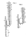
- Fig. 1 shows a liquid crystal display device with a display cell 1, a control unit 2 and a contact sheet 3.
- Cell contains two mutually parallel plates 6, 7, which each carry electrically conductive coverings (separately controllable front electrodes 8, back electrode 9) on their mutually facing sides and are tightly connected to one another via a frame 11.
- the chamber bounded by the frame and the two plates is filled with a liquid crystal layer 12.
- the leads to the individual electrodes (Electrode leads 13) begin at contact points which are equidistantly adjacent to one another in the usual manner on the inside edge of one of the two plates.
- the control unit 2 comprises a circuit board 14 on which an integrated circuit 16 is fastened. From this circuit go connection. lines 17, which also open in a row of adjacent contact points.
- the U-shaped contact foil 3, which is provided with conductor tracks 18, is clamped between the two contact strips. The film occupies a position in which its conductor tracks lie against the respective contact points.
- FIG. 2 differs from the described embodiment essentially in that the U-shaped contact foil encloses a pressure rubber 4 with a rectangular profile on three sides.
- the elastic bearing supports that the contact is particularly robust and reliable.
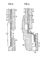
- FIGS. 3 and 4 are examples of the fact that the same film permits a wide variety of spatial assignments between the cell and the circuit board.
- the contact strips of both parts are in the same plane, but at different heights; 4 shows that the contact strips can lie both at different heights and in mutually offset planes.
- the film can be also run along a wall part or along the interface of an inaccessible space (this space is shown hatched in FIG. 4 and designated 19).
- the invention is not restricted to the exemplary embodiments shown.
- other display types are also possible, which can be switched in areas between optically different states and accordingly have several connections. It does not matter whether the display is controlled statically or in a time-division multiplex process. There is also considerable scope in terms of design.
- the display can also be provided with a plurality of contact strips, which are then each to be connected to the control module with a film. The advantages of the proposed solution come into play especially when the plates to be contacted are inclined to each other.
Landscapes
- Physics & Mathematics (AREA)
- Nonlinear Science (AREA)
- Mathematical Physics (AREA)
- Chemical & Material Sciences (AREA)
- Crystallography & Structural Chemistry (AREA)
- General Physics & Mathematics (AREA)
- Optics & Photonics (AREA)
- Liquid Crystal (AREA)
- Devices For Indicating Variable Information By Combining Individual Elements (AREA)
Applications Claiming Priority (2)
| Application Number | Priority Date | Filing Date | Title |
|---|---|---|---|
| DE7920579 | 1979-07-18 | ||
| DE7920579U | 1979-07-18 |
Publications (1)
| Publication Number | Publication Date |
|---|---|
| EP0022934A1 true EP0022934A1 (fr) | 1981-01-28 |
Family
ID=6705849
Family Applications (1)
| Application Number | Title | Priority Date | Filing Date |
|---|---|---|---|
| EP80103432A Withdrawn EP0022934A1 (fr) | 1979-07-18 | 1980-06-19 | Dispositif d'affichage électrooptique, en particulier affichage à cristal liquide |
Country Status (2)
| Country | Link |
|---|---|
| EP (1) | EP0022934A1 (fr) |
| JP (1) | JPS5617322A (fr) |
Cited By (10)
| Publication number | Priority date | Publication date | Assignee | Title |
|---|---|---|---|---|
| EP0083253A2 (fr) * | 1981-12-28 | 1983-07-06 | Seiko Epson Corporation | Appareil optique d'impression à cristaux liquides |
| DE3243227A1 (de) * | 1982-11-23 | 1984-05-24 | Licentia Patent-Verwaltungs-Gmbh, 6000 Frankfurt | Verfahren zum herstellen einer fluessigkristall-anzeigevorrichtung |
| DE3431077A1 (de) * | 1983-08-24 | 1985-03-14 | Sharp K.K., Osaka | Treiberanordnung fuer ein flachmatrixdisplay |
| GB2155368A (en) * | 1982-08-03 | 1985-09-25 | Burroughs Corp | Method and apparatus for correcting printed circuit boards |
| GB2155382A (en) * | 1982-08-03 | 1985-09-25 | Burroughs Corp | Stitch welding of wire to a printed circuit board |
| EP0168228A3 (en) * | 1984-07-06 | 1987-07-15 | Sharp Kabushiki Kaisha | Display device |
| US4690510A (en) * | 1982-07-13 | 1987-09-01 | Sharp Kabushiki Kaisha | Structure and method of connecting terminals of matrix display units |
| US4772100A (en) * | 1986-10-09 | 1988-09-20 | Oki Electric Industry Co. Ltd. | Liquid crystal display device having circuit boards extending along segment and column electrode directions |
| WO1988008551A1 (fr) * | 1987-04-30 | 1988-11-03 | N-View Corporation | Affichage a cristaux liquides pour systemes de projection |
| GB2251344A (en) * | 1990-12-03 | 1992-07-01 | Rheinmetall Gmbh | Connecting surface mount devices to printed circuit boards. |
Families Citing this family (1)
| Publication number | Priority date | Publication date | Assignee | Title |
|---|---|---|---|---|
| JPS59231518A (ja) * | 1983-06-14 | 1984-12-26 | Matsushita Electric Ind Co Ltd | 液晶とプリント基板の接続装置 |
Citations (2)
| Publication number | Priority date | Publication date | Assignee | Title |
|---|---|---|---|---|
| US3718842A (en) * | 1972-04-21 | 1973-02-27 | Texas Instruments Inc | Liquid crystal display mounting structure |
| DE2427335A1 (de) * | 1973-06-06 | 1975-01-02 | Sharp Kk | Tragbarer elektronischer rechner |
-
1980
- 1980-06-19 EP EP80103432A patent/EP0022934A1/fr not_active Withdrawn
- 1980-07-17 JP JP9815280A patent/JPS5617322A/ja active Pending
Patent Citations (2)
| Publication number | Priority date | Publication date | Assignee | Title |
|---|---|---|---|---|
| US3718842A (en) * | 1972-04-21 | 1973-02-27 | Texas Instruments Inc | Liquid crystal display mounting structure |
| DE2427335A1 (de) * | 1973-06-06 | 1975-01-02 | Sharp Kk | Tragbarer elektronischer rechner |
Non-Patent Citations (1)
| Title |
|---|
| SOLID-STATE TECHNOLOGY, Vol. 22, No. 1, January 1979, Washington, J. MARSHALL et al.: "Solder Bump Interconnected, Multiple Chip, Thick Film Hybrid for 40-Character Alpha-numeric LCD Application", Seiten 87 bis 93. * |
Cited By (14)
| Publication number | Priority date | Publication date | Assignee | Title |
|---|---|---|---|---|
| EP0083253A2 (fr) * | 1981-12-28 | 1983-07-06 | Seiko Epson Corporation | Appareil optique d'impression à cristaux liquides |
| EP0083253A3 (fr) * | 1981-12-28 | 1985-10-23 | Seiko Epson Corporation | Appareil optique d'impression à cristaux liquides |
| US4690510A (en) * | 1982-07-13 | 1987-09-01 | Sharp Kabushiki Kaisha | Structure and method of connecting terminals of matrix display units |
| GB2155382A (en) * | 1982-08-03 | 1985-09-25 | Burroughs Corp | Stitch welding of wire to a printed circuit board |
| GB2155368A (en) * | 1982-08-03 | 1985-09-25 | Burroughs Corp | Method and apparatus for correcting printed circuit boards |
| EP0111734A3 (en) * | 1982-11-23 | 1985-02-13 | Licentia Patent-Verwaltungs-Gmbh | Method of manufacturing a liquid crystal display device |
| EP0111734A2 (fr) * | 1982-11-23 | 1984-06-27 | Licentia Patent-Verwaltungs-GmbH | Procédé de fabrication d'un dispostif d'affichage à cristal liquide |
| DE3243227A1 (de) * | 1982-11-23 | 1984-05-24 | Licentia Patent-Verwaltungs-Gmbh, 6000 Frankfurt | Verfahren zum herstellen einer fluessigkristall-anzeigevorrichtung |
| DE3431077A1 (de) * | 1983-08-24 | 1985-03-14 | Sharp K.K., Osaka | Treiberanordnung fuer ein flachmatrixdisplay |
| EP0168228A3 (en) * | 1984-07-06 | 1987-07-15 | Sharp Kabushiki Kaisha | Display device |
| US4772100A (en) * | 1986-10-09 | 1988-09-20 | Oki Electric Industry Co. Ltd. | Liquid crystal display device having circuit boards extending along segment and column electrode directions |
| WO1988008551A1 (fr) * | 1987-04-30 | 1988-11-03 | N-View Corporation | Affichage a cristaux liquides pour systemes de projection |
| GB2251344A (en) * | 1990-12-03 | 1992-07-01 | Rheinmetall Gmbh | Connecting surface mount devices to printed circuit boards. |
| GB2251344B (en) * | 1990-12-03 | 1994-11-16 | Rheinmetall Gmbh | Connection of devices to printed circuit boards |
Also Published As
| Publication number | Publication date |
|---|---|
| JPS5617322A (en) | 1981-02-19 |
Similar Documents
| Publication | Publication Date | Title |
|---|---|---|
| DE3616046C2 (de) | Flüssigkristall-Anzeigevorrichtung mit einer Leiterplatte | |
| EP0013335A1 (fr) | Installation pour connecter électriquement une pluralité de contacts | |
| DE2512417B2 (de) | Elektronische uhr mit elektrooptischer anzeigevorrichtung und integrierter schaltung | |
| DE2511252A1 (de) | Optische wiedergabeeinrichtung | |
| DE2534697A1 (de) | Anzeigeeinrichtung | |
| DE3325315A1 (de) | Matrixanzeige | |
| EP0022934A1 (fr) | Dispositif d'affichage électrooptique, en particulier affichage à cristal liquide | |
| CH667562A5 (de) | Verfahren zum aendern einer elektrischen flachbaugruppe. | |
| EP0594987B1 (fr) | Module électrique | |
| DE3530827C2 (fr) | ||
| DE3743841C2 (fr) | ||
| DE7920579U1 (de) | Elektrooptische Anzeigevorrichtung, insbesondere Flüssigkristallanzeige | |
| DE2910779A1 (de) | Anzeigebaustein mit einer elektrooptischen anzeigevorrichtung | |
| EP0019667A1 (fr) | Dispositif de fixation d'une cellule d'affichage à cristaux liquides sur une plaque de support | |
| EP0289654A2 (fr) | Procédé de soudage des terminaisons d'un composant électronique et feuille utilisée dans la réalisation du procédé | |
| DE2625726B2 (de) | Elektronische Kleinuhr | |
| DE2649566B2 (de) | Elektronischer Rechner mit einer mehrziffrigen Anzeigeeinrichtung | |
| DE3143174C2 (de) | Klemmvorrichtung zum Kontaktieren von elektrischen Kontaktstellen auf Leiterplatten | |
| DE4416096A1 (de) | Kontaktierung von Betätigungs- und Anzeigemitteln | |
| DE2434675C2 (de) | Elektronische Armbanduhr | |
| DE2547426C3 (de) | Tastenschalter | |
| DE3313080A1 (de) | Vorrichtung zum kontaktieren einer anzeigeeinheit mit fluessigkristallschicht | |
| DE19642230C1 (de) | Anzeigeeinheit mit einem hinterleuchteten LC-Display | |
| DE8122278U1 (de) | Elektro-optische Anzeigevorrichtung mit einem Halterungsrahmen | |
| DE3426715A1 (de) | Vorrichtung zur anzeige von messwerten |
Legal Events
| Date | Code | Title | Description |
|---|---|---|---|
| PUAI | Public reference made under article 153(3) epc to a published international application that has entered the european phase |
Free format text: ORIGINAL CODE: 0009012 |
|
| AK | Designated contracting states |
Designated state(s): CH FR GB IT NL |
|
| STAA | Information on the status of an ep patent application or granted ep patent |
Free format text: STATUS: THE APPLICATION IS DEEMED TO BE WITHDRAWN |
|
| 18D | Application deemed to be withdrawn |
Effective date: 19820102 |
|
| RIN1 | Information on inventor provided before grant (corrected) |
Inventor name: SLOWIOCZEK, AUGUSTIN, ING.-GRAD. Inventor name: KARZMARZYK, MANFRED, DIPL.-ING. |