EP0022934A1 - Electrooptical display device, especially liquid crystal display - Google Patents
Electrooptical display device, especially liquid crystal display Download PDFInfo
- Publication number
- EP0022934A1 EP0022934A1 EP80103432A EP80103432A EP0022934A1 EP 0022934 A1 EP0022934 A1 EP 0022934A1 EP 80103432 A EP80103432 A EP 80103432A EP 80103432 A EP80103432 A EP 80103432A EP 0022934 A1 EP0022934 A1 EP 0022934A1
- Authority
- EP
- European Patent Office
- Prior art keywords
- contact
- display device
- display
- elastic body
- film
- Prior art date
- Legal status (The legal status is an assumption and is not a legal conclusion. Google has not performed a legal analysis and makes no representation as to the accuracy of the status listed.)
- Withdrawn
Links
Images
Classifications
-
- G—PHYSICS
- G02—OPTICS
- G02F—OPTICAL DEVICES OR ARRANGEMENTS FOR THE CONTROL OF LIGHT BY MODIFICATION OF THE OPTICAL PROPERTIES OF THE MEDIA OF THE ELEMENTS INVOLVED THEREIN; NON-LINEAR OPTICS; FREQUENCY-CHANGING OF LIGHT; OPTICAL LOGIC ELEMENTS; OPTICAL ANALOGUE/DIGITAL CONVERTERS
- G02F1/00—Devices or arrangements for the control of the intensity, colour, phase, polarisation or direction of light arriving from an independent light source, e.g. switching, gating or modulating; Non-linear optics
- G02F1/01—Devices or arrangements for the control of the intensity, colour, phase, polarisation or direction of light arriving from an independent light source, e.g. switching, gating or modulating; Non-linear optics for the control of the intensity, phase, polarisation or colour
- G02F1/13—Devices or arrangements for the control of the intensity, colour, phase, polarisation or direction of light arriving from an independent light source, e.g. switching, gating or modulating; Non-linear optics for the control of the intensity, phase, polarisation or colour based on liquid crystals, e.g. single liquid crystal display cells
- G02F1/133—Constructional arrangements; Operation of liquid crystal cells; Circuit arrangements
- G02F1/1333—Constructional arrangements; Manufacturing methods
- G02F1/1345—Conductors connecting electrodes to cell terminals
-
- H—ELECTRICITY
- H05—ELECTRIC TECHNIQUES NOT OTHERWISE PROVIDED FOR
- H05K—PRINTED CIRCUITS; CASINGS OR CONSTRUCTIONAL DETAILS OF ELECTRIC APPARATUS; MANUFACTURE OF ASSEMBLAGES OF ELECTRICAL COMPONENTS
- H05K3/00—Apparatus or processes for manufacturing printed circuits
- H05K3/36—Assembling printed circuits with other printed circuits
- H05K3/361—Assembling flexible printed circuits with other printed circuits
- H05K3/365—Assembling flexible printed circuits with other printed circuits by abutting, i.e. without alloying process
Definitions
- the invention relates to a display device according to the preamble of claim 1.
- a display device is known for example from "Electronics", 07.07.77, pages 96 to 103.
- Plugs create a fairly secure contact, but are relatively complex, have a bulky design and are often out of the question because they only allow certain positions between the parts to be contacted.
- elastic "zebra" strips are therefore preferred, which, as described in the cited publication, consist of alternating conductive and insulating sections and are simply clamped between the components to be connected.
- Such guide rubbers also provide a satisfactory contact, are quite compact and simple, but still leave little scope for the choice of the contact arrangement. Accordingly, it is not uncommon to rely on custom-made products, a circumstance that cannot be accepted, especially for inexpensive mass-produced items, which now also include liquid crystal displays.
- the contact film of a display device permits a wide variety of relative positions between the cell and the circuit board, since it is flexible and can even be bent without fear of deterioration of the contact you can easily create any trace configuration by electrical RF burnout and / or masking during film deposition. It is also no problem to connect contact strips with different contact spacings. Particularly fine conductor structures, such as those required for the connection of liquid crystal displays, can be worked out by an RF burnout process in which the focal point is guided by a computer-controlled digital plotter. Otherwise, one can fall back on the same techniques with which Kapton-based heating foils are already being produced (cf. the section on LCD heaters in the literature mentioned at the beginning).
- the contact foils can also be conveniently produced in large dimensions and can consist of thermally adapted materials, so that contact is not endangered at any point even under elevated operating temperatures.
- the contact foil is pressed against the display or control part plate by an elastic body, which has no electrical function and can be a simple rubber part. Under certain circumstances - such as when the display device is not exposed to mechanical shocks - such repositories could also be dispensed with.
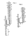
- Fig. 1 shows a liquid crystal display device with a display cell 1, a control unit 2 and a contact sheet 3.
- Cell contains two mutually parallel plates 6, 7, which each carry electrically conductive coverings (separately controllable front electrodes 8, back electrode 9) on their mutually facing sides and are tightly connected to one another via a frame 11.
- the chamber bounded by the frame and the two plates is filled with a liquid crystal layer 12.
- the leads to the individual electrodes (Electrode leads 13) begin at contact points which are equidistantly adjacent to one another in the usual manner on the inside edge of one of the two plates.
- the control unit 2 comprises a circuit board 14 on which an integrated circuit 16 is fastened. From this circuit go connection. lines 17, which also open in a row of adjacent contact points.
- the U-shaped contact foil 3, which is provided with conductor tracks 18, is clamped between the two contact strips. The film occupies a position in which its conductor tracks lie against the respective contact points.
- FIG. 2 differs from the described embodiment essentially in that the U-shaped contact foil encloses a pressure rubber 4 with a rectangular profile on three sides.
- the elastic bearing supports that the contact is particularly robust and reliable.
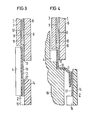
- FIGS. 3 and 4 are examples of the fact that the same film permits a wide variety of spatial assignments between the cell and the circuit board.
- the contact strips of both parts are in the same plane, but at different heights; 4 shows that the contact strips can lie both at different heights and in mutually offset planes.
- the film can be also run along a wall part or along the interface of an inaccessible space (this space is shown hatched in FIG. 4 and designated 19).
- the invention is not restricted to the exemplary embodiments shown.
- other display types are also possible, which can be switched in areas between optically different states and accordingly have several connections. It does not matter whether the display is controlled statically or in a time-division multiplex process. There is also considerable scope in terms of design.
- the display can also be provided with a plurality of contact strips, which are then each to be connected to the control module with a film. The advantages of the proposed solution come into play especially when the plates to be contacted are inclined to each other.
Abstract
Description
Die Erfindung betrifft eine Anzeigevorrichtung gemäß dem Oberbegriff des Anspruchs 1. Ein solches Display ist beispielsweise aus "Electronics", 07.07.77, Seiten 96 bis 103, bekannt.The invention relates to a display device according to the preamble of claim 1. Such a display is known for example from "Electronics", 07.07.77, pages 96 to 103.
Wenn der elektrische Kontakt zwischen der eigent-. lichen'Anzeigezelle und der zugehörigen Ansteuereinheit lösbar gestaltet sein soll, so bietet es sich an, beide Teile durch eine Steckerleiste miteinander zu verbinden. Stecker schaffen einen recht sicheren Kontakt, sind jedoch relativ kompliziert aufgebaut, haben zudem eine sperrige Bauform und kommen häufig schon deshalb nicht in Frage, weil sie nur ganz bestimmte Lagen zwischen den zu kontaktierenden Teilen zulassen. Man zieht daher in vielen Fällen elastische "Zebra"-Streifen vor, die, wie in der zitierten Veröffentlichung beschrieben, abwechselnd aus leitenden und isolierenden Abschnitten bestehen und einfach zwischen die zu verbindenden Bauteile geklemmt werden. Solche Leitgummis liefern ebenfalls einen zufriedenstellenden Kontakt, sind dabei recht kompakt und einfach ausgeführt, lassen aber nach wie vor nur einen geringen Spielraum bei der Wahl der Kontaktanordnung zu. Dementsprechend ist man nicht selten auf Sonderfertigen angewiesen, ein Umstand, der vor allem bei preiswerten Massenartikeln zu denen inzwischen auch Flüssigkristallanzeigen gehören, nicht akzeptiert werden kann.If the electrical contact between the actual. If the display cell and the associated control unit are designed to be detachable, it makes sense to connect the two parts to one another by means of a plug connector. Plugs create a fairly secure contact, but are relatively complex, have a bulky design and are often out of the question because they only allow certain positions between the parts to be contacted. In many cases, elastic "zebra" strips are therefore preferred, which, as described in the cited publication, consist of alternating conductive and insulating sections and are simply clamped between the components to be connected. Such guide rubbers also provide a satisfactory contact, are quite compact and simple, but still leave little scope for the choice of the contact arrangement. Accordingly, it is not uncommon to rely on custom-made products, a circumstance that cannot be accepted, especially for inexpensive mass-produced items, which now also include liquid crystal displays.
Es fehlt demnach noch immer an einem elektrischen Verbinder, der kostengünstig hergestellt werden kann, dabei eine zuverlässige Kontaktierung gewährleistet und zudem eine in weiten Grenzen frei wählbare Kontaktgeometrie zuläßt. Um diese Lücke zu schließen, wird erfindungsgemäß ein Display mit den Merkmalen des Patentanspruchs 1 vorgeschlagen.Accordingly, there is still a lack of an electrical connector which can be produced inexpensively, thereby ensuring reliable contacting and, moreover, permitting a freely selectable contact geometry. To close this gap, a display with the features of claim 1 is proposed according to the invention.
Die Kontaktfolie einer erfindungsgemäßen Anzeigevorrichtung'läßt die verschiedensten Relativlagen zwischen Zelle und Platine zu, da sie biegsam ist und sogar geknickt werden kann, ohne daß man eine Kontaktverschlechterung befürchten müßte..Darüber hinaus gibt die Folienfertigung keinerlei Probleme auf, denn man kann beliebige Leiterbahnkonfigurationen ohne weiteres durch elektrisches HF-Ausbrennen und/oder Abdecken bei der Folienbedampfung erzeugen. So bereitet es auch keinerlei Schwierigkeiten, Kontaktleisten mit voneinander'differierenden Kontaktabständen miteinander zu verbinden. Besonders feine Leiterstrukturen, wie sie beispielsweise für den Anschluß von Flüssigkristalldisplays erforderlich sind, lassen sich durch.einen HF-Ausbrenn-ProzeB herausarbeiten, bei dem die Brennstelle durch einen Rechner-gesteuerten Digital-Plotter geführt wird. Im übrigen kann man auf die gleichen Techniken zurückgreifen, mit denen bereits Heizfolien auf Kapton-Basis erzeugt werden (vergl. hierzu in der eingangs erwähnten Literaturstelle den Abschnitt LCD-Heaters). Die Kontaktfolien sind auch in großen Abmessungen bequem herstellbar und können aus thermisch angepaßten Werkstoffen bestehen, so daß die Kontaktgabe auch unter erhöhten Betriebstemperaturen an keiner Stelle gefährdet ist.The contact film of a display device according to the invention permits a wide variety of relative positions between the cell and the circuit board, since it is flexible and can even be bent without fear of deterioration of the contact you can easily create any trace configuration by electrical RF burnout and / or masking during film deposition. It is also no problem to connect contact strips with different contact spacings. Particularly fine conductor structures, such as those required for the connection of liquid crystal displays, can be worked out by an RF burnout process in which the focal point is guided by a computer-controlled digital plotter. Otherwise, one can fall back on the same techniques with which Kapton-based heating foils are already being produced (cf. the section on LCD heaters in the literature mentioned at the beginning). The contact foils can also be conveniently produced in large dimensions and can consist of thermally adapted materials, so that contact is not endangered at any point even under elevated operating temperatures.
In der Regel wird die Kontaktfolie durch einen elastischen Körper, der keine elektrische Funktion erfüllt und ein einfaches Gümmiteil sein kann, an die Display- bzw. Steuerteilplatte gedrückt. Unter bestimmten Umständen - wenn etwa die Anzeigevorrichtung keinen mechanischen Erschütterungen ausgesetzt ist - könnte man auf solche Wiederlager auch verzichten.As a rule, the contact foil is pressed against the display or control part plate by an elastic body, which has no electrical function and can be a simple rubber part. Under certain circumstances - such as when the display device is not exposed to mechanical shocks - such repositories could also be dispensed with.
Weitere vorteilhafte Ausgestaltungen und Weiterbildungen der Erfindung sind Gegenstand zusätzlicher Ansprüche.Further advantageous refinements and developments of the invention are the subject of additional claims.
Der Lösungsvorschlag soll nun anhand von vier bevorzugten Ausführungsbeispielen in Verbindung mit der . beigefügten Zeichnung näher erläutert werden. In den Figuren sind einander entsprechende Teile mit gleichen Bezugszeichen versehen. Es zeigen:
- Fig. 1 ein erstes Ausführungsbeispiel in einem Seitenschnitt
- Fig. 2 in einem teilweise weggebrochenen Seitenschnittein zweites Ausführungsbeispiel und
- Fig. 3 und 4 in der gleichen Darstellungsweise wie bei Fig. 1 weitere Ausführungsbeispiele.
- Fig. 1 shows a first embodiment in a side section
- Fig. 2 in a partially cut-away side section in a second embodiment and
- 3 and 4 in the same representation as in Fig. 1 further embodiments.
Die Figuren sind der Übersicht halber sehr schematisch gehalten. So fehlen beispielsweise Halterungs- und Klemmelemente oder einzelne Zuleitungen, also Einzelteile, die für ein Verständnis der Erfindung nicht unbedingt erforderlich sind.For the sake of clarity, the figures are kept very schematic. For example, mounting and clamping elements or individual feed lines, i.e. individual parts, which are not absolutely necessary for an understanding of the invention, are missing.
Die Fig. 1 zeigt eine Flüssigkristall-Anzeigevorrichtung mit einer Anzeigezelle 1, einer Ansteuereinheit 2 und einer Kontaktfolie 3. Die Anzeige- . zelle enthält zwei zueinander parallele Platten 6,7, die auf ihren einander zugewandten Seiten jeweils elektrisch leitende Beläge (getrennt ansteuerbare Vorderelektroden 8, Rückelektrode 9) tragen und über einen Rahmen 11 dicht miteinander verbunden sind. Die vom Rahmen und den beiden Platten begrenzte Kammer ist mit einer Flüssigkristallschicht 12 gefüllt. Die Zuleitungen zu den einzelnen Elektroden (Elektrodenzuleitungen 13) nehmen ihren Anfang in Kontaktstellen, die in üblicher Weise auf dem Innenseitenrand einer der beiden Platten äquidistant nebeneinanderliegen. Die Ansteuereinheit 2 umfaßt eine Platine 14, auf der eine integrierte Schaltung 16 befestigt ist. Von dieser Schaltung gehen Verbindungs-. leitungen 17 aus, die ebenfalls in einer Reihe aus nebeneinanderliegenden Kontaktstellen münden. Zwischen beide Kontaktleisten ist die mit Leiterbahnen 18 versehene, u-förmig gebogene Kontaktfolie 3 eingeklemmt. Die Folie nimmt dabei eine Position ein, in der ihre Leiterbahnen den jeweiligen Kontaktstellen anliegen.Fig. 1 shows a liquid crystal display device with a display cell 1, a
Das Ausführungsbeispiel der Fig. 2-unterscheidet sich von der geschilderten Ausführung im wesentlichen darin, daß die u-förmig gebogene Kontaktfolie ein Andruckgummi 4 mit rechteckigem Pofil an drei Seiten umschließt. Das elastische Wiederlager trägt dazu bei, daß der Kontakt besonders robust und zuverlässig ist.The embodiment of FIG. 2 differs from the described embodiment essentially in that the U-shaped contact foil encloses a pressure rubber 4 with a rectangular profile on three sides. The elastic bearing supports that the contact is particularly robust and reliable.
Die in den Figuren 3 und 4 dargestellten Anzeigeversinnen sind Beispiele dafür, daß die gleiche Folie die verschiedensten räumlichen Zuordnungen zwischen Zelle und Platine gestattet. Bei der Variante der Fig. 3 befinden sich die Kontaktleisten beider Teile in der gleichen Ebene, jedoch auf verschiedenen Höhen; in Fig. 4 ist gezeigt, daß die Kontaktleisten sowohl in unterschiedlichen Höhen als auch in zueinander versetzten Ebenen liegen können. Die Folie läßt sich dabei auch entlang eines Wandungsteils oder längs der Grenzfläche eines nicht zugänglichen Raumes führen (dieser Raum ist in Fig. 4 schraffiert eingezeichnet und mit 19 bezeichnet).The display intentions shown in FIGS. 3 and 4 are examples of the fact that the same film permits a wide variety of spatial assignments between the cell and the circuit board. In the variant of Figure 3, the contact strips of both parts are in the same plane, but at different heights; 4 shows that the contact strips can lie both at different heights and in mutually offset planes. The film can be also run along a wall part or along the interface of an inaccessible space (this space is shown hatched in FIG. 4 and designated 19).
Die Kontaktfolie kann folgendermaßen hergestellt werden:
- Auf ein Kapton-Substrat wird eine Metallschicht aufgedampft, aus der dann einzelne Leiterbahnen mit definierten Pfaden, Abständen und Breiten herausgebrannt werden. Hierzu führt man mit einem Tischrechner-gesteuerten Digital-Plotter eine Nadel, die einen definierten Durchmesser hat und die benötigte Ausbrennenergie durch einen angeschlossenen HF-Generator erhält.
- A metal layer is vapor-deposited onto a Kapton substrate, from which individual conductor tracks with defined paths, distances and widths are then burned out. To do this, a table computer-controlled digital plotter is used to guide a needle that has a defined diameter and receives the required burnout energy from a connected HF generator.
Die Erfindung ist nicht auf die dargestellten Ausführungsbeispiele beschränkt. So kommen neben Flüssigkristallanzeigen auch andere Displaytypen infrage, die bereichsweise zwischen optisch verschiedenen Zuständen geschaltet werden können und dementsprechend über mehrere Anschlüsse verfügen. Dabei spielt es keine Rolle, ob die Anzeige statisch oder in einem Zeitmultiplexverfahren angesteuert wird. Auch in konstruktiver Hinsicht besteht noch ein erheblicher Spielraum. So kann das Display auch mit mehreren Kontaktleisten versehen sein, die dann jeweils mit einer Folie an den Ansteuermodul anzuschließen sind. Die Vorzüge des Lösungsvorschlags kommen vor allem dann zum Tragen, wenn die miteinander zu kontaktierenden Platten zueinander geneigt sind..The invention is not restricted to the exemplary embodiments shown. In addition to liquid crystal displays, other display types are also possible, which can be switched in areas between optically different states and accordingly have several connections. It does not matter whether the display is controlled statically or in a time-division multiplex process. There is also considerable scope in terms of design. Thus, the display can also be provided with a plurality of contact strips, which are then each to be connected to the control module with a film. The advantages of the proposed solution come into play especially when the plates to be contacted are inclined to each other.
Claims (3)
dadurch gekennzeichnet , daß
characterized in that
Applications Claiming Priority (2)
| Application Number | Priority Date | Filing Date | Title |
|---|---|---|---|
| DE7920579 | 1979-07-18 | ||
| DE7920579U | 1979-07-18 |
Publications (1)
| Publication Number | Publication Date |
|---|---|
| EP0022934A1 true EP0022934A1 (en) | 1981-01-28 |
Family
ID=6705849
Family Applications (1)
| Application Number | Title | Priority Date | Filing Date |
|---|---|---|---|
| EP80103432A Withdrawn EP0022934A1 (en) | 1979-07-18 | 1980-06-19 | Electrooptical display device, especially liquid crystal display |
Country Status (2)
| Country | Link |
|---|---|
| EP (1) | EP0022934A1 (en) |
| JP (1) | JPS5617322A (en) |
Cited By (10)
| Publication number | Priority date | Publication date | Assignee | Title |
|---|---|---|---|---|
| EP0083253A2 (en) * | 1981-12-28 | 1983-07-06 | Seiko Epson Corporation | Liquid crystal optical printing apparatus |
| DE3243227A1 (en) * | 1982-11-23 | 1984-05-24 | Licentia Patent-Verwaltungs-Gmbh, 6000 Frankfurt | METHOD FOR PRODUCING A LIQUID CRYSTAL DISPLAY DEVICE |
| DE3431077A1 (en) * | 1983-08-24 | 1985-03-14 | Sharp K.K., Osaka | DRIVER ARRANGEMENT FOR A FLAT MATRIX DISPLAY |
| GB2155368A (en) * | 1982-08-03 | 1985-09-25 | Burroughs Corp | Method and apparatus for correcting printed circuit boards |
| GB2155382A (en) * | 1982-08-03 | 1985-09-25 | Burroughs Corp | Stitch welding of wire to a printed circuit board |
| EP0168228A3 (en) * | 1984-07-06 | 1987-07-15 | Sharp Kabushiki Kaisha | Display device |
| US4690510A (en) * | 1982-07-13 | 1987-09-01 | Sharp Kabushiki Kaisha | Structure and method of connecting terminals of matrix display units |
| US4772100A (en) * | 1986-10-09 | 1988-09-20 | Oki Electric Industry Co. Ltd. | Liquid crystal display device having circuit boards extending along segment and column electrode directions |
| WO1988008551A1 (en) * | 1987-04-30 | 1988-11-03 | N-View Corporation | Liquid crystal display for projection systems |
| GB2251344A (en) * | 1990-12-03 | 1992-07-01 | Rheinmetall Gmbh | Connecting surface mount devices to printed circuit boards. |
Families Citing this family (1)
| Publication number | Priority date | Publication date | Assignee | Title |
|---|---|---|---|---|
| JPS59231518A (en) * | 1983-06-14 | 1984-12-26 | Matsushita Electric Ind Co Ltd | Connecting device between liquid crystal and printed circuit board |
Citations (2)
| Publication number | Priority date | Publication date | Assignee | Title |
|---|---|---|---|---|
| US3718842A (en) * | 1972-04-21 | 1973-02-27 | Texas Instruments Inc | Liquid crystal display mounting structure |
| DE2427335A1 (en) * | 1973-06-06 | 1975-01-02 | Sharp Kk | PORTABLE ELECTRONIC CALCULATOR |
-
1980
- 1980-06-19 EP EP80103432A patent/EP0022934A1/en not_active Withdrawn
- 1980-07-17 JP JP9815280A patent/JPS5617322A/en active Pending
Patent Citations (2)
| Publication number | Priority date | Publication date | Assignee | Title |
|---|---|---|---|---|
| US3718842A (en) * | 1972-04-21 | 1973-02-27 | Texas Instruments Inc | Liquid crystal display mounting structure |
| DE2427335A1 (en) * | 1973-06-06 | 1975-01-02 | Sharp Kk | PORTABLE ELECTRONIC CALCULATOR |
Non-Patent Citations (1)
| Title |
|---|
| SOLID-STATE TECHNOLOGY, Vol. 22, No. 1, January 1979, Washington, J. MARSHALL et al.: "Solder Bump Interconnected, Multiple Chip, Thick Film Hybrid for 40-Character Alpha-numeric LCD Application", Seiten 87 bis 93. * |
Cited By (14)
| Publication number | Priority date | Publication date | Assignee | Title |
|---|---|---|---|---|
| EP0083253A2 (en) * | 1981-12-28 | 1983-07-06 | Seiko Epson Corporation | Liquid crystal optical printing apparatus |
| EP0083253A3 (en) * | 1981-12-28 | 1985-10-23 | Seiko Epson Corporation | Liquid crystal optical printing apparatus |
| US4690510A (en) * | 1982-07-13 | 1987-09-01 | Sharp Kabushiki Kaisha | Structure and method of connecting terminals of matrix display units |
| GB2155382A (en) * | 1982-08-03 | 1985-09-25 | Burroughs Corp | Stitch welding of wire to a printed circuit board |
| GB2155368A (en) * | 1982-08-03 | 1985-09-25 | Burroughs Corp | Method and apparatus for correcting printed circuit boards |
| EP0111734A3 (en) * | 1982-11-23 | 1985-02-13 | Licentia Patent-Verwaltungs-Gmbh | Method of manufacturing a liquid crystal display device |
| EP0111734A2 (en) * | 1982-11-23 | 1984-06-27 | Licentia Patent-Verwaltungs-GmbH | Method of manufacturing a liquid crystal display device |
| DE3243227A1 (en) * | 1982-11-23 | 1984-05-24 | Licentia Patent-Verwaltungs-Gmbh, 6000 Frankfurt | METHOD FOR PRODUCING A LIQUID CRYSTAL DISPLAY DEVICE |
| DE3431077A1 (en) * | 1983-08-24 | 1985-03-14 | Sharp K.K., Osaka | DRIVER ARRANGEMENT FOR A FLAT MATRIX DISPLAY |
| EP0168228A3 (en) * | 1984-07-06 | 1987-07-15 | Sharp Kabushiki Kaisha | Display device |
| US4772100A (en) * | 1986-10-09 | 1988-09-20 | Oki Electric Industry Co. Ltd. | Liquid crystal display device having circuit boards extending along segment and column electrode directions |
| WO1988008551A1 (en) * | 1987-04-30 | 1988-11-03 | N-View Corporation | Liquid crystal display for projection systems |
| GB2251344A (en) * | 1990-12-03 | 1992-07-01 | Rheinmetall Gmbh | Connecting surface mount devices to printed circuit boards. |
| GB2251344B (en) * | 1990-12-03 | 1994-11-16 | Rheinmetall Gmbh | Connection of devices to printed circuit boards |
Also Published As
| Publication number | Publication date |
|---|---|
| JPS5617322A (en) | 1981-02-19 |
Similar Documents
| Publication | Publication Date | Title |
|---|---|---|
| DE3616046C2 (en) | Liquid crystal display device with a printed circuit board | |
| EP0013335A1 (en) | Arrangement for electrically connecting a multiplicity of contacts | |
| DE2512417B2 (en) | ELECTRONIC CLOCK WITH ELECTRO-OPTICAL DISPLAY DEVICE AND INTEGRATED CIRCUIT | |
| DE2511252A1 (en) | OPTICAL REPLAY DEVICE | |
| DE2534697A1 (en) | DISPLAY DEVICE | |
| DE3325315A1 (en) | MATRIX DISPLAY | |
| EP0022934A1 (en) | Electrooptical display device, especially liquid crystal display | |
| CH667562A5 (en) | PROCEDURE FOR MODIFYING A FLAT ELECTRICAL ASSEMBLY. | |
| EP0594987B1 (en) | Electric module | |
| DE3530827C2 (en) | ||
| DE3743841C2 (en) | ||
| DE7920579U1 (en) | Electro-optical display devices, in particular liquid crystal displays | |
| DE2910779A1 (en) | Modular liq. crystal number display with fluorescence plate - is single moulding with embedded and integrated operating circuit | |
| EP0289654A2 (en) | Method of soldering the terminals of an electronic component together, and foil for carrying out this method | |
| DE2625726B2 (en) | Electronic watch | |
| EP0679051A2 (en) | Contacting actuating and display means | |
| DE2649566B2 (en) | Electronic calculator with a multi-digit display device | |
| DE2434675C2 (en) | Electronic wrist watch | |
| DE3125809C2 (en) | ||
| DE2547426C3 (en) | Key switch | |
| DE19642230C1 (en) | Display unit with backlit liquid crystal display | |
| DE8122278U1 (en) | Electro-optical display device with a support frame | |
| DE3426715A1 (en) | Device for displaying measured values | |
| DE2950049A1 (en) | Liquid crystal indicator for instruments in vehicles - uses circular conducting rubber strip for contact between electrode and control PCB(s) | |
| DE2350176C3 (en) | Electronic calculator in printed circuit technology and its method of manufacture |
Legal Events
| Date | Code | Title | Description |
|---|---|---|---|
| PUAI | Public reference made under article 153(3) epc to a published international application that has entered the european phase |
Free format text: ORIGINAL CODE: 0009012 |
|
| AK | Designated contracting states |
Designated state(s): CH FR GB IT NL |
|
| STAA | Information on the status of an ep patent application or granted ep patent |
Free format text: STATUS: THE APPLICATION IS DEEMED TO BE WITHDRAWN |
|
| 18D | Application deemed to be withdrawn |
Effective date: 19820102 |
|
| RIN1 | Information on inventor provided before grant (corrected) |
Inventor name: SLOWIOCZEK, AUGUSTIN, ING.-GRAD. Inventor name: KARZMARZYK, MANFRED, DIPL.-ING. |