EP0020205B1 - Dispositif de synchronisation d'un signal d'horloge et système de transmission de données synchrones comportant un tel dispositif - Google Patents
Dispositif de synchronisation d'un signal d'horloge et système de transmission de données synchrones comportant un tel dispositif Download PDFInfo
- Publication number
- EP0020205B1 EP0020205B1 EP80400611A EP80400611A EP0020205B1 EP 0020205 B1 EP0020205 B1 EP 0020205B1 EP 80400611 A EP80400611 A EP 80400611A EP 80400611 A EP80400611 A EP 80400611A EP 0020205 B1 EP0020205 B1 EP 0020205B1
- Authority
- EP
- European Patent Office
- Prior art keywords
- output
- signal
- input
- coupled
- divider
- Prior art date
- Legal status (The legal status is an assumption and is not a legal conclusion. Google has not performed a legal analysis and makes no representation as to the accuracy of the status listed.)
- Expired
Links
- 230000005540 biological transmission Effects 0.000 title description 5
- 230000001360 synchronised effect Effects 0.000 title description 2
- 230000007704 transition Effects 0.000 claims description 37
- 230000000630 rising effect Effects 0.000 claims description 9
- 230000008878 coupling Effects 0.000 claims description 4
- 238000010168 coupling process Methods 0.000 claims description 4
- 238000005859 coupling reaction Methods 0.000 claims description 4
- 238000010586 diagram Methods 0.000 description 4
- 238000000034 method Methods 0.000 description 3
- 230000004069 differentiation Effects 0.000 description 2
- 240000008042 Zea mays Species 0.000 description 1
- 230000009471 action Effects 0.000 description 1
- 230000008901 benefit Effects 0.000 description 1
- 239000006185 dispersion Substances 0.000 description 1
- 230000000694 effects Effects 0.000 description 1
- 238000001914 filtration Methods 0.000 description 1
- 238000012423 maintenance Methods 0.000 description 1
- 238000005259 measurement Methods 0.000 description 1
- 230000003071 parasitic effect Effects 0.000 description 1
- 230000000737 periodic effect Effects 0.000 description 1
- 230000008569 process Effects 0.000 description 1
- 230000000717 retained effect Effects 0.000 description 1
- 230000033764 rhythmic process Effects 0.000 description 1
Images
Classifications
-
- H—ELECTRICITY
- H04—ELECTRIC COMMUNICATION TECHNIQUE
- H04L—TRANSMISSION OF DIGITAL INFORMATION, e.g. TELEGRAPHIC COMMUNICATION
- H04L7/00—Arrangements for synchronising receiver with transmitter
- H04L7/02—Speed or phase control by the received code signals, the signals containing no special synchronisation information
- H04L7/033—Speed or phase control by the received code signals, the signals containing no special synchronisation information using the transitions of the received signal to control the phase of the synchronising-signal-generating means, e.g. using a phase-locked loop
- H04L7/0331—Speed or phase control by the received code signals, the signals containing no special synchronisation information using the transitions of the received signal to control the phase of the synchronising-signal-generating means, e.g. using a phase-locked loop with a digital phase-locked loop [PLL] processing binary samples, e.g. add/subtract logic for correction of receiver clock
-
- H—ELECTRICITY
- H04—ELECTRIC COMMUNICATION TECHNIQUE
- H04L—TRANSMISSION OF DIGITAL INFORMATION, e.g. TELEGRAPHIC COMMUNICATION
- H04L7/00—Arrangements for synchronising receiver with transmitter
- H04L7/0004—Initialisation of the receiver
Definitions
- the present invention relates to devices for synchronizing clock signals, in particular those which equip synchronous data transmission systems.
- each packet corresponds to a signal element of duration equal to m times the bit period, this signal element being chosen from a set of 2m possible forms.
- the signal elements are transmitted consecutively at a rate called "baud rate " .
- the transition from one signal element to the next will be called in the following "data signal transition”.
- a well-known solution for example from US-A-3,562,661, consists in detecting the transitions of the data signal, and in dividing the frequency of a clock signal coming from an oscillator providing a frequency q times higher as the frequency of the desired local clock signal, using a divider with a variable divider number.
- the value of this variable divider number is controlled by a control signal, supplied by a detector of the position of the transitions of the data signal relative to the rising edge of the local clock signal obtained at the output of the divider, in order to vary the frequency and therefore the phase of this local clock signal.
- This control method which uses the transitions of the data signal, is only possible when data is present.
- each new appearance of data requires a prior acquisition period, allowing phase adjustment of the local clock signal, followed by a period of maintenance of synchronization on the transitions of the data signal as long as signal is present.
- the acquisition period includes a large number of transitions so as to minimize the time necessary for phase matching of the local clock signal.
- Another drawback is due to the slowing down of the synchronization setting time when the transitions are affected by phase noise, and when the starting point of the local clock signal, at the moment when the first transitions appear, is in opposition to phase with that which it would have after synchronization.
- Another method, used in the circuit of US-A-3,562,661 consists in making a prepositioning of the divider using one of the first data transitions of a message.
- the prepositioning being carried out, the phase control is maintained on the transitions of the following data signal.
- This solution has the advantage of being very fast, but is only applicable when the quality of the transmission path is sufficient not to transmit parasitic pulses, which does not exist in practice.
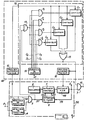
- a device for synchronizing a local clock signal with respect to a data signal comprising a servo device comprising a detector of the transitions of the data signal coupled to a phase comparator locating the position of the transitions with respect to the rising edge of the local clock signal, this signal being obtained from a generator comprising, in series, an oscillator, a divider whose value of the variable divider number is controlled by the signals obtained at the output of the comparator phase, and a fixed divider having an initialization input and which further comprises a fast synchronization circuit which preposition the fixed divider, is characterized in that this fast synchronization circuit (60) comprises counting means having an input signal coupled to the output of the transition detector, an output coupled to the initialization input of the fixed divider, and a counting control input coupled at the output of the fixed divider, these counting means counting the number of coincidences of n successive transitions received (n positive integer), each with k separate time intervals (
- a servo device 50 has an input terminal 1 intended to receive a signal modulated by the data of a message, and an output connected to a first input of an AND gate, 9.
- This device enslaved ment 50 comprises a carrier detector 3 coupling terminal 1 to a first input of an AND gate, 5, the second input of which is coupled to terminal 1, through a transition detector 4.
- the output of the AND gate, 5, is connected to a first input 31 of a phase comparator 6.
- the outputs 32 and 33 of this comparator 6 are respectively connected to the first and second control inputs of a variable divider 7, which has a third input connected to an oscillator 8, and an output connected to the first input of the AND gate, 9, through a fixed divider 90.
- the output of this divider 90 is also connected to a second input 35 of the phase comparator 6.
- the output of the AND gate, 9, is connected to the output terminal 11.
- a fast synchronization circuit 60 comprises counting means 70 composed of an AND gate, 13, of four AND gates, P i (i varying from 1 to 4), of four counters C i and d an OR gate, 15.
- the circuit 60 further comprises a first differentiator 12 coupling the output of the detector 3 to each of the reset inputs of the counters C i , a second differentiator 10 coupling an initialization input of the fixed divider 90 at the output of the OR gate, 15, which is connected to a second input of the AND gate, 9, and to a first input complemented by the AND gate, 13.
- the circuit 60 comprises a signal generator 14 having an input connected to the output of the fixed divider 90, and having four outputs S i .
- Each output Si is connected to a first input of the corresponding gate P i .
- Each of the second inputs of the doors P i is connected to the output of the AND gate, 13, the second input of which is connected to the output of the AND gate, 5.
- the output of each gate P i is connected to the i th input of the OR gate, 15, through the corresponding counter C i .
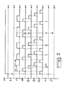
- signals a, b, c, d 1 , d 2 , d 3 , d 4 , e, f respectively present at the output of the carrier detector 3, at the output of the differentiator 12, at the output from the fixed divider 90, at the output S 1 , at the output S 2 , at the output S 3 and at the output S 4 of the decoder 14, at the output of the transition detector 4, and at the output of the differentiator 10.
- the signal a is a logic signal 1, characteristic of the presence of received signals, it opens, during its duration, the AND gate, 5, to the data transitions supplied by the transition detector 4 and represented by the signal e.
- the divider consisting of the variable divider 7 in series with the fixed divider 90 has a division rank, at rest, equal to 512, which can be increased to 511 or 513 under the action of signals respectively applied to the inputs 32 or 33 of the divider 7 (at the rate of once per period of the baud rate).
- the nominal frequency of oscillator 8 is, in this example, 614.4. kHz and that of the divider 90 output, at rest (signal c) of 1200 Hz, value of the clock pacing the data received.
- phase delay 3 ⁇ / 4, represented in FIG. 2, of the first transition detected e 1 with respect to the rising edge of the first period C 1 of the signal is measured by the phase comparator 6 which then assigns to the divider 7 the rank division 511, only once during the baud rate period.
- the rapid synchronization device 60 will speed up this process: the generator 14 delivers four periodic signals d 1 , d 2 , d3 and d 4 of the same frequency as the signal c but the duration of which is equal to a quarter of the period of this signal c, and each offset with respect to the next by ⁇ / 2, the rising edge of signal d 1 being set in phase with the rising edge of signal c.
- the gates P 1 to P 4 respectively allow the transitions of the signal e to pass only during the duration of the signals d 1 to d 4 and supply; in case of . coincidence, a logical 1 for characterizing the position of the transitions with respect to the rising edge of signal c. Given the uncertain nature of a single measurement, due to the effects of transmission noise, it is expected that four coincidences will be counted by one of the counters Co to C 4 to take account of the last coincidence.
- the counters Ci and C 4 of the counting means are reset to zero by a pulse obtained by differentiation of the rising edge of the output signal from the detector 3, which corresponds to the appearance of the carrier of the data signal on terminal 1. This differentiation is carried out by the differentiator 12:
- the invention is not limited to the mode of delivery sation described and shown.
- the signal generator 14 is such that it decomposes a period of the local clock signal into k time intervals of equal duration, with the correction step near T / q which affects the k th interval (T : desired local clock signal period).
- T desired local clock signal period
- control signals d i were obtained at the output of the signal generator 14, but it is within the reach of those skilled in the art to obtain these signals from the division rows of the divider 90.
Landscapes
- Engineering & Computer Science (AREA)
- Computer Networks & Wireless Communication (AREA)
- Signal Processing (AREA)
- Synchronisation In Digital Transmission Systems (AREA)
- Stabilization Of Oscillater, Synchronisation, Frequency Synthesizers (AREA)
Applications Claiming Priority (2)
| Application Number | Priority Date | Filing Date | Title |
|---|---|---|---|
| FR7914178 | 1979-06-01 | ||
| FR7914178A FR2458181A1 (fr) | 1979-06-01 | 1979-06-01 | Dispositif de synchronisation d'un signal d'horloge et systemes de transmission de donnees synchrones comportant un tel dispositif |
Publications (2)
| Publication Number | Publication Date |
|---|---|
| EP0020205A1 EP0020205A1 (fr) | 1980-12-10 |
| EP0020205B1 true EP0020205B1 (fr) | 1983-07-13 |
Family
ID=9226164
Family Applications (1)
| Application Number | Title | Priority Date | Filing Date |
|---|---|---|---|
| EP80400611A Expired EP0020205B1 (fr) | 1979-06-01 | 1980-05-06 | Dispositif de synchronisation d'un signal d'horloge et système de transmission de données synchrones comportant un tel dispositif |
Country Status (6)
| Country | Link |
|---|---|
| US (1) | US4352195A (show.php) |
| EP (1) | EP0020205B1 (show.php) |
| CA (1) | CA1153804A (show.php) |
| DE (1) | DE3064097D1 (show.php) |
| FR (1) | FR2458181A1 (show.php) |
| IL (1) | IL60181A (show.php) |
Families Citing this family (8)
| Publication number | Priority date | Publication date | Assignee | Title |
|---|---|---|---|---|
| FR2527031A1 (fr) * | 1982-05-17 | 1983-11-18 | Sintra Alcatel Sa | Circuit d'acquisition de l'horloge d'un message binaire code en nrz |
| US4604582A (en) * | 1985-01-04 | 1986-08-05 | Lockheed Electronics Company, Inc. | Digital phase correlator |
| JPH084262B2 (ja) * | 1986-03-31 | 1996-01-17 | 日本電気株式会社 | ビツト同期回路及び方法 |
| US4912734A (en) * | 1989-02-14 | 1990-03-27 | Ail Systems, Inc. | High resolution event occurrance time counter |
| US4979177A (en) * | 1989-10-26 | 1990-12-18 | Tektronix, Inc. | Enhanced counter/timer resolution in a logic analyzer |
| FR2781943B1 (fr) * | 1998-07-30 | 2000-09-15 | Thomson Multimedia Sa | Procede de recuperation d'horloge lors de l'echantillonnage de signaux de type numerique |
| DE10018190C2 (de) * | 1999-05-18 | 2003-04-17 | Ibm | Unterbrechnungsloses Umschalten zwischen zwei Oszillator-Präzisionstaktgebern |
| US11455002B1 (en) * | 2021-05-27 | 2022-09-27 | Cirrus Logic, Inc. | Timing signal synchronisation |
Family Cites Families (7)
| Publication number | Priority date | Publication date | Assignee | Title |
|---|---|---|---|---|
| FR1422959A (fr) * | 1964-11-13 | 1966-01-03 | Thomson Houston Comp Francaise | Perfectionnements aux dispositifs d'asservissement en phase |
| US3440547A (en) * | 1966-04-11 | 1969-04-22 | Bell Telephone Labor Inc | Synchronizer for modifying the advance of timing wave countdown circuits |
| US3562661A (en) * | 1969-01-15 | 1971-02-09 | Ibm | Digital automatic phase and frequency control system |
| US3755748A (en) * | 1972-03-06 | 1973-08-28 | Motorola Inc | Digital phase shifter/synchronizer and method of shifting |
| FR2301964A1 (fr) * | 1975-02-21 | 1976-09-17 | Telecommunications Sa | Horloge numerique synchronisee |
| CA1057860A (en) * | 1976-01-08 | 1979-07-03 | Sperry Rand Corporation | Two mode harmonic and nonharmonic phase detector |
| US4229822A (en) * | 1977-09-06 | 1980-10-21 | Motorola, Inc. | Data detector for a data communication system |
-
1979
- 1979-06-01 FR FR7914178A patent/FR2458181A1/fr active Granted
-
1980
- 1980-05-06 DE DE8080400611T patent/DE3064097D1/de not_active Expired
- 1980-05-06 EP EP80400611A patent/EP0020205B1/fr not_active Expired
- 1980-05-28 IL IL60181A patent/IL60181A/xx unknown
- 1980-05-29 CA CA000352979A patent/CA1153804A/en not_active Expired
- 1980-05-30 US US06/154,955 patent/US4352195A/en not_active Expired - Lifetime
Also Published As
| Publication number | Publication date |
|---|---|
| CA1153804A (en) | 1983-09-13 |
| DE3064097D1 (en) | 1983-08-18 |
| IL60181A (en) | 1982-11-30 |
| IL60181A0 (en) | 1980-07-31 |
| EP0020205A1 (fr) | 1980-12-10 |
| FR2458181A1 (fr) | 1980-12-26 |
| FR2458181B1 (show.php) | 1985-04-05 |
| US4352195A (en) | 1982-09-28 |
Similar Documents
| Publication | Publication Date | Title |
|---|---|---|
| EP0015014B1 (fr) | Dispositif de resynchronisation rapide d'une horloge | |
| EP0190730A1 (fr) | Dispositif de distribution d'horloge tripliquée, chaque signal d'horloge comportant un signal de synchronisation | |
| EP0020205B1 (fr) | Dispositif de synchronisation d'un signal d'horloge et système de transmission de données synchrones comportant un tel dispositif | |
| FR2473824A1 (fr) | Procede de commutation entre les recepteurs et les correlateurs d'un systeme de communication et appareil de reception-correlation pour la mise en oeuvre de ce procede | |
| EP0716501B1 (fr) | Comparateur de phase entre un signal numérique et un signal d'horloge, et boucle à verrouillage de phase correspondante | |
| EP0049652B1 (fr) | Dispositif de compression et dispositif de décompression temporelle de données | |
| FR2478398A1 (fr) | Controle numerique de la vitesse d'un moteur | |
| EP0037299B1 (fr) | Dispositif de synchronisation d'informations numériques transmises par paquets | |
| FR2598570A1 (fr) | Circuit retardateur numerique | |
| EP3617820B1 (fr) | Procédé et système de synchronisation | |
| EP0302562B1 (fr) | Synthétiseur de fréquences présentant un dispositif indicateur d'accord | |
| EP0056208B1 (fr) | Procédé et dispositif de synchronisation de messages | |
| EP0526359B1 (fr) | Procédé et dispositif de synchronisation d'un signal | |
| EP0193453B1 (fr) | Dispositif pour contrôler la période séparant des impulsions | |
| EP0051531B1 (fr) | Appareillage pour la datation précise d'un évènement par rapport à une référence de temps | |
| EP0244316B1 (fr) | Dispositif de décodage pour code CMI | |
| EP0541431B1 (fr) | Méthode et dispositif pour restituer un signal d'horloge rythmant la transmission de signaux reçus | |
| EP0399023B1 (fr) | Dispositif de synchronisation pour une suite de trames a longueur variable | |
| FR2478410A1 (fr) | Procede et dispositif de synchronisation d'un signal de donnees binaires | |
| FR2526247A1 (fr) | Dispositif de synchronisation bit pour modulateur-demodulateur ou recepteur de transmission de donnees | |
| EP0016678B1 (fr) | Dispositif de reconstitution d'horloge | |
| EP1127305A1 (fr) | Procede et dispositif de synchronisation d'une horloge locale sur l'horloge d'un reseau de communication sans fil | |
| FR2535554A1 (fr) | Procede et appareil pour la reception de messages radio a signaux de type biphase | |
| FR2545304A1 (fr) | Dispositif d'extraction des impulsions de synchronisation d'un signal video et de generation de signaux d'alignement | |
| EP0027081A1 (fr) | Equipement de mesure de distance de type DME |
Legal Events
| Date | Code | Title | Description |
|---|---|---|---|
| PUAI | Public reference made under article 153(3) epc to a published international application that has entered the european phase |
Free format text: ORIGINAL CODE: 0009012 |
|
| AK | Designated contracting states |
Designated state(s): DE GB IT NL SE |
|
| 17P | Request for examination filed |
Effective date: 19810508 |
|
| ITF | It: translation for a ep patent filed | ||
| GRAA | (expected) grant |
Free format text: ORIGINAL CODE: 0009210 |
|
| AK | Designated contracting states |
Designated state(s): DE GB IT NL SE |
|
| REF | Corresponds to: |
Ref document number: 3064097 Country of ref document: DE Date of ref document: 19830818 |
|
| PLBE | No opposition filed within time limit |
Free format text: ORIGINAL CODE: 0009261 |
|
| STAA | Information on the status of an ep patent application or granted ep patent |
Free format text: STATUS: NO OPPOSITION FILED WITHIN TIME LIMIT |
|
| 26N | No opposition filed | ||
| PGFP | Annual fee paid to national office [announced via postgrant information from national office to epo] |
Ref country code: GB Payment date: 19920424 Year of fee payment: 13 |
|
| PGFP | Annual fee paid to national office [announced via postgrant information from national office to epo] |
Ref country code: SE Payment date: 19920522 Year of fee payment: 13 |
|
| ITTA | It: last paid annual fee | ||
| PGFP | Annual fee paid to national office [announced via postgrant information from national office to epo] |
Ref country code: NL Payment date: 19920531 Year of fee payment: 13 |
|
| PGFP | Annual fee paid to national office [announced via postgrant information from national office to epo] |
Ref country code: DE Payment date: 19920615 Year of fee payment: 13 |
|
| PG25 | Lapsed in a contracting state [announced via postgrant information from national office to epo] |
Ref country code: GB Effective date: 19930506 |
|
| PG25 | Lapsed in a contracting state [announced via postgrant information from national office to epo] |
Ref country code: SE Effective date: 19930507 |
|
| PG25 | Lapsed in a contracting state [announced via postgrant information from national office to epo] |
Ref country code: NL Effective date: 19931201 |
|
| GBPC | Gb: european patent ceased through non-payment of renewal fee |
Effective date: 19930506 |
|
| NLV4 | Nl: lapsed or anulled due to non-payment of the annual fee | ||
| PG25 | Lapsed in a contracting state [announced via postgrant information from national office to epo] |
Ref country code: DE Effective date: 19940201 |
|
| EUG | Se: european patent has lapsed |
Ref document number: 80400611.2 Effective date: 19931210 |