EP0017584A1 - Procédé et système d'exploitation d'une mémoire adressable permettant d'associer à volonté des qualificatifs aux données contenues dans la mémoire - Google Patents
Procédé et système d'exploitation d'une mémoire adressable permettant d'associer à volonté des qualificatifs aux données contenues dans la mémoire Download PDFInfo
- Publication number
- EP0017584A1 EP0017584A1 EP80400439A EP80400439A EP0017584A1 EP 0017584 A1 EP0017584 A1 EP 0017584A1 EP 80400439 A EP80400439 A EP 80400439A EP 80400439 A EP80400439 A EP 80400439A EP 0017584 A1 EP0017584 A1 EP 0017584A1
- Authority
- EP
- European Patent Office
- Prior art keywords
- data
- memory
- qualifier
- qualifiers
- circuits
- Prior art date
- Legal status (The legal status is an assumption and is not a legal conclusion. Google has not performed a legal analysis and makes no representation as to the accuracy of the status listed.)
- Withdrawn
Links
Images



Classifications
-
- G—PHYSICS
- G06—COMPUTING OR CALCULATING; COUNTING
- G06F—ELECTRIC DIGITAL DATA PROCESSING
- G06F12/00—Accessing, addressing or allocating within memory systems or architectures
- G06F12/02—Addressing or allocation; Relocation
- G06F12/06—Addressing a physical block of locations, e.g. base addressing, module addressing, memory dedication
- G06F12/0638—Combination of memories, e.g. ROM and RAM such as to permit replacement or supplementing of words in one module by words in another module
-
- G—PHYSICS
- G06—COMPUTING OR CALCULATING; COUNTING
- G06F—ELECTRIC DIGITAL DATA PROCESSING
- G06F12/00—Accessing, addressing or allocating within memory systems or architectures
- G06F12/02—Addressing or allocation; Relocation
- G06F12/04—Addressing variable-length words or parts of words
Definitions
- the invention relates to addressable data storage devices used in data processing systems and essentially relates to a method and an operating system by user means of an addressable memory making it possible to qualify the data of the memory by association of data qualifiers.
- the system according to the invention advantageously makes it possible, during the testing of development or troubleshooting of a data processing system using an addressable memory, to associate with the data qualifiers characteristics of the data or characteristics of the processing undergone by the data. . These qualifiers allow the user devices to know at any time a particular character of the data.
- This invention is particularly applicable to data processing systems using microprocessors and in which it is necessary to carry out control and test operations on the data as is the case during periods of development and maintenance.
- the processing unit draws data as and when it is needed from a data memory. In particular, this is where she picks up instructions for the running program.
- the various instructions constituting the program being developed or tested are checked and tested. For example, to be certain at the end of the operation of the completeness of the tests carried out, it is necessary to ensure that all the instructions have been checked and tested. There is currently no simple way to achieve this certainty.
- One of the possible means is the recording in a memory of all the addresses called. This method requires additional memory locations and laborious processing because the consecutive instructions are not necessarily located at addresses that are also consecutive, it is necessary to perform a pre-sorting before carrying out the check.
- the invention provides a method and a device consisting in! associate with each data contained in the data memory a qualifier controlled by the processing unit and whose role is to enable the unit processing to know at will the characteristic of a data by reading this associated qualifier.
- the subject of the invention is a method for using by user means data contained in an addressable memory of the type consisting in associating qualifiers with said data contained in said addressable memory and in using said addressable memory by, in particular, calling of said user means, said data characterized in that said qualification associated with the data comprises the writing of qualifiers in qualification means associated with said data, said qualifiers coming from said user means, and in that said use of addressable memory comprises the control of said qualification means each time a datum is called to generate information relating to said qualifier associated with said called datum and to transmit this said information to said user means.
- said qualifiers have different configurations, which said different configurations are defined by the user means.
- the aforementioned qualification comprises an intermediate step before said writing in said qualification means, in this said intermediate step said user means transmit said qualifier to intermediate means which in turn transmit said qualifier for writing in said qualification means and said use of said addressable memory includes stimulation of the intermediate means for the transmission to said user means of said information relating to said qualifier.
- said transmission of said information relating to said qualifier comprises a first phase of notification to the user means of the presence of the qualifier in said qualification means and a second phase in which said qualifier is transmitted in turn. at the request of said user means who were alerted during said first phase.
- This operating system is characterized in that it includes means for qualifying said data contained in said addressable data memory for qualifying said data on instruction from said processing means by writing a qualifier in locations associated with the addresses containing said data, which associated locations respond to calls from said particular addresses by said processing circuits by sending information relating to said qualifiers to said processing circuits.
- the invention also relates to an operating system characterized in that it comprises intermediate means placed between said processing circuits and said qualification means for controlling the exchange of said information relating to said qualifiers between said processing circuits and said qualification means to allow said processing circuits to differ the use of qualifiers and indicators.
- said intermediate means have a control means for making known to said processing circuits that they have just called up one of said data comprising an associated qualifier.
- said associated locations are contained in a memory of the qualifiers which is a memory similar to said data memory, the addressing of which is ensured by said addressing circuits of said means of use.
- said intermediate device consists of an addressable device of the type used to connect said processing means with peripheral devices with which they exchange data.
- the invention is of course aimed at integrated circuit boards, modules or the like equipped with a logic system meeting the preceding characteristics.
- FIG. 1 represents the flow diagram of the operations which take place in a data processing system using said method.
- this flowchart relates to the operation of a data processing system comprising, inter alia, a microprocessor and associated circuits as they are described, for example, in the document published by the company "MOTOROLA” in February 1976, referenced 9701-5 (IMPERIAL LITHO B 55769) and entitled M6800 MICROCOMPUTER SYSTEM DESIGN DATA.
- the microprocessor must obtain instructions contained in an addressable memory which will be called data memory.
- the address of the instructions to be obtained is contained in an ordinal counter or instruction counter. This address is communicated to the addressable memory which in return, on request of a read cycle, will transmit the content of the address thus called.
- the instructions thus collected are placed in an instruction register.
- the microprocessor can store instructions or data in the addressable memory by calling the storage address, transmitting the instructions or data to be recorded and requesting a cycle of writing or writing in memory.
- the microprocessor controls the progress of the ordinal counter: the content of the counter is then the address of the next instruction.
- the block (1) represents the operation of defining the address of the next instruction.
- the system acquires the instruction contained at this address. This acquisition is represented by block (2).
- This operation is followed by the operation of decoding of the instruction which is represented by the block (3).
- This decoding allows the system to know the nature of the operations defined by the instruction. It is thus possible to know whether these operations require a cycle of the data memory. If the statement does not appeal to memory, it is executed (5) and on completion the order is given 'the program to move to the next instruction by an execution end signal applied input 3 of the block (1).
- the instruction uses memory, it is examined in (6) whether the requested memory cycle is a read cycle or a write cycle.
- the system determines in (7) whether the called address must be assigned a qualifier associated with the data contained at this address. If so, the system acquires in (8) the configuration of the associated qualifier. Then, the system acquires in (9) the data to be stored in the memory. Finally, in (10) the system performs on the one hand the loading of the associated qualifier in the memory of the qualifiers, on the other hand, the loading of the data in the data memory. These two loading operations being finished, the system stimulates by the input 1 of the block (1) the progression of the program.
- the system performs in (11) the acquisition of the data to be stored, in (12) it performs the loading of the data in the memory data then restart the program progress via terminal 1 of block (1).
- this qualifier is examined in (15). This qualifier characterizes the address read and the microprocessor performs the corresponding processing in (16). The end of this processing restarts by the input (1) of the block (1) the program sequence.
- the data memory contains data qualified by qualifiers.
- This qualification is obtained in writing by associating with the addresses concerned an associated qualifier. When reading an address containing qualified data, calling this address shows the qualifier associated with the data contained at this address.
- This qualifier provides the system with information regarding the data with which the qualifier is associated. This. qualifier can contain, for example, the indication of a processing carried out on this data.
- the data processing circuits (18) are connected by a link (19) to the addressing circuits (21), by a link (20) to the input-output buffer register (22), by a link (27) to the qualification means (25) and by a link (29) to the data memory (24) and to the qualification means (25).
- the link (27) is the qualifiers omnibus and the link (29) is the control omnibus.
- the output of the addressing circuits (21) supplies the addressing omnibus (23).
- the output of the buffer register (22) feeds the data bus (26).
- the addressing omnibus (23) is connected to the data memory (24) and to the qualification means (25).
- the data memory (24) therefore has three inputs attacked respectively by the address omnibus (23), the control omnibus (29) and the data omnibus (26).
- the qualification means (25) also have 3 inputs attacked respectively by the omnibus (23) of the addresses, the control omnibus (29) and the qualifier omnibus (27).
- the processing circuits (18) want to exchange data with the data memories (24) and a qualifier with the qualification means (25), they place the address of the location, where the data and the qualifier are located. aforementioned, on the link (19) which supplies the addressing circuit (19), the latter supply the addressing omnibus (23) which on the one hand addresses a location in the memory (24) of the data and d 'other hand, address a location in the qualification means (25), we see that the address of two locations is the same address in these two devices. It is sufficient for the qualification means to have a space available for each of the data items to be qualified in order to register the corresponding qualifier.
- the processing circuits (18) place on the control omnibus (29) the signals defining the nature of the operating cycle requested from the memories (24) and (25). If the processing circuits (18) wish to obtain a write cycle, before starting this write cycle, on the one hand, place the data to be stored on the link (20) which loads the buffer register ( 22) data and on the other hand, if it is a data to be qualified, place the qualifier corresponding to this address on the omnibus (27) of the qualifiers. Once these operations have been completed, the processing circuits (18) initiate the write cycle which respectively introduces the data placed on the data omnibus (26) into the data memory (24) and the qualifier placed on the data omnibus (27). qualifiers in the means - (25) of qualification.
- the processing circuits (18) can, during a writing cycle, load data into memory (24) and, if this data is to be qualified, load the means (25) of qualification with the qualifier corresponding to this data. This qualifier will be called subsequently the qualifier associated with the qualified address.
- the processing circuits (18) command a read cycle.
- the processing circuits (18) then initiate a read cycle.
- This reading cycle places data, therefore on the data omnibus (26), at the output of the memory (24), therefore the data which is contained in the addressed location.
- the data omnibus (26) transmits this read data to the input-output buffer register (22) which in turn, through the link (20), transmits this data to the processing circuit (18).
- a reading cycle was also carried out in the qualification means (25). If in the address space, which is therefore at an address associated with that of the data, there is a qualifier, which proves that it is an address containing a qualified data, this qualifier is placed at the output of the qualification means (25) and at the same time, transmitted by the omnibus (27) to the processing circuits (18). If the reading of this address of the qualification means (25) does not provide a qualifier, this means that this address does not contain qualified data and no signal is supplied to the qualifiers omnibus (27).
- FIG. 3 is shown a variant of the system shown in FIG. 2.
- intermediate means (30) have been interposed between the user means (28) and the qualification means (25).
- the transmission of the qualifiers no longer takes place directly through an omnibus (27) of the qualifiers.
- the qualification means (25) are connected to the address omnibus (23), to the control omnibus (29) and to the deferred qualifier omnibus (31).
- the deferred qualifier bus (31) is connected at its other end to the intermediate means (30).
- These intermediate means (30) also receive the address bus (23) and the data bus (26).
- the user devices (28) want to write data in the data memory (24) by associating with this data to write a qualifier, they proceed as follows. They place, on the omnibus (23) of addresses, the address of the intermediate means (30), they place on the omnibus (26) data the qualifier associates with the data to be written to the associated address and on the 'omnibus (29) controls the order to execute a write cycle. This set of signals applied to the intermediate means (30) will cause the qualifier to be introduced into the intermediate means (30).
- the means (28) users place the address of the data to be written in memory (24) of the data on the address omnibus (23), the data to be written in memory (24) of the data on the omnibus (26) data, the order to execute a write cycle on the omnibus (29) of control.
- This set of signals applied to the memory (24) of the data and to the qualification means (25) will cause these 2 organs (24) and (25) to execute a write cycle.
- this write cycle will store the data placed on the omnibus (26) of the data in the location of the memory (24) of the data defined by the address placed on the omnibus (23). addresses.
- this write cycle command will place the qualifier received previously on the omnibus (31) of the deferred qualifiers.
- this writing cycle causes the storage of the qualifier placed on the omnibus (31) of the qualifiers deferred in the location of the means (25) of qualification defined by the address placed on the omnibus. (23) addresses.
- the means (28) users want to read the contents of a location in the data memory (24), they place addresses on the highway (23), the address of the location to be read and on the highway ( 29) control they command a reading cycle.
- the arrival of the signals carried by these 2 omnibuses on the data memory (24) triggers the execution of the read cycle of the data memory (24).
- This read cycle places the data contained in the location designated by the address placed on the omnibus (23) of the addresses on the omnibus (26) of the data.
- the qualification means (25) receive addresses, the address of the location read in the data memory by the omnibus (23) and by the omnibus (29) a read command and execute a reading cycle of the content of the means location (25) having the same address as that called in the memory (24) of the data. If there is a qualifier stored in this location, the read cycle places this qualifier on the omnibus (31) of the deferred qualifiers. This omnibus (31) of the deferred qualifiers transmits this qualifier to the intermediate means (30).
- the operating means (28) request, by an appropriate command placed on the control omnibus (29), the intermediate means (30) to place on the omnibus ( 26) data the result of the reading carried out at the address called in the qualification means (25). If there is no associated qualifier, no signal will be transmitted on the data bus (26). If there is an associated qualifier, that qualifier will be placed on the data bus (26).
- the means (25) of qualification after an operation of reading the content of a location defined by an address warn the means (28) users in the event of detection of the presence of a qualifier associated with the data contained at the called address. For this, they place on the control omnibus (29) a signal informing the user means (28) of the existence of a qualifier associated with the data called.
- This information of the means (28) users of the existence of this qualifier avoids having to request a special cycle from the intermediate means (30).
- the qualification means (25) consist of a memory analogous to the data memory (24). This memory is called the qualifier memory (25) because of its resemblance to the data memory (24).
- the intermediate means (30) consist of an addressable device similar to those used to connect the user means (28) of data with peripheral means: the intermediate means (30) are considered by the user means (28) as a particular peripheral means.
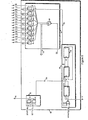
- FIG. 4 represents a preferred embodiment of the invention produced around a MOTOROLA MC 6800 microprocessor.
- the means (28) of use consist of a clock (49) of the MOTOROLA MC 6871 type and of a microprocessor (48) of the MOTOROLA MC 6800 type.
- the clock (49) MC 6871 produces two synchronization signals which define the operating phases of the entire system. These two signals are respectively called 1 and ⁇ 2. These signals are transmitted to the microprocessor (48).
- the data memory (24) consists of 8 MOTOROLA integrated circuits of the MCM 6605A type. These circuits are represented in (50), (51), (52), (53), (54), (55), (56), (57). Each of these integrated circuits is an addressable memory comprising 4096 locations with a capacity of 1 bit.
- the circuit (50) stores the bits O of the data
- the circuit (51) stores the bit 1 so on to the integrated circuit (57) which stores the bit 7.
- the memory (25) of the qualifiers is analogous to the memory (24) of the data.
- the integrated circuit (60) stores the bits O of the qualifiers so on until the integrated circuit (67) which stores the bit 7 of the qualifiers.
- the memory (24) of the data exchanges the data which it stores with the microprocessor through the data bus (26): the circuit (50) exchanges the bit 0 by the wire D O , the circuit (51) exchanges the bit 1 by wire D l , and so on up to the circuit (57) which does so by wire D7.
- the memory (25) of the qualifiers exchanges the qualification bits with the microprocessor (48) through the intermediate means (30) which play, in some way so, a relay role.
- These intermediate means (30) comprise a unifier.
- the interface adapter (70) is a MOTOROLA integrated circuit of type MC 6820. This circuit can support the connection of 2 peripherals. In the system shown in FIG. 4, only one of these 2 connection possibilities is used. The connection possibility used is sometimes used in read mode and sometimes in write mode according to the microprocessor commands. Of course, it is perfectly possible to use the 2 connection possibilities and in this case each of the connection possibilities is reserved for an operating mode: one of the possibilities is reserved for writing mode, the other possibility is reserved for reading mode .
- the central part is the network (102) of storage cells.
- the cell to be reached for reading or writing is addressed on the one hand by the column decoder (100) and on the other hand by the row decoder (101).
- the column decoder (100) is supplied by the wires A 0 , A 1 , A 2 , A 3 , A 4 of the address bus (23).
- the line decoder (101) is supplied by wires A5 to A 15 of the address omnibus (23).
- In (107) is represented the internal clock ce of the integrated circuit (60). This internal clock (107) receives on its input (1) the initialization signal "INITIALISAT", on its input (2) the signal "WRITE" and on its input (3) the clock signal "# 2 ".
- the outputs of this internal clock (107) are: in (4) the clock signal “ ⁇ 1 " and in (6) the clock signal "43". These three clock signals “ ⁇ 1 ", “# 2 " and “# 3 " feed the network (102) of the memory cells to control the operating phases of these said memory cells.
- In (103) are represented the data input-output circuits of the memory. These input-output circuits (103) receive on their input (1) the value of the bit to be recorded in the case of a write cycle or the value of the bit to be recorded in the case of a refresh cycle. The output (2) of the input-output circuit (103) transmits the value of the bit read at the location selected by the address in the case of a read cycle in the case of a refresh cycle.
- the terminal (3) of the circuit (105) is connected to the network (102) of the storage cells.
- this terminal (3) of the input-output circuit (103) will send the value of the bit to be recorded to the network (102) of storage cells. or re-record.
- this terminal (3) will receive from the network (102) of storage cells the value of the bit contained in the cell selected by the decoders (100) and (101).
- the terminal (1) of the input-output circuit (103) is supplied by the output (4) of the conditioner (109).
- This conditioner (109) receives on its terminal (1) the clock signal " ⁇ 3 " coming from the internal clock (107), on its terminal (2) a signal emitted by the output (3) of the circuit (108 ) OU-EXCLUSIVE and on its terminal (3) a selection signal emitted by the qualifier writing controller (69).
- the OR-EXCLUSIVE circuit (108) receives on its input (1) the value of the bit to be stored, in the case of a write, sent by the write controller (69) of the qualifiers.
- the terminal (2) of the input-output circuit (103) supplies the input of the OR-EXCLUSIVE circuit (104).
- This OU-EXCLUSIVE circuit (104) receives on its input (2) a signal emitted by the internal clock (107).
- the output (3) of this circuit (104) supplies the input (1) of the controlled amplifier (105).
- This amplifier (105) controlled receives on its control input (2) a signal emitted by the conditioner (123) and its output (3) sends, in the case of a read cycle, the value of the bit read towards the controller ( 69) writing qualifiers.
- the conditioner (123) receives on its input (1) the clock signal ⁇ 2 and on its input (2) a selection signal emitted by the qualifier writing controller (69).
- the integrated circuit (70) referenced MOTOROLA 6820 is provided by the manufacturer for the connection of 2 peripherals to the buses (23), (26) and (29). In the embodiment described in this example, only one of these connection possibilities is used. In the figures are shown only the functional assemblies called into question by the invention. There are five of these sets.
- a multiple link (146) connects the terminal (5) of the function control block (135) and the multiple terminal (3) of the transfer control block (138).
- An omnibus (147) connects the multiple terminal (2) of the upstream buffer register (136) and the multiple terminal (1) of the transfer control block (138).
- An omnibus (151) connects the multiple terminal (4) of the transfer control block (138) and the multiple terminal (2) of the downstream buffer register (139).
- a multi-wire link (149) connects the multi-wire terminal (2) of the transfer control block (138) and the multi-wire terminal (3) of the interrupt control block (137).
- the transfer control block (135) further comprises 4 terminals including 1 multiple terminal.
- the INITIALISAT initialization line arrives at terminal (1).
- On the terminal (2) arrives the clock distribution line 1 2 .
- On the terminal (3) comes the WRITE write command line.
- On the multi-wire terminal (4) arrive 4 lines of the bus (23) with addresses A 0, Al, A ll , A 15 and a validation line SELECTION.
- the upstream buffer register (136) receives on its multi-wire terminal (1) 8 lines Do, ..., D 7 upstream of the bus (26) data.
- the interrupt control block (137) receives on its terminal (1) an INTERRUPT interrupt request line, on its terminal (2) a line (131) connected to the bistable (124) input (+) of the writing unifier (69) and on its terminal (3) a link (150) connected to the output (2) of the mixer (153) of the writing unifier.
- the buffer register (139) receives on its multi-wire terminal (1) an omnibus (152) connected to the terminal (1) of the mixer (153) and to the terminals (2) of the different conditioners (182 to 189) according to a distribution which will be defined below.
- the write unifier (69) is also shown in FIG. 6.
- the block (90) is the block for controlling the uniqueness of writing
- the block (91) is the block for controlling the exchanges between the memory (25) of the qualifiers and the interface adapter (70)
- the block (92) is the block for controlling the operations for writing to the memory (25) of the qualifiers.
- the bistables are represented with the following convention: the two signal inputs are indicated by the signs (+) and (-) and the outputs by the signs (1) and (0).
- the bistable has a clock input indicated by the letter (H).
- the writing uniqueness control block (90) includes the mixer (123), the bistable (124), the bistable (126) and the bistable (128).
- the terminal (1) of the mixer (123) receives the line (130) upstream of the output (1) of the bistable (126) and the terminal (2) receives the INITIALIS initialization line upstream of the control omnibus (29).
- the outlet (3) of the mixer (123) is connected to the inlet (-) of the bistable (124).
- the input (+) of the bistable (124) is connected to the link (131).
- the output (1) of the bistable (124) is connected to the input (+) of the bistable (126).
- the output (0) of the bistable (124) feeds the line (205) which leads to the input (1) of the conditioners (201) of the circuits (60 to 67) integrated in the memory (25) of the qualifiers.
- the input (-) of the bistable (126) is connected to the output (1) of the bistable (128).
- the output (1) of the bistable (126) is connected to the input (+) of the bistable (128) and the output (0) of the bistable (126) is connected to the input (-) of the bistable (128).
- the bistables (124) and (128) receive on their input H the clock signal 0 2 and the bistable (126) receives on their input H the clock signal ⁇ pi.
- the block (92) for controlling write operations is composed of a conditioner (200) and a conditioner (201) with inverted output.
- the conditioner (201) with inverted output receives on its input (1) the write command line "WRITE" and on its input (2) the line (205) which emanates from the output (0) of the bistable (124) .
- the output of this conditioner is connected to the input (2) of the conditioner (200) which receives on its input (1) the SELECTION validation line.
- the output (3) of this conditioner feeds the line (115) which leads to the input (3) of the conditioner (109).
- the exchange control block (91) includes a mixer (153) and eight conditioners (182 to 189).
- the bus (152) which emanates from the downstream buffer register (139) is connected to the mixer (153) and the conditioners (182 to 189) as follows: the omnibus (152) comprises 8 lines corresponding through the interface adapter (70) to the 8 lines of the data omnibus (26).
- the terminal (1) of the mixer (153) includes 8 inputs each connected to a different line from the bus (142).
- the conditioners (182 to 189) the input (2) of each conditioner is connected to a different line: the conditioner (182) to the line corresponding to D 0 , ... the conditioner (189) to the line corresponding to D 7 .
- Each of the lines is extended respectively to the integrated circuit corresponding to the bit concerned: the line (167) to the circuit (60), the line (169) to the circuit (61), the line (171) to the circuit (62) , the line (173) to the circuit (63), the line (175) to the circuit (63), the line (175) to the circuit (64), the line (177) to the circuit (65), the line (179) to the circuit (66) and the line (181) to the circuit (67).
- the outputs (3) of the conditioners (182 to 189) are respectively connected to the integrated circuit corresponding to the bit concerned: the line (166) to the circuit (60), the line (168) to the circuit (61), the line (170) to circuit (62), line (172) to circuit (63), line (174) to circuit (64), line (176) to circuit (65), line (178) to circuit (66) and the line (180) to the circuit (67).
- the write unification controller (69) is initialized by applying an INITIALIS signal to the input (2) of the mixer (123). This signal passes through the mixer (123) to enter via the terminal (-) of the bistable (124) which is synchronized by the clock signal% 2 . The bistable (124) will therefore see its output (1) switch to zero on the falling edge of the clock signal ⁇ 2 . The initialization has no effect on the bistables (126) and (128) because these two bistables initialize each other.
- the microprocessor (48) When the microprocessor (48) wants to load a qualifier into the memory (25) of the qualifiers, it must carry out two operations. First, it must load the qualifier into the interface adaptation circuit (70). Then, it must command a write cycle in the data memory (24). This write cycle must be performed at the address containing the data to be qualified. The execution of this write cycle in the memory (24) of the data leads to the parallel execution of a write cycle in the memory (25) of the qualifiers. During this parallel writing cycle, the qualifier which was stored in the interface adaptation circuit (70) is stored in the associated address of the memory (25) of the qualifiers.
- the function control block (135) having recognized its address on its multiple terminal (4) and receiving a write order on its terminal (3), places the commands to be transmitted to the block (138) on its multiple terminal (5) ) transfer control. These commands are transmitted through the multi-wire link (146) to the terminal (3) of the transfer control block (138).
- the transfer control block (138) organizes the internal circuits of the interface adaptation circuit (70) so that the content of the upstream buffer register (136) is transmitted to the downstream buffer register (139). through the multi-wire link (147), then through the transfer control block (138) and finally through the multi-wire link (151). In this way, the configuration of the qualifier D O to D 7 which has been placed on the data bus (26) is contained in the register (139) downstream buffer.
- This downstream buffer register (139) transmits on its multiple terminal (1) and from there, through the multi-wire link (152), the configuration Do to D 7 from the qualifier to the write unification controller (69). Furthermore, the transfer control block (138) informs the switch control block (137) of the correct execution of the transfer of the qualifier in the downstream buffer register (139). For this, the transfer control block (138) places a signal for successful execution of the transfer on its terminal (2), this signal through the link (149) enters the terminal (3) of the block (137) for controlling the transfer. interruptions. In response to this signal, the interrupt control block (137) transmits, from its terminal (2) and through the link (131), to the write unification controller (69) a signal informing the latter that the configuration of the qualifier is available on the link (152). In summary, the interface adaptation circuit (70) placed the configuration of the qualifier on the link (152) and informed the link unification controller (69) by the link (131).
- the block (137) for controlling interruptions informs the write unification controller (69) by sending a signal on the link (131) which arrives at the terminal (+ ) the bistable (124) which is in the block (90) for checking the uniqueness of writing. Under the action of this stress, the bistable (124) switches and its output (1) goes high on the falling edge of the clock signal ⁇ 2 .
- This high level means for the write uniqueness control block (90) that the configuration of the qualifier is available at the output of the interface adaptation circuit (70) on the bus (152).
- the output (1) of the bistable (124) is connected to the input (+) of the bistable (126): the bistable (126) therefore switches and its output (1) will go to a high level on the falling edge of the 'clock ⁇ 1 .
- the output (1) of the bistable (126) is connected to the line (130).
- This line (130) when it is high allows the passage of the configuration contained in the bus (152) through the series of conditioners (182, 183, 184, 185, 186, 187, 188, 189) which control the passage to the lines (166, 168, 170, 172, 174, 176, 178, 180) for entering the bits in the circuits (60, 61, 62, 63, 64, 65, 66, 67).
- bistable (126) has its input (+) connected to the output (1) of the bistable (126): switching to a high level of this output switches the bistable (128) whose output (1) changes to a level high on the falling edge of the clock signal ⁇ 2 .
- This high output means that the configuration of the qualifier can be written.
- the output (1) of bistable (128) enters the input (-) of the bistable (126) whose output (1) goes to a low level on the falling edge of the clock signal 1.
- the output (0) of the bistable (126) has gone to a high level and transmits this level to the input (-) of the bistable (128) which switches: its output (1) goes to a low level.
- the block (90) for checking the uniqueness of the writing has been brought back to its initial state.
- the output (1) of the bistable (126), which controls the line (130), being at a low level closes the conditioners (182 to 189) of the block (91) for controlling exchanges between the memory (25) of the qualifiers and the interface matching circuit (70). Closing these conditioners therefore isolates the memory (25) of the interface adaptation circuit (70) qualifiers.
- the conditioners were only opened during the duration of a write cycle as will be clearly seen in FIG. 7 which illustrates the timing diagram of the signals involved during a write cycle in memory (25) of the qualifiers.
- the block (92) for controlling write operations receives from the block (90) for controlling the uniqueness of writing a line (205) which emanates from the terminal (0) of the bistable (124) and which leads to the input (2) of the conditioner (201) with reverse output.
- the output (1) of the bistable (124) is at a low value, which means that there is no qualifier configuration available in the interface adapter circuit (70)
- the output (0) of this bistable is at a high value.
- the input (2) of the conditioner (201) receives a positive signal. If a WRITE write command is sent by the microprocessor (48) to the input (1) of the conditioner (201), the output (3) of the latter is low since the 2 input conditions are satisfied.
- the output (3) of the conditioner (201) retransmits the low level to the input (2) of the conditioner (200) which consequently is closed.
- the conditioner (200) being closed the SELECTION validation signal is not transmitted to the output (3) of this conditioner and therefore is not transmitted on the line (115) which controls the conditioners (109) and (123) from the memory (25) of the qualifiers.
- the absence of the SELECTION signal in the presence of a WRITE command causes the execution of a refresh cycle of the content of the address called.
- the block (92) for controlling the write operations receives on the line (205) a low level signal which signifies that a configuration of a qualifier is available at the output of the circuit (70) of interface adaptation
- the output (3) of the conditioner (201) is a high value since its input (2) is at a low value.
- the conditioner (200) is therefore open and the SELECTION validation signal crosses it to supply the line (115).
- the line (115) being at a high level, the memory (25) of the qualifiers can execute a normal writing cycle.
- the block (92) for controlling the write operations receives a low level signal on the terminal (1) of the conditioner (201), which means that it is a read cycle
- the outlet (3) of conditioner (201) is brought to a high level.
- the conditioner (200) will be open and the memory (25) of the qualifiers can execute a read cycle since the validation signal SELECTION can bring the line (115) to a high level.
- the block (91) for controlling exchanges between the memory (25) of the qualifiers and the interface adaptation circuit (70) controls these exchanges both in the case of writing and in that of reading.
- the interface adaptation circuit (70) places the configuration of the qualifier to be memorized on the bus (152) which is connected line by line to the conditioners (182 to 189 ): the line corresponding to bit 0 of the qualifier arrives at the input (1) of the conditioner (182) and so on until the line corresponding to bit 7 which arrives at the input (1) of the conditioner (189) .
- the conditioners (182 to 189) are controlled by their inputs (2) which are connected to the line (130). It has been seen that this line (130) is at a high level for the duration of a write cycle provided that a qualification configuration is available on the bus (152).
- the line (130) is at a high level and the content of the lines will be transmitted to the integrated circuit (60 to 67) which corresponds to it from the outputs (3) of the conditioners (182 to 189) and to across the lines (166, 168, 170, 172, 174, 176, 178, 180).
- the line (130) will be raised to a level bottom, the conditioners (181 to 189) will be closed; the communication between the interface adaptation circuit (70) and the memory (25) of the qualifiers is cut.
- the memory (25) of the qualifiers places the bits read by the integrated circuits (60 to 69) on the lines (167, 169, 171, 173, 175, 177, 179, 181) bit 0 on line 167 and so on up to bit 7 on line (181).
- These lines arrive directly on the one hand on the omnibus (152) places the configuration read in the memory (25) of the qualifiers at the terminal (1) multiple of the register (139) downstream buffer.
- the mixer (153) places on its terminal (2) a high level signal if at least one of the signals placed at its input has a high level. This signal is transmitted by the line (150) to the terminal (4) of the block (137).
- This block (137) generates a high level signal on its terminal (1) which is connected to the interrupt request line INTERRUPT. In this way, the microprocessor (48) is informed of the presence of a qualifier configuration available at the input of the interface adaptation circuit (70).
- FIG. 7 represents the timing diagram of the main electrical signals used in the preceding circuits during the writing of a qualifier in memory (25) of the qualifiers.
- the instant to is the instant when the system is started. It was previously explained that the bistables (126) and (128) self-initialize. In the figure, the case has been shown where the bistable (126) and the bistable (128) have their outlet (1) in the high position. The bistable (128) having its output (1) at a high value, the bistable (126) will switch and its output (1) will change to a low value at time t l on the signal (194). Then, the bistable (126) being initialized its output (0) will switch the bistable (128) whose output (1) will go to a low value on the falling edge of the clock signal ( 2 : this is what happening at time t 2 on the signal (195).
- the initialization signal INITIALIS being applied to the input (-) of the bistable (124) this bistable switches and its output (1) goes to a low value on the falling edge of the clock signal ⁇ 2 : this is what happens at time t 2 on the signal (193). After this time t 2 the circuits of the unification controller (69) are initialized and the initialization signal may stop.
- the microprocessor (48) requests a write cycle in the interface adapter circuit (70) to load the configuration of a qualifier there. To do this, it sends a WRITE write command signal (197). Under this command, the configuration of the qualifier is transferred from the data bus (26) into the interface adapter circuit (70). When this transfer is made, the interface adapter circuit (70) sends a signal (196) to the link (131) to inform the cycle unification controller (69) of the availability of this configuration on the bus (152). ): this is what happens at time t 4 on the signal (196).
- This signal (196) is applied to the input (+) of the bistable (124) which switches on the falling edge of the clock signal ⁇ 2 : this is what happens at time t 5 on the signal ( 193).
- the output (7) of the bistable (124) being at a high value switches the bistable (126) on the falling edge of the clock signal 1: this is what happens at time t 6 on the signal ( 194).
- This high signal (194) means that writing the qualifier into memory (25) of the qualifiers is possible.
- the microprocessor (48) controls the execution of a writing cycle in memory (25) of the qualifiers by placing on the signal (197) a WRITE pulse located between t 7 and, t 8 .
- the microprocessor (48) validates the write-to-memory cycle (25) of the indicators by placing on the signal (198) a SELECT pulse which will authorize the execution of the write cycle.
- the output (1) of the bistable (126) being high, this makes the bistable (128) switch on the falling edge of the clock signal ⁇ 2, this is what happens at time t 8 on the signal (195).
- the output (1) of the bistable (126) feeds the link (130) which on the one hand feeds the block (91) for controlling exchanges and on the other hand feeds the input (-) of the bistable ( 124) which switches to the falling edge of the clock signal ⁇ 2 : this is what happens at time t 8 on the signal (193).
- the output (1) of the bistable (124) has become low.
- the output (1) of the bistable (128) being high will cause the bistable (126) to switch on the falling edge of the clock signal ⁇ 1 , this is what happens at time tg on the signal (194) .
- the tilting of this bistable lowers the signal (194) which is conveyed by the link (130) and which controls the communication between the circuit (70) interface adapter and the memory (25) of the qualifiers, the low level means that the communication is cut.
- the write unification controller (69) has returned to the state it was in before and is ready to satisfy a new request for the writing cycle of a qualifier in the memory (25) of the qualifiers.
Landscapes
- Engineering & Computer Science (AREA)
- Theoretical Computer Science (AREA)
- Physics & Mathematics (AREA)
- General Engineering & Computer Science (AREA)
- General Physics & Mathematics (AREA)
- Complex Calculations (AREA)
- Information Retrieval, Db Structures And Fs Structures Therefor (AREA)
- Memory System (AREA)
- Debugging And Monitoring (AREA)
Applications Claiming Priority (2)
| Application Number | Priority Date | Filing Date | Title |
|---|---|---|---|
| FR7908715 | 1979-04-06 | ||
| FR7908715A FR2453468A1 (fr) | 1979-04-06 | 1979-04-06 | Procede et systeme d'exploitation d'une memoire adressable permettant d'associer a volonte des qualificatifs aux donnees contenues dans la memoire |
Publications (1)
| Publication Number | Publication Date |
|---|---|
| EP0017584A1 true EP0017584A1 (fr) | 1980-10-15 |
Family
ID=9224039
Family Applications (1)
| Application Number | Title | Priority Date | Filing Date |
|---|---|---|---|
| EP80400439A Withdrawn EP0017584A1 (fr) | 1979-04-06 | 1980-04-02 | Procédé et système d'exploitation d'une mémoire adressable permettant d'associer à volonté des qualificatifs aux données contenues dans la mémoire |
Country Status (4)
| Country | Link |
|---|---|
| US (1) | US4355356A (https=) |
| EP (1) | EP0017584A1 (https=) |
| JP (1) | JPS5614363A (https=) |
| FR (1) | FR2453468A1 (https=) |
Cited By (1)
| Publication number | Priority date | Publication date | Assignee | Title |
|---|---|---|---|---|
| FR2534044A1 (fr) * | 1982-10-04 | 1984-04-06 | Philips Nv | Dispositif de triage integre pour des mots de donnees ayant la forme d'un composant et processeur de traitement de donnees integre pourvu d'un tel dispositif de triage cointegre |
Families Citing this family (1)
| Publication number | Priority date | Publication date | Assignee | Title |
|---|---|---|---|---|
| US5161219A (en) * | 1989-01-13 | 1992-11-03 | International Business Machines Corporation | Computer system with input/output cache |
Citations (6)
| Publication number | Priority date | Publication date | Assignee | Title |
|---|---|---|---|---|
| US2843841A (en) * | 1954-09-20 | 1958-07-15 | Internat Telemeter Corp | Information storage system |
| US3213427A (en) * | 1960-07-25 | 1965-10-19 | Sperry Rand Corp | Tracing mode |
| GB1254929A (en) * | 1969-03-26 | 1971-11-24 | Standard Telephones Cables Ltd | Improvements in or relating to digital computers |
| FR2083696A1 (https=) * | 1970-03-31 | 1971-12-17 | Philips Nv | |
| DE2714314A1 (de) * | 1977-03-31 | 1978-10-05 | Licentia Gmbh | Datenverarbeitende vorrichtung mit einem datenspeicher |
| FR2412107A1 (fr) * | 1977-12-16 | 1979-07-13 | Option | Systeme a logique programmee |
Family Cites Families (8)
| Publication number | Priority date | Publication date | Assignee | Title |
|---|---|---|---|---|
| US3434116A (en) * | 1966-06-15 | 1969-03-18 | Ibm | Scheme for circumventing bad memory cells |
| US3633175A (en) * | 1969-05-15 | 1972-01-04 | Honeywell Inc | Defect-tolerant digital memory system |
| US3725872A (en) * | 1971-03-03 | 1973-04-03 | Burroughs Corp | Data processing system having status indicating and storage means |
| US3818459A (en) * | 1972-12-19 | 1974-06-18 | Dimensional Syst Inc | Auxiliary memory interface system |
| US3828327A (en) * | 1973-04-30 | 1974-08-06 | Ibm | Simplified storage protection and address translation under system mode control in a data processing system |
| US3893084A (en) * | 1973-05-01 | 1975-07-01 | Digital Equipment Corp | Memory access control system |
| US4045779A (en) * | 1976-03-15 | 1977-08-30 | Xerox Corporation | Self-correcting memory circuit |
| US4058851A (en) * | 1976-10-18 | 1977-11-15 | Sperry Rand Corporation | Conditional bypass of error correction for dual memory access time selection |
-
1979
- 1979-04-06 FR FR7908715A patent/FR2453468A1/fr active Granted
-
1980
- 1980-03-28 US US06/135,098 patent/US4355356A/en not_active Expired - Lifetime
- 1980-04-02 EP EP80400439A patent/EP0017584A1/fr not_active Withdrawn
- 1980-04-07 JP JP4478480A patent/JPS5614363A/ja active Pending
Patent Citations (6)
| Publication number | Priority date | Publication date | Assignee | Title |
|---|---|---|---|---|
| US2843841A (en) * | 1954-09-20 | 1958-07-15 | Internat Telemeter Corp | Information storage system |
| US3213427A (en) * | 1960-07-25 | 1965-10-19 | Sperry Rand Corp | Tracing mode |
| GB1254929A (en) * | 1969-03-26 | 1971-11-24 | Standard Telephones Cables Ltd | Improvements in or relating to digital computers |
| FR2083696A1 (https=) * | 1970-03-31 | 1971-12-17 | Philips Nv | |
| DE2714314A1 (de) * | 1977-03-31 | 1978-10-05 | Licentia Gmbh | Datenverarbeitende vorrichtung mit einem datenspeicher |
| FR2412107A1 (fr) * | 1977-12-16 | 1979-07-13 | Option | Systeme a logique programmee |
Non-Patent Citations (2)
| Title |
|---|
| IBM TECHNICAL DISCLOSURE BULLETIN, vol. 22, no. 1, juin 1979, New York, US, PARTRIDGE: "Full memory compare processor monitor circuit", pages 182-183. * |
| IBM TECHNICAL DISCLOSURE BULLETIN, vol. 4, no. 6, avril 1959, New York, US, VAN MECHELEN: "Use of the logic bit", pages 1-2. * |
Cited By (1)
| Publication number | Priority date | Publication date | Assignee | Title |
|---|---|---|---|---|
| FR2534044A1 (fr) * | 1982-10-04 | 1984-04-06 | Philips Nv | Dispositif de triage integre pour des mots de donnees ayant la forme d'un composant et processeur de traitement de donnees integre pourvu d'un tel dispositif de triage cointegre |
Also Published As
| Publication number | Publication date |
|---|---|
| JPS5614363A (en) | 1981-02-12 |
| FR2453468A1 (fr) | 1980-10-31 |
| FR2453468B1 (https=) | 1982-07-30 |
| US4355356A (en) | 1982-10-19 |
Similar Documents
| Publication | Publication Date | Title |
|---|---|---|
| FR2472234A1 (fr) | Protocoles de communication geres par les modules de communication utilises dans un systeme de traitement de donnees reparti | |
| FR2478845A1 (fr) | Equipement de traitement de donnees comportant un appareil de diagnostic, et procede permettant d'etablir une communication entre l'appareil de diagnostic et un processeur principal de l'equipement | |
| FR2637997A1 (fr) | Procede et dispositif pour mettre en file d'attente des requetes et des reponses sur un bus | |
| EP0005722A1 (fr) | Système de sélection de circuit d'interface prioritaire | |
| EP0102434B1 (fr) | Dispositif pour signaler à l'unité de commande centrale d'un équipement de traitement de données, les erreurs se produisant dans les adaptateurs | |
| EP0769748B1 (fr) | Cellule intégrable DDC dédiée à un microprocesseur | |
| EP0837396A1 (fr) | Opération atomique sur mémoire distante et dispositif permettant d'effectuer cette opération | |
| EP0017586A1 (fr) | Appareil de traitement de données comportant deux mémoires à accès direct coopérant aussi bien en mode lecture qu'en mode écricture | |
| EP0366520B1 (fr) | Réseau de communication de données pour systèmes multiprocesseurs | |
| EP0166838B1 (fr) | Procédé et dispositif pour détecter une configuration de bits particulière dans un train de bits en série | |
| FR2676131A1 (fr) | Systeme de communication. | |
| FR2759178A1 (fr) | Circuit de gestion de memoire dans un environnement multi-utilisateurs avec requete et priorite d'acces | |
| EP0017584A1 (fr) | Procédé et système d'exploitation d'une mémoire adressable permettant d'associer à volonté des qualificatifs aux données contenues dans la mémoire | |
| EP0017585A1 (fr) | Procédé et système d'exploitation d'une mémoire adressable permettant d'associer à volonté des extensions aux données contenues dans la mémoire | |
| EP0368979A1 (fr) | Procede pour la transmission d'informations entre des entites aptes a emettre et/ou a recevoir des informations. | |
| FR2744539A1 (fr) | Systeme et procede de traitement par augmentation du nombre d'entrees de donnees | |
| CH632350A5 (en) | Data processing assembly | |
| EP0011540B1 (fr) | Dispositif d'interface entrée-sortie entre un commutateur de données et une pluralité de voies de transmission | |
| EP0344052B1 (fr) | Mémoire modulaire | |
| FR2490367A1 (fr) | Coupleur de supports electroniques amovibles | |
| EP0589743B1 (fr) | Dispositif modulaire permettant le couplage et le multiplexage de bus de différents types | |
| EP0466555A1 (fr) | Réseau local d'intercommunication de modules de traitement de données | |
| EP0269167B1 (fr) | Circuit intégré et procédé de traitement numérique à module auto-cadencé | |
| FR2711817A1 (fr) | Interface de connexion entre un microprocesseur et un bus. | |
| FR2526975A1 (fr) | Procede pour gerer l'echange d'informations entre plusieurs unites interconnectees entre elles par un support de transmission, et systeme pour la mise en oeuvre du procede |
Legal Events
| Date | Code | Title | Description |
|---|---|---|---|
| PUAI | Public reference made under article 153(3) epc to a published international application that has entered the european phase |
Free format text: ORIGINAL CODE: 0009012 |
|
| AK | Designated contracting states |
Designated state(s): DE GB IT |
|
| 17P | Request for examination filed |
Effective date: 19801015 |
|
| STAA | Information on the status of an ep patent application or granted ep patent |
Free format text: STATUS: THE APPLICATION HAS BEEN WITHDRAWN |
|
| 18W | Application withdrawn |
Withdrawal date: 19830128 |
|
| RIN1 | Information on inventor provided before grant (corrected) |
Inventor name: BAVOUX, ROBERT JULES ADOLPHE Inventor name: SALKAZANOV, PIERRE Inventor name: LEMAIRE, FRANCIS RENE JEAN-MARIE |